From Prototype to Product with a Better Development Board
17 min
- What Is a Development Board?
- Key Features to Look for in a Development Board
- Common Examples of Electronic Development Boards
- How to Design a Custom Development Board
- From Development Board Design to Reliable PCB Manufacturing
- FAQs about Development Boards
- Conclusion
Note
- Prototype Fast: Development boards integrate power, clock, and programming circuits to validate firmware in hours.
- Pick the Right Platform: Use ESP32 for Wi-Fi/BLE, Arduino UNO for 5 V sensors, Raspberry Pi Pico for tight I/O timing, and Raspberry Pi 5 for Linux.
- Scale to Custom PCB: Reuse your prototype's certified module, firmware, and support circuits, but remove unused headers to cut unit cost.
- Build for Production: Use a 4-layer ground-plane stackup for wireless boards, verify BOM stock early, and add test points for bring-up.
A development board is a ready-made circuit board that includes a microcontroller or processor, along with everything needed to power it, program it, and access its pins. It lets you run code on real hardware on the first day, before you draw a single trace of your own. The board you choose shapes what the prototype can prove, and the parts of it you keep decide how quickly that prototype becomes a product.
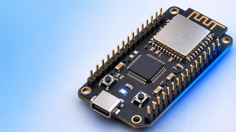
Figure 1: A microcontroller development board with a wireless module and pin headers
This article explains what a development board contains and which features matter. It then compares common ESP32, Arduino, and Raspberry Pi boards and shows how to design and manufacture a custom board to replace them.
What Is a Development Board?
A development board is a complete, working reference circuit for one chip. The power supply, clock, reset, programming path, and pin access are already resolved, so the only remaining open question is your application.
How Development Boards Simplify Hardware Development
A bare microcontroller cannot run on a bench by itself. It needs a regulated supply, decoupling, a clock source, a reset circuit, and a way to load firmware. A development board supplies all of them. Espressif's ESP32-DevKitC, for example, carries an ESP32-WROOM-32E module and a USB-to-UART bridge that runs at up to 3 Mbps. It adds Boot and EN buttons, a power LED, and two 19-pin headers that break out the module's pins.
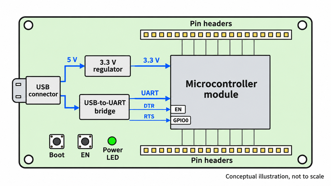
Figure 2: The support circuits a development board adds around its microcontroller
Because the support circuit is known to work, a fault you find is in your code or wiring, not the board. That isolation is the real value, since you can validate a sensor, a protocol, or a control loop in an afternoon, then carry the proven firmware and the same chip into a custom design. The board's published schematic also becomes the starting reference for that design.
Development Board vs. Custom PCB
A development board is built to expose everything, while a custom PCB is built to include only what the product needs. Headers, buttons, LEDs, and spare regulators make a development board flexible on the bench, but they add size, cost, and loose connections that a finished product cannot carry.
| Factor | Development Board | Custom PCB |
|---|---|---|
| Time to first test | Hours | Weeks for design, fabrication, and assembly |
| Size and shape | Fixed by the board | Fitted to the enclosure |
| Hardware on board | Headers, buttons, LEDs, and spare circuits | Only what the product needs |
| Connections | Jumper wires or stacked shields | Soldered traces and locking connectors |
| Cost per unit at volume | Higher, paying for unused parts | Lower, set by your own BOM |
| Wireless certification | Inherited when the board uses a certified module | Inherited with the same module, repeated for a chip-down radio |
Most products move through a middle step: a custom carrier board built around the same certified module. It keeps the proven RF design and firmware and removes everything the product does not need.
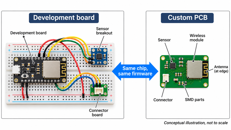
Figure 3: The same circuit on a development board and on a custom PCB
Key Features to Look for in a Development Board
Three sets of features determine if a development board is right for a project: the processor and memory, the I/O it provides, and how it consumes power and firmware. Evaluate each one not just the prototype, but the product you want to produce.
Microcontroller, Memory, and Processing Performance
The chip determines the maximum for all else. Most boards are loaded with a microcontroller, a single chip containing a CPU, flash, and SRAM, and they are run directly from a single firmware image. Single-board computers are equipped with a microprocessor and external RAM and are powered by a complete operating system such as Linux. The first is for deterministic control and low power, while the second is for cameras, displays, and a complete networking stack.
The first limiting factor that generally shows up is memory. The ATmega328P used in an Arduino UNO has 2 KB of SRAM, which is sufficient for reading sensor data and basic control logic, but not for a Wi-Fi stack. The ESP32 has 520 KB of internal SRAM, with external flash added by the modules (4 MB on the WROOM-32E). If possible, select a board with extra space above the prototype firmware, as logging, OTA updates, and security features will expand the image later.
GPIO, Communication Interfaces, and Expansion Options
The number of GPIOs on a board is not equal to the number of usable GPIOs. GPIO6-11 are connected to the SPI flash on ESP32 boards and should not be connected to anything else. The boot mode is reset by the strapping pins GPIO0, GPIO2, GPIO5, GPIO12, and GPIO15; pulling these pins high or low changes the boot mode. The number of pins remaining after these exclusions, NOT the number on the front page of the datasheet.
The interfaces determine which parts you can add without additional chips. Compare the number of UART/SPI/I2C ports, number of ADC channels, their resolution, and the number of PWM outputs with the list of sensors and actuators. Count is not the only thing that matters; so is logic level. The Arduino UNO R3 operates at 5 V; the ESP32 and Raspberry Pi boards operate at 3.3 V I/O, which are not 5 V tolerant, so a level shifter is required if a sensor output is 5 V.
Power Management and Programming Interfaces
The main difference between a development board and a product is the power section. A board is typically powered from a 5V USB source via a regulator, and this doesn't mean much for battery life or supply margin. There are also rules for the supply inputs. The ESP32-DevKitC can only be powered from one port (USB, 5V, 3V3) at a time. Serious damage to the board or source when used in parallel.
There are two types of programming interfaces. The firmware is loaded on the chip by a USB-to-serial bridge via the bootloader. On ESP32 boards, the bridge's DTR and RTS lines are connected to EN and GPIO0, so the flashing tool can reset the chip into download mode without pressing the reset button. A debug port like SWD or JTAG can give breakpoints and register inspection, and will be important when a bug is related to timing. On any board that is made, keep at least one of these paths.
Common Examples of Electronic Development Boards
Electronic development boards fall into two families: microcontroller boards, such as the ESP32, Arduino, and Raspberry Pi, and single-board computers, such as the Raspberry Pi 5. The family decides the software model before any single specification does.
ESP32 Development Boards for IoT Projects
ESP32 development boards are the usual choice when a project needs wireless connectivity. The ESP32 combines a dual-core Xtensa LX6 processor running up to 240 MHz with 2.4 GHz 802.11 b/g/n Wi-Fi and Bluetooth v4.2 BR/EDR and Bluetooth LE on a single chip. It also offers 34 programmable GPIOs and a 12-bit ADC with up to 18 channels. Most boards carry it as a shielded module, so the RF matching and the antenna are already done.
The module choice is the decision that carries into the product. On the DevKitC, the 32E variant uses a WROOM-32E with a PCB antenna, while the VE variant uses a WROVER-E with 8 MB of flash and 8 MB of PSRAM for larger buffers. The 32UE and VIE variants take an external antenna via a connector, which helps with placement inside a metal enclosure. So prototype on the module you intend to ship, and keep the custom board's firmware and RF design the same.
Arduino and Raspberry Pi Development Boards
The Arduino UNO R3 is the reference beginner board, valued for its libraries and shields rather than its speed. A second chip, an ATmega16U2, handles USB, so the main microcontroller stays free for your code. Raspberry Pi makes two kinds of boards. The Pico is a microcontroller board whose programmable I/O (PIO) state machines generate custom digital protocols in hardware. The Pico 2 moves to the RP2350 at 150 MHz with 520 kB of SRAM on the same pinout. The Raspberry Pi 5 is a single-board computer that runs Linux.
| Board | Processor | Memory | I/O | Power Input |
|---|---|---|---|---|
| Arduino UNO R3 | ATmega328P, 8-bit AVR, 16 MHz | 32 kB flash, 2 kB SRAM, 1 kB EEPROM | 14 digital (6 PWM), 6 analog | USB 5 V or VIN 6-20 V |
| Raspberry Pi Pico | RP2040, dual Cortex-M0+, 133 MHz | 264 kB SRAM, 2 MB flash | 26 GPIO, 3 ADC inputs, 8 PIO state machines | USB 5 V or VSYS 2-5 V |
| Raspberry Pi 5 | BCM2712, quad Cortex-A76, 2.4 GHz | 1-16 GB LPDDR4X, microSD storage | 40-pin GPIO header, 3.3 V logic | USB-C, 5 V at 5 A |
Choosing a Development Board for Your Application
Start from the requirement that rules out the most boards. A product that needs Linux, a camera, a display, or heavy networking points to a single-board computer. One that needs Wi-Fi or Bluetooth on a small power budget points to an ESP32 board. Tight timing requirements for custom digital signals favor the Pico and its PIO, while a first project with simple 5 V sensors favors the UNO for its libraries.
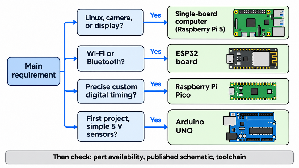
Figure 4: Choosing a development board by what the application needs
Then check the path to production. Prefer a board whose chip or module is sold as a bare part, whose schematic is published, and whose toolchain carries over to a custom board. A part you cannot buy in volume only delays the redesign.
How to Design a Custom Development Board
A custom development board is the reference design trimmed to your product: the same chip, the support circuits it needs, and only the I/O you use. The work splits into choosing the parts, laying them out, and making the board easy to build.
Define Functional Requirements and Select Components
Write the requirements as numbered items before drawing a schematic: supply source and voltage range, peak and sleep current, interfaces and pin count, wireless requirements, operating temperature, and board outline. Each one selects a part. A battery input sets the regulator topology, and the radio sets the module. The interface count then confirms that the chip still has enough free pins after excluding the strapping and flash pins.
Then copy the support circuits from the vendor's checklist, not from memory. For an ESP32, Espressif's schematic checklist calls for a 3.3 V supply rated for at least 500 mA, at least 10 µF at the power input, and 0.1 µF near the supply pins. It also calls for an RC delay on EN, typically 10 kΩ and 1 µF, so the chip leaves reset only after the rails are stable. Keep a USB-to-UART bridge wired for automatic download, or a header for an external one.
Optimize PCB Layout, Routing, and Signal Integrity
The layout for a wireless board starts with the ground plane and the antenna. Espressif recommends a four-layer board with layer 2 as an unbroken ground plane, or, on two layers, a complete ground plane on the bottom under the chip, RF section, and crystal. The module's antenna should either overhang the board edge or sit at the edge, with the board cut away beneath it, because copper near the antenna detunes it. Espressif also recommends at least 15 mm of clearance from the housing in every direction.
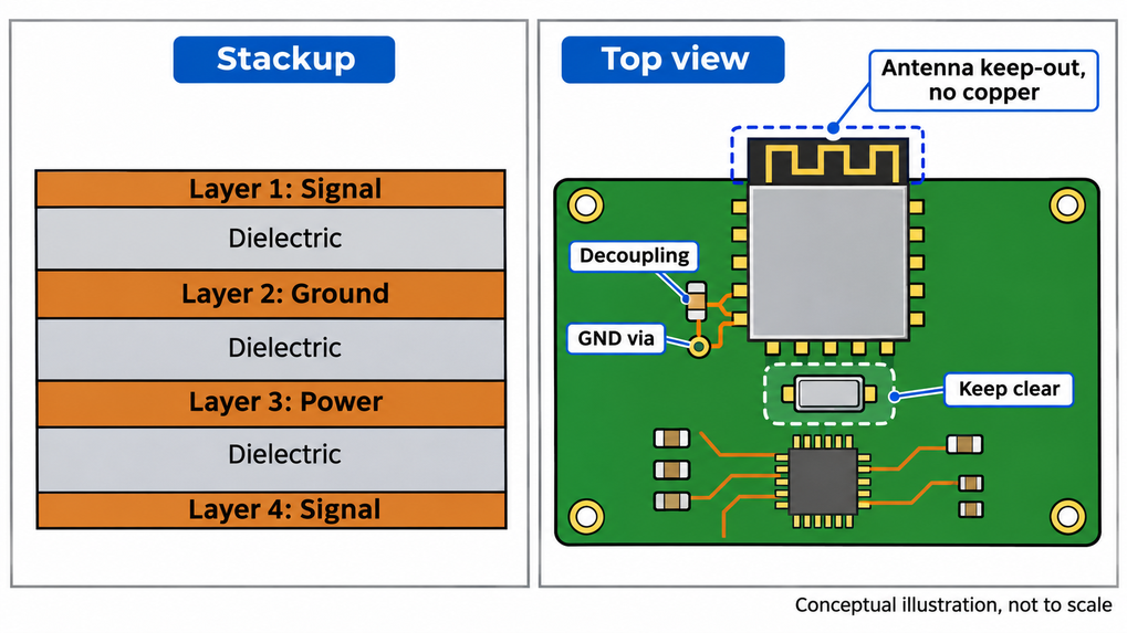
Figure 5: Four-layer stackup and antenna placement for a wireless board
Placement does most of the signal-integrity work on a board like this. Put decoupling capacitors at the supply pins with a ground via beside each, because a short return path keeps supply noise local. Keep the crystal at least 2.7 mm from the clock pin with no traces beneath it. Route any RF trace on the outer layer at 50 Ω without vias. Main 3.3 V traces should be no narrower than 25 mil (0.64 mm). Route the USB data lines together as a differential pair over solid ground.
Design for Manufacturing and Assembly
Design for manufacturing keeps the board inside the fabricator's standard process: Check trace width, spacing, drill size, and annular ring against the fabricator's published limits before routing, not after. Standard rules cost less and fail less often than minimum ones, so use the smallest features only where a module or a fine-pitch part forces them.
Design for assembly keeps the board easy to place, solder, and inspect: Put all surface-mount parts on one side where possible, so the board needs a single reflow pass. Use footprints that match each part's datasheet land pattern, add fiducials for the pick-and-place machine, and leave test points on every supply rail, the UART lines, EN, and GPIO0. Through-hole headers add an extra soldering step, so use them only where a cable or a mating board is required.
From Development Board Design to Reliable PCB Manufacturing
A custom development board is only as reliable as its fabrication, assembly, and first tests. Each of those steps has a decision the designer makes before the order is placed.
Multilayer PCB Fabrication and Stackup Selection
A wireless microcontroller board is usually a four-layer design because a solid ground plane under the chip and RF section is hard to keep intact on two layers when power and signals share the bottom layer. The stackup is also part of the routing. It sets the dielectric height under outer traces, which fixes the width a 50 Ω RF line or a USB pair needs, so draw those traces to the fabricator's real stackup rather than a generic one.
JLCPCB offers 1- to 32-layer board fabrication and standard impedance control for 4-layer or above boards with a tolerance of ±10%. According to the JLCPCB capabilities page, we can achieve a minimum track and spacing of 0.09 mm (3.5 mil) on multilayer boards and a minimum via-hole size of 0.15 mm (0.2 mm preferred). When designing to preferred values rather than minimums, a prototype is maintained on the standard line.
Component Sourcing and PCB Assembly
Sourcing should be a part of design, not after design. Ensure all items listed in the BOM are available at the assembler, have an alternate available if applicable, and are consistent with the drawn footprint before freezing layout. When a module, crystal, or USB-to-UART bridge chosen for the design goes out of stock, it can halt the rebuild of an otherwise proven design.
JLCPCB has over 700,000 in-stock parts in its parts library and offers its assembly service in two types. Economic assembly places parts on one side, down to 0402, for 2 to 50 boards, and Standard assembly places parts on both sides, down to 01005, for 2 to 80,000 boards. Both AOI and X-ray inspection are used for BGA, QFN, and LGA packages, where the joints are located beneath the body and cannot be inspected by a camera. Send your Gerber, BOM, and placement files to receive an instant quote.
Prototype Testing and Production Readiness
Raise the first boards in a particular sequence, with each test depending on the previous ones. Check the assembly, then power the board from a current-limited supply and verify each rail before loading firmware. Then verify the programming path by flashing a minimal image. Then run the same code that was used on the development board on each interface to distinguish hardware problems from firmware problems.
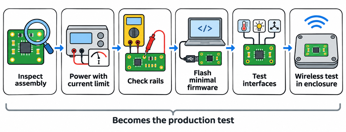
Figure 6: Bring-up order for a first custom development board
Production readiness is a different test: The board must operate in its enclosure, at its temperature extremes, and on each board. Use the board in the final housing to measure the wireless range, as plastic, batteries, and cables in the vicinity of the antenna may detune it. Next, turn the bring-up steps into a short production test, including test points, to ensure all assembled boards are tested the same way.
FAQs about Development Boards
Q: What is a development board used for?
A development board is used to program and test a microcontroller or processor on working hardware before designing a custom circuit. It provides power, a programming interface, and accessible pins, so you can validate firmware, sensors, and interfaces in hours instead of waiting for a custom PCB.
Q: Is Arduino a development board or a microcontroller?
The Arduino UNO is a development board. The microcontroller is the ATmega328P chip. The board adds the USB interface, voltage regulator, headers, and reset circuit, so you can program and connect that chip without building those circuits yourself.
Q: Is a Raspberry Pi a development board?
Yes, but of a different kind. The Raspberry Pi 5 is a single-board computer that runs a full operating system on a microprocessor with gigabytes of RAM. The Raspberry Pi Pico is a microcontroller board that runs a single firmware image, similar to an Arduino or ESP32 board.
Q: Which development board is best for beginners?
The Arduino UNO is the usual first board. Its libraries, examples, and shields cover most beginner sensors and actuators, and its 5 V I/O works directly with many hobby modules. An ESP32 board is a good second step once a project needs Wi-Fi or Bluetooth.
Q: What is the difference between a development board and a development kit?
A development kit is a development board plus the extras needed for a specific application, such as sensors, cables, a debugger, or software. The board is the core, and the kit bundles everything around it so you can start that application without sourcing parts separately.
Conclusion
A development board proves an idea on hardware that already works. That proof carries forward only if the chip, module, and firmware you prototype with are ones you can build into a product. So choose the board by the requirement that rules out the most options, prototype on the module you intend to ship, and copy the vendor's support circuits into a custom board sized to the product.
When your custom board is laid out and checked against your fabricator's limits, order your PCBs and assembly from JLCPCB and bring up the first boards with the test points you designed in.
Popular Articles
• Choosing the Best PCB Color-Enhancing Aesthetics and Functionality
• PCB Silkscreen: All You Need to Know
• The Comprehensive Guide to Circuit Symbols: Key to Understanding Electrical and Electronic Diagrams
• Understanding Electrical Schematics: A Comprehensive Guide
• PCB Board Design: A Step-by-Step Guide for Beginners
Keep Learning
A Beginner's Guide to Basic Electronic Components: Functions, Symbols & Uses
Every circuit, from a simple LED flashlight to a microcontroller board, is built from the same handful of common electronic components. This guide breaks down the ten basic electronic components you will encounter most often: What each component does How it works Key specifications Where engineers use it By the end, you will be able to recognize these electronic circuit components on a schematic, a PCB, or a parts bin, and know exactly why each one is there. These electronic components are the buildin......
Capacitor Voltage Rating Explained with Examples
Capacitors are small components widely used not only for power delivery but also for signal conditioning in electronic circuits. In this article, we focus on the capacitor voltage rating across different types of capacitors. At first glance, capacitors look simple—small cans, discs, or chips on a PCB. However, their markings carry essential design information, including capacitance and voltage rating. These are not arbitrary values but directly affect circuit reliability. Ignoring the voltage rating w......
From Prototype to Product with a Better Development Board
Note Prototype Fast: Development boards integrate power, clock, and programming circuits to validate firmware in hours. Pick the Right Platform: Use ESP32 for Wi-Fi/BLE, Arduino UNO for 5 V sensors, Raspberry Pi Pico for tight I/O timing, and Raspberry Pi 5 for Linux. Scale to Custom PCB: Reuse your prototype's certified module, firmware, and support circuits, but remove unused headers to cut unit cost. Build for Production: Use a 4-layer ground-plane stackup for wireless boards, verify BOM stock earl......
4 Layer vs 6 Layer vs 8 Layer PCB: How to Choose the Right Stackup
Random selection of layers in electronics may lead to serious signal integrity issues. That's why we always design our stackup before designing the PCB. Stackup decides the type of PCB and how it gonna perform under high-frequency conditions. There are a lot of things that directly affect the stackup of the PCB, related to impedance matching, routing density, signal and power integrity, electromagnetic compatibility (EMC), and cost. Knowing the requirements before design and the most critical componen......
Choosing the Best PCB Color-Enhancing Aesthetics and Functionality
Key Takeaways Choosing the best PCB solder mask color involves balancing aesthetics, visibility, and functionality. Green remains the top choice for superior contrast and inspection, while black offers premium appeal, white excels in LED applications, and other colors like purple and red provide unique design options. The ideal color depends on your priorities in inspection ease, thermal performance, and brand image, with minimal impact on electrical performance when using proper silkscreen contrast. ......
Single-Sided PCB Design: Combining Simplicity with Sophistication
Key Takeaways Single-sided PCBs offer a simple, cost-effective solution for many electronic applications. SMT and THT components require different mounting and soldering arrangements. Proper layer orientation, Gerber files, and design rules help ensure manufacturability. Aluminum PCBs require careful attention to insulation, component mounting, and silkscreen placement. A printed circuit board (PCB) provides mechanical support for electronic components and establishes the electrical connections requir......