
How Impedance Controlled Routing Delivers Reliable High-Speed PCB Performance
14 min
- Why Impedance Controlled Routing Is Essential for High-Speed Designs
- Key Techniques for Effective Impedance Controlled Routing
- Material and Stackup Choices That Support Impedance Control
- Manufacturing Precision Required for Accurate Impedance
- JLCPCB's Expertise in Impedance Controlled Routing
- FAQ about Impedance Controlled Routing
Key Takeaways
Impedance Controlled Routing is essential for reliable high-speed PCB performance above 1 Gbps, eliminating reflections, ringing, and bit errors by precisely targeting interface-specific impedances (USB 90 Ω, PCIe 85 Ω, DDR4 40/80 Ω, HDMI 100 Ω) through field-solver calculations, symmetrical stackups with continuous reference planes, stable low-loss dielectrics, and strict single-ended/differential routing rules. Manufacturing precision in etching, copper profile, and lamination, verified by TDR testing to ±10% tolerance, ensures consistent results from prototype to volume production at JLCPCB.
Have you ever created a PCB that passed all your design rule checks with flying colors only to find out that your high-speed signals were riddled with reflections, ringing, and inexplicable data errors when the board returned after fabrication? Probably otherwise, you have found out the results of uncontrolled impedance. The art of routing with impedance control is what lies between a schematic model that simulates and a physical board that works. In its absence, all of your high-speed traces on your board are gambles. When the data rates rise above the 1 Gbps threshold, and the signal edge rates fall below a nanosecond, copper traces on your PCB cease to act like wires and begin to act like transmission lines. At this stage, the characteristic impedance of individual traces is equally significant as ensuring that the netlist connectivity is correct.
Even a 10-15 percent mismatch between the trace impedance and the driver or receiver impedance can result in a strong enough reflection to close an eye diagram and introduce bit errors. This article will discuss why impedance-controlled routing is a must in modern high-speed design, and will proceed to walk through the most important techniques of calculating and targeting impedance values, material and stackup selections that allow consistent impedance, and finally look at the manufacturing accuracy that is necessary to hold impedance within specification. We will also discuss how the fabrication capabilities of JLCPCB can help achieve accurate impedance control between prototypes and volume production.
Why Impedance Controlled Routing Is Essential for High-Speed Designs
Understanding Impedance and Its Impact on Signal Integrity
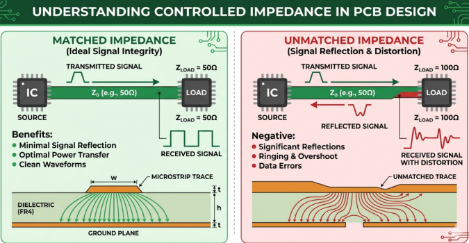
Each trace on a PCB is a copper trace and has a characteristic impedance based on its physical geometry and the characteristics of the dielectric surrounding it. In the case of a microstrip trace on the outer trace, the trace width, copper thickness, height above the reference ground plane, and the dielectric constant (Dk) of the laminate are all factors determining the impedance. In the case of a stripline trace surrounded by two reference planes, the same considerations are applicable, except that the geometry is symmetrical.
This characteristic impedance is perceived as a continuous property of the transmission line when a high-speed signal is propagating along a trace. When the impedance is the same throughout the length, and the impedance is properly terminated at both ends, the signal flows cleanly between the driver and receiver. When the impedance varies at any point along the path, a fraction of the signal energy is reflected back in the direction of the source. The size of this reflection is determined by the reflection coefficient, which is determined by the difference between the two impedance values divided by the sum of the two impedance values.
The target values of the impedance of common high-speed interfaces are well defined. USB 2.0 and USB 3.0 need 90 ohm differentials. PCIe defines 85 ohm differential impedance. DDR4 memory buses have 40-ohm single-ended traces and 80 ohm differential pairs. HDMI needs 100 ohms of differing impedance. Failure to meet these targets within a more than allowed tolerance, usually within the range of plus or minus 10 percent, causes signal integrity failures directly.
Common Problems When Impedance Is Not Controlled
In high-speed designs, the symptoms are manifested very soon when impedance is not controlled. Signal reflection is the nearest issue. Each impedance discontinuity of a trace, whether due to a change in width, a via transition, or a connector interface, is a reflection that reflects back to the source. These considerations overprint the original signal and cause overshoot, undershoot, and ringing at each transition edge.
The second significant issue is crosstalk amplification. With the random variation of trace impedances across the board, the interaction between neighboring traces becomes random. Both near-end crosstalk (NEXT) and far-end crosstalk (FEXT) are enhanced when the traces are not routed at controlled impedances on defined reference planes. The rule of 3W spacing is beneficial, but it cannot offset the essentially uncontrolled trace geometry.
Key Techniques for Effective Impedance Controlled Routing
Calculating and Setting Target Impedance Values
The principles of controlled impedance routing are to know your target values in advance of routing. These values are obtained in two ways: the interface specification and the impedance calculation of your stackup geometry. In the case of single-ended microstrip traces, the characteristic impedance can be estimated by the well-known formula:
Z0 = (87 / sqrt(Er + 1.41)) x ln(5.98 x H / (0.8 x W + T))
Where Er is the dielectric constant of the substrate, H is the height of the dielectric between the trace and the reference plane, W is the trace width, and T is the copper thickness. This formula is reasonable to make first estimates; however, a field solver should always be used in production designs to get accurate results. Such tools as the Polar Instruments Si9000 or the built-in integrated impedance calculators in Altium Designer and KiCad are accurate at the field-solver level.
Routing Strategies for Single-Ended and Differential Pairs
After you have decided on your target impedance values and have calculated your trace widths, the routing strategy will decide whether to keep those values the same throughout the signal path.
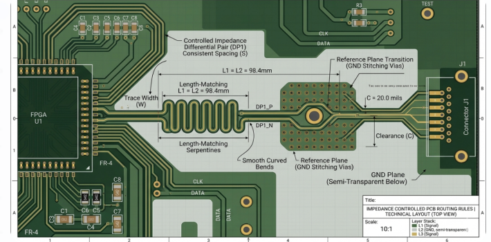
In single-ended controlled impedance traces, the following are some of the important routing guides:
1.Have a constant reference plane next to the signal layer. Any discontinuity in the reference plane of a controlled impedance trace kills the local impedance and forms an enormous discontinuity.
2.Make trace widths the same throughout the route. You should not neck down traces to squeeze through cracks unless absolutely necessary, and when you do, the necked-down section should be as short as possible.
3.Minimize through inter-layer transitions. Capacitive discontinuity is created by each via, and locally decreases impedance. Where layer changes are inevitable, stitching should be used to offer a close alternate path to the reference plane current.
4.Have sufficient clearance between neighboring traces and copper pours. Close conductors alter the effective impedance of a trace, capacitively.
| Interface | Impedance Type | Target Value (ohm) | Typical Tolerance | Trace Geometry |
|---|---|---|---|---|
| USB 2.0 | Differential | 90 | +/- 10% | Microstrip or stripline |
| USB 3.0 / 3.1 | Differential | 90 | +/- 10% | Stripline preferred |
| PCIe Gen3/4/5 | Differential | 85 | +/- 10% | Stripline preferred |
| DDR4 | Single-ended | 40 | +/- 10% | Microstrip |
| DDR4 | Differential (clock) | 80 | +/- 10% | Microstrip |
| HDMI 2.0 | Differential | 100 | +/- 10% | Microstrip or stripline |
| Ethernet 1000BASE-T | Differential | 100 | +/- 10% | Microstrip or stripline |
| LVDS | Differential | 100 | +/- 10% | Stripline preferred |
| 50 ohm RF | Single-ended | 50 | +/- 5% to 10% | Microstrip or CPWG |
Material and Stackup Choices That Support Impedance Control
Selecting Laminates with Stable Dielectric Properties
One of the first variables in all impedance calculations is the dielectric constant of your PCB laminate. Unless that number is steady and well defined, the trace widths that you compute will not give you the desired impedance on the board you are making. Depending on the resin content, the weave style of the glass, and the frequency of measurement, standard FR4 has a dielectric constant (Dk) that varies between about 4.2 and 4.7. The first difficulty is that variation. A 0.3 difference in Dk can change your impedance by 3-5 percent, directly consuming your tolerance budget.
The dielectric loss tangent (Df) also becomes significant at designs greater than 5 GHz. DF of the standard FR4 is about 0.017 to 0.025, and this leads to high signal attenuation at high frequencies. Laminates with much lower loss, such as the Isola I-Speed (Dk 3.63, Df 0.0085) or the Panasonic Megtron 6 (Dk 3.4, Df 0.002), are dramatically lower loss, but also differ in the values of Dk, which modifies all your impedance calculations. When changing materials, you have to recalculate all the trace widths.
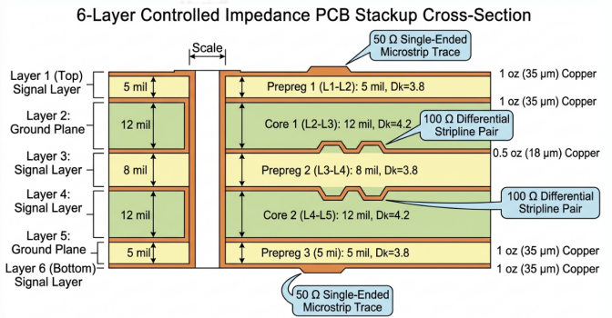
Layer Stackup Optimization for Consistent Impedance
The structural basis that defines the impedance of each trace on the board is the layer stackup. The stackup is not an option in controlled impedance designs. It is the most crucial design choice that you will make.
An impedance control stackup is designed to adhere to a few principles:
- Each signal layer must have a directly adjacent, continuous reference plane. In the case of a 4-layer board, the standard signal-ground-power-signal configuration offers a ground plane reference on the upper layer and a power plane reference on the bottom layer.
- Symmetrical stackups are preferred. A symmetrical stackup also balances the copper distribution between the board thickness and minimizes warpage in the lamination process, and eliminates dielectric-thickness variations after pressing.
| Layer Count | Recommended Stackup | Signal Layers | Reference Planes | Impedance Control Quality |
|---|---|---|---|---|
| 2-layer | Signal / Signal | 2 (outer) | None (ground pour) | Basic, limited control |
| 4-layer | Sig / GND / PWR / Sig | 2 (outer) | 2 (inner) | Good for most designs |
| 6-layer | Sig / GND / Sig / Sig / PWR / Sig | 4 | 2 | Very good, inner stripline possible |
| 8-layer | Sig / GND / Sig / GND / PWR / Sig / GND / Sig | 4 | 4 | Excellent, full stripline routing |
Manufacturing Precision Required for Accurate Impedance
Etching Tolerance, Copper Profile, and Registration Control
The half of the equation is designed to control impedance. The fabrication process should be able to reproduce your target trace geometry with accuracy good enough to keep the target impedance within tolerance. A number of manufacturing parameters have a direct influence on the impedance that is achieved on the completed board.
The most important one is etching tolerance. In the chemical etching process, the copper is not only etched vertically, but also horizontally in a process known as undercut. This cross-section is trapezoidal, such that the completed trace is thinner at the top than at the bottom. In normal etching operations, the undercut may be 0.5 to 1.5 mils on both sides of the effective trace. A trace etched 6 mils can be effective at the top surface with a width of 4 to 5 mils. Fabricators offset this by pre-widening the artwork, although the precision of this pre-widening has a direct impact on the ultimate impedance.
Copper profile: The surface of the copper foil bonded to the dielectric is rough and is known as the copper profile. Common electrodeposited (ED) copper comes in a roughness profile of 5 to 10 micrometers (standard profile) to 1 to 3 micrometers (very low profile, VLP). This ruggedness adds to the effective conductor loss at high frequencies and has a subtle impact on the impedance as it alters the effective boundary between copper and dielectric. In designs above 10 GHz, it is important to specify reverse-treated foil (RTF) or hyper-very-low-profile (HVLP) copper.
Registration control is a process that makes sure that all layers within a multilayer board are aligned perfectly with the other layers. When the signal layer moves with respect to its reference plane during lamination, the effective dielectric height of one side of the trace changes, resulting in an impedance asymmetry. Recent fabrication devices have a registration accuracy of between 2 and 3 mils plus or minus, but this should be checked by cross-sectional analysis on production coupons.
Lamination control of dielectric thickness is also important. The prepreg layers creep and squeeze during the hot-press lamination cycle, and the ultimate dielectric thickness is determined by the lamination pressure, temperature field, and copper density on the layers above and below. Regions having large copper pours squeeze the prepreg less than those with small copper pours, resulting in localized dielectric thickness variations. This effect can be reduced with the aid of copper balancing techniques.
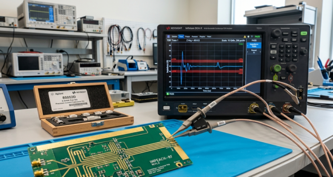
Testing and Verification Methods in Production
Controlled impedance boards must be tested to verify that the manufactured impedance matches the design specification. The industry standard tool for this measurement is the Time Domain Reflectometer (TDR). A TDR works by sending a fast-rise-time pulse down a test coupon trace and measuring the reflected signal. The reflection profile along the trace length reveals the impedance at every point. Any discontinuities, variations, or deviations from the target impedance are visible in the TDR plot.
The test coupons are included in the panel borders alongside the production boards, manufactured using the same processes, and represent the impedance performance of the actual product. The standard test protocol follows IPC-TM-650 2.5.5.7, which specifies the TDR measurement method for characteristic impedance of transmission lines on printed boards. Each impedance-controlled layer is tested independently, and the results are documented on an impedance test report that ships with the order.
JLCPCB's Expertise in Impedance Controlled Routing
Advanced Fabrication Processes for Precise Impedance Matching
JLCPCB has invested heavily in the fabrication precision needed to deliver consistent impedance-controlled boards. The manufacturing process for impedance-controlled orders includes pre-production impedance modeling using field-solver calculations calibrated to the actual material properties and process parameters of the production line. This means the etch compensation, dielectric thickness targets, and trace width adjustments are tuned specifically for the material and stackup you specify.
Every impedance-controlled order includes TDR testing per IPC-TM-650 2.5.5.7 on dedicated test coupons. The impedance test report is provided with the shipment, giving you documented verification that the manufactured boards meet the specified impedance targets within the tolerance band. This level of process control is available on standard production orders, not just premium or expedited jobs.
Reliable Results from Prototypes to Volume Production
Consistency between prototype and production is a critical concern for impedance-controlled designs. A board that measures 50 ohm on the prototype run must still measure 50 ohm when you scale to 10,000 units. JLCPCB achieves this consistency through standardized material sourcing, documented process recipes for each material and stackup combination, and statistical process control on critical parameters like etch factor and dielectric thickness.
For prototype quantities, JLCPCB offers impedance-controlled boards with production times starting at 1 to 2 days for standard stackups, making it feasible to iterate quickly on your impedance-controlled designs without long lead times. The pricing starts from $2 for standard PCBs, and the impedance control option adds a modest premium that is well justified by the TDR testing and tighter process controls included.
FAQ about Impedance Controlled Routing
Q: What is impedance-controlled routing, and when do I need it?
Impedance-controlled routing is the practice of designing and manufacturing PCB traces to achieve a specific characteristic impedance, verified through TDR testing during fabrication. You need it whenever your design includes high-speed interfaces like USB 3.0, PCIe, DDR4, HDMI, Ethernet, or any signal with edge rates faster than approximately 1 nanosecond.
Q: What is the typical impedance tolerance for controlled impedance PCBs?
The standard manufacturing tolerance for controlled impedance is plus or minus 10 percent. This means a 50 ohm target will be accepted if the measured impedance falls between 45 and 55 ohm. For differential pairs at 100 ohm, the acceptable range is 90 to 110 ohm.
Q: How does the stackup affect controlled impedance?
The stackup defines the dielectric height between each signal layer and its reference plane, which is one of the primary variables in the impedance equation. Changing the prepreg type, adding or removing copper layers, or rearranging the layer order all change the dielectric height and therefore the impedance.
Q: Can I achieve controlled impedance on a 2-layer PCB?
Yes, but with limitations. On a 2-layer board, controlled impedance is achieved using microstrip geometry with a ground copper pour on the opposite layer. The challenge is that the ground pour may have gaps and voids that disrupt the reference plane continuity, making impedance less predictable than on multilayer boards with dedicated solid ground planes.
Popular Articles
Keep Learning
Optimizing Power Nets for Stable and Efficient High-Performance PCBs
Key Takeaways Power Nets as Systems: It is a complete copper network of planes, pours, traces, and vias built to deliver clean, stable voltage. Control IR Drop: Copper resistance causes voltage drop. Use wider traces, solid pours, or heavier copper (2 oz+) to stay within voltage tolerances. Minimize Loop Area: Place decoupling capacitors close to power pins with short, wide traces to handle fast transient currents. Scale Your Vias: A single 0.3mm via carries only 1 to 2A. High-current paths require pa......
Achieving Stable Power Delivery : Mastering PDN Impedance in High-Performance PCBs
Key Takeaways PDN impedance directly determines voltage stability under load. Keep it low and flat. Calculate your target: Z_target = (V_dd × Ripple%) / I_transient — typically single-digit milliohms. Prioritize close power-ground planes, short via connections, and strategic decoupling placement. Avoid anti-resonance peaks; a smooth curve matters more than raw capacitance. Precise manufacturing (copper thickness, dielectric control) is essential to match simulation results. There's no point in using a......
Phase Matching in High-Speed PCB Design: Achieving Signal Integrity with Precision Manufacturing
Key Takeaways Phase matching controls electrical trace length in high-speed PCBs to maintain precise signal timing and phase relationships. Even 10–15 ps skew (roughly 1–2 mm difference) at 10 Gbps can collapse eye diagrams, raise bit error rates, and cause system failures. Dynamic phase matching maintains alignment throughout the entire signal path, accounting for bends, vias, and layer transitions. USB 3.x SuperSpeed interfaces commonly target intra-pair skew below 5 mils (0.13 mm) to maintain relia......
Mastering Split Planes for Cleaner Power Delivery and Better Signal Integrity
Key Takeaways Split power planes when needed for multiple voltage domains or analog/digital isolation, but never split ground planes — always keep ground continuous for clean return paths. Avoid routing high-speed signals across splits; if unavoidable, use stitching capacitors (0.1 µF) and ensure differential pairs cross together. Place split power planes next to a solid ground layer, maintain ~10 mil moat width, and use proper decoupling near IC pins. Good split plane design significantly reduces noi......
Building Stable Power Delivery for High-Performance PCBs with Power Integrity Analysis
Key Takeaways Power integrity analysis is essential for building stable power delivery in high-performance PCBs. By maintaining low PDN impedance, optimizing decoupling capacitors, and designing robust power/ground planes with minimal voltage droop and inductance, engineers can prevent common failures such as voltage droop, ground bounce, and power-induced jitter. Combining thorough PI simulation with smart layout practices and professional manufacturing ensures reliable performance from prototype to ......
How Impedance Controlled Routing Delivers Reliable High-Speed PCB Performance
Key Takeaways Impedance Controlled Routing is essential for reliable high-speed PCB performance above 1 Gbps, eliminating reflections, ringing, and bit errors by precisely targeting interface-specific impedances (USB 90 Ω, PCIe 85 Ω, DDR4 40/80 Ω, HDMI 100 Ω) through field-solver calculations, symmetrical stackups with continuous reference planes, stable low-loss dielectrics, and strict single-ended/differential routing rules. Manufacturing precision in etching, copper profile, and lamination, verifie......