Choosing the Right PCB Solder Mask Material for Reliable PCBs
15 min
- What Is PCB Solder Mask?
- Understanding Solder Mask Material Composition
- Common Types of Solder Mask Materials
- How Solder Mask Material Affects PCB Performance
- Selecting Solder Mask Materials for PCB Manufacturing
- How Professional PCB Manufacturing Controls Solder Mask Quality
- FAQ About PCB Solder Mask Material
- Conclusion
Key Takeaways
- Dual-Curing: UV defines openings; heat cures epoxy for durability.
- LPI vs. Coverlay: LPI for rigid boards; coverlay for flexible circuits.
- Color & Pitch: Green allows tighter dams (0.10 mm) than black/white (0.13 mm).
- Protection: Prevents solder bridges and seals copper from moisture.
- Cure Quality: Proper baking prevents mask peeling during plating and reflow.
PCB solder mask material is a cured polymer film usually 10 to 30 µm (0.4 to 1.2 mil) thick. During reflow, it is the only barrier between neighboring pads full of molten solder. Most designers pick it as a color on the order form, but its chemistry matters far more. A solder mask is really two chemistries sharing one layer. The first reacts to ultraviolet light, allowing the factory to photograph your pad openings onto film. The second hardens only in an oven, and it allows the film to withstand solder heat, plating baths, and humidity.
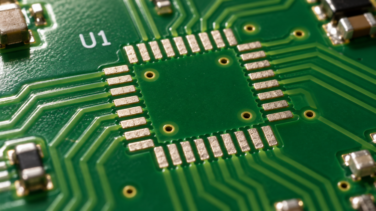
Figure 1: Green LPI solder mask around a fine-pitch footprint
Every mask balances those two jobs, so the ink that images the finest dams is not always the toughest. This guide explains what goes into the material and how LPI compares with dry film and coverlay. It also shows how each property appears in service so that you can match a mask to your application.
What Is PCB Solder Mask?
Solder mask is the permanent coating left on a finished board, unlike the temporary resists stripped off after etching. It works hardest during soldering, but it protects the copper for the board's whole life.
The Role of Solder Mask on a PCB
Solder mask, also called solder resist, is a thin polymer layer over the outer copper. It covers everything except the pads you intend to solder. Molten solder wets bare copper but not cured polymer, so the mask confines each joint to its own pad.
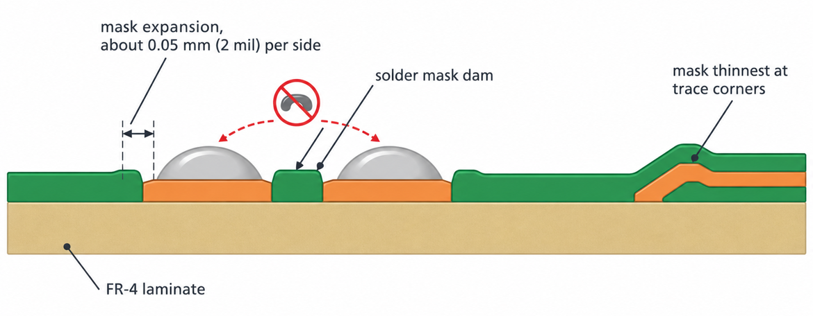
Figure 2: Cross-section of solder mask, pad openings, and a mask dam
On fine-pitch parts, that confinement depends on a narrow strip of mask between pads, called a dam. Each opening is drawn about 0.05 mm (2 mil) larger than its pad per side, so slight artwork misalignment still leaves the pad clear. Oversized openings erase the dam, which is why solder mask expansion rules matter most on tight pitches.
How Solder Mask Supports PCB Protection and Reliability
Bare copper oxidizes in air, and a humid board with flux residue can grow conductive paths between traces. Under bias, those paths can become metal filaments that short two nets, a failure called electrochemical migration. Solder mask seals the copper away from moisture and contamination, so only the exposed pads need a surface finish.
The mask also takes the scratch when a tool slips during rework, so the trace underneath keeps its full width. Fewer bridged joints and damaged traces mean fewer reworked boards, and each rework is an unneeded heat cycle.
Understanding Solder Mask Material Composition
A solder mask is a formulated ink rather than a single polymer. Each ingredient adds one property the film would otherwise lack, so the recipe explains how a mask behaves.
Key Components of Solder Mask Materials
Most liquid masks ship as two parts, a resin base and a hardener, because the parts start reacting once mixed. Together, they carry five ingredient groups:
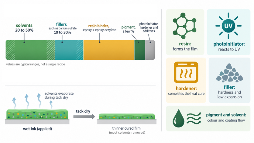
Figure 3: Solder mask material composition by ingredient group
- Resin binder, usually epoxy blended with epoxy acrylate for UV reactivity.
- A photoinitiator that absorbs UV and reacts when light is applied.
- Thermal hardener, such as dicyandiamide or melamine, which completes the epoxy cure.
- Fillers, mostly barium sulfate, make up roughly 10-30% of the ingredients by weight.
- Pigments, solvents, and additives, which set color, viscosity, and leveling.
The first three form one curing system that works in two stages. UV light activates the photoinitiator, which crosslinks the acrylate only in exposed areas. Those areas stop dissolving in the developer, so they become the mask. The epoxy stays partly reacted until the final bake, when the hardener completes the network.
Properties That Matter in PCB Manufacturing
A mask must survive the factory before it protects anything, so fabricators judge an ink first by its process windows. The values below are typical for LPI inks such as Taiyo PSR-4000.
| Process Property | Typical Window | What Goes Wrong Outside It |
|---|---|---|
| Tack dry | About 80°C for 15 to 30 minutes | Too short leaves a sticky film; too long partly cures it |
| Exposure energy (UV lamp) | 250 mJ/cm² or more | Too low washes dams away; too high closes openings |
| Developer | 1% sodium carbonate at 29 to 35°C | Too weak leaves residue on pads; too strong undercuts dams |
| Final cure | About 150°C for 60 minutes | Undercure invites chemical attack; overcure embrittles the film |
| Minimum dam (JLCPCB, 1 oz copper) | 0.10 mm (4 mil) green, red, yellow, blue, or purple; 0.13 mm (5 mil) black or white | Narrower dams break off, and the pads bridge |
Common Types of Solder Mask Materials
Solder masks are classified by how the material is applied to the board and how the openings are formed. Five types cover almost every board built today, but only one is a default:
- Liquid photoimageable (LPI), a liquid ink coated over the panel and imaged with UV.
- Dry film photoimageable, a Dry-film photoimageable sheet laminated under vacuum.
- Screen-printed epoxy, a heat-cured ink printed through a patterned mesh.
- UV-curable inkjet, an ink jetted only where a mask is wanted.
- Polyimide covea rlay, an adhesive-backed film used on flexible circuits.
Liquid Photoimageable Solder Mask
LPI is applied to the entire panel as a liquid via screen printing, spraying, or curtain coating. Because the liquid flows between traces before it dries, it seals the base of every trace. Exposure through artwork, or by laser direct imaging, then fixes the openings photographically.
LPI holds dams down to about 0.1 mm (4 mil) at low cost, making it the default for rigid boards. Its weakness is thickness control because the liquid drains off the top corners of each trace as it levels. Trace edges therefore carry far less mask than the laminate beside them, so abrasion and breakdown usually start there.
Dry Film and Other Solder Mask Materials
Dry film solder mask arrives as a solid photosensitive sheet, typically 50 to 100 µm (2 to 4 mil) thick. It is laminated under vacuum, and its even thickness tends to clean over via holes. However, a solid sheet cannot flow into the gap beside a tall trace so that air can be trapped there.
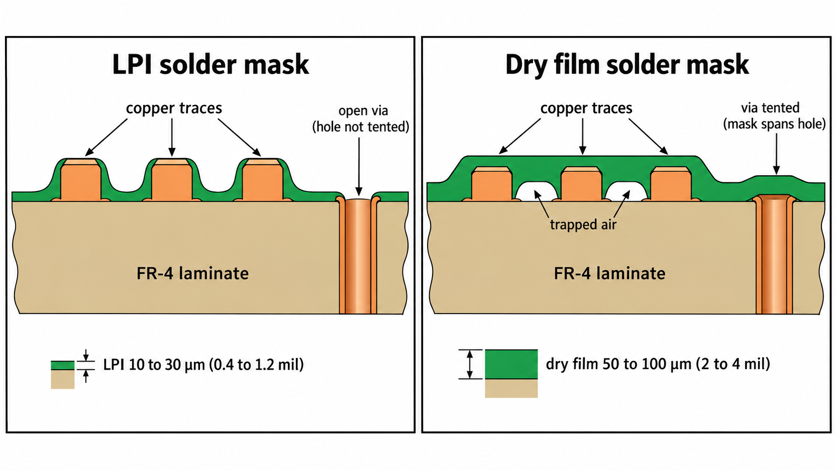
Figure 4: How LPI and dry film conform to copper traces
Screen-printed epoxy is the cheapest option because the mesh itself defines the openings, but a mesh cannot hold fine particles. Inkjet masks such as the Taiyo IJSR-4000 are jetted only where they belong, so no artwork is needed. Cured LPI cracks when a flex circuit bends repeatedly, so polyimide coverlay replaces it, as explained by how flex coverlay protects flexible PCBs.
| Mask Type | How Openings Are Formed | Main Limitation | Best Fit for Your Board |
|---|---|---|---|
| LPI | UV exposure or LDI | Thin at trace corners | Nearly every rigid board, including fine pitch |
| Dry film | UV exposure of a laminated sheet | Air traps beside tall traces | Flat boards needing tented vias |
| Screen-printed epoxy | Pattern in the printing mesh | Coarse features only | Low-cost, wide-pitch boards |
| UV inkjet | Printed from design data | Few fabricators offer it | Prototypes and short runs |
| Polyimide coverlay | Cut or drilled before lamination | Extra lamination step | Flex and rigid-flex bend areas |
How Solder Mask Material Affects PCB Performance
Once cured, the mask stays on the board for life. Its chemistry, therefore, sets the limits on heat, chemicals, voltage, and adhesion.
Thermal and Chemical Resistance
A cured epoxy mask is a thermoset, so it does not melt when solder does. It still has to survive every heat cycle, including lead-free reflow peaks of about 245-250°C on each side. A fully cured film passes through unchanged, whereas an undercured one softens, blisters at pad edges, or discolors.
The chemical attack arrives even earlier because the mask goes on before the surface finish. ENIG plating holds the board in a nickel bath at near-85 °C. An undercured mask leaches into the bath, which then creeps under it and lifts it at the pad edges. Fabs therefore confirm the cure with the solvent resistance test in IPC-TM-650 2.3.42.
Electrical Insulation and Surface Protection
IPC-SM-840E is the qualification standard for permanent solder masks. It requires at least 500 V DC of dielectric strength per 25 µm (1 mil) of film. That rating assumes nominal thickness, but a trace corner carries far less. So on high-voltage nets, copper spacing provides the isolation, and the mask only adds margin.
The mask is also a dielectric resting on every outer-layer trace. Rogers Corporation quotes a typical LPI mask with a dissipation factor of about 0.025 at 1 GHz, compared with 0.0037 at 10 GHz for its RO4350B laminate. That loss is negligible on most digital boards, but on an RF feed, it adds loss and lowers microstrip impedance, so include the mask in the impedance model.
Adhesion and Manufacturing Compatibility
Mask adhesion is mostly decided before any ink touches the board. Fabs brush or micro-etch the copper first, because ink grips a fresh, roughened surface far better than oxidized copper. The tape test in IPC-TM-650 2.4.28.1 then checks the result: tape is pulled off within one minute, and the mask it lifts decides pass or fail.
Legend ink for the PCB silkscreen is printed straight onto the cured mask. After assembly, a conformal coating has to wet and grip it as well. Surface texture matters too, since glossier masks are associated with more solder balls and bridges, so many assemblers prefer matte finishes on fine-pitch boards.
Selecting Solder Mask Materials for PCB Manufacturing
Selection starts from where the board operates and what it carries, then works back to a material and a color. Most boards end up on green LPI, so the useful skill is spotting the ones that should not.
Matching Materials to PCB Applications
IPC-SM-840E qualifies inks to two classes, so the application decides which one you need. Class T covers telecom, computing, and instrumentation. Class H covers equipment where downtime cannot be tolerated, such as life-support and military systems. It also decides the color and whether some traces should carry a mask at all.
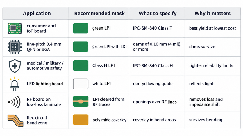
Figure 5: Matching applications to mask material, class, and color
| Application | Recommended Mask | What to Specify | What This Means for Your Board |
|---|---|---|---|
| Consumer and IoT | Green LPI | IPC-SM-840 Class T | Best yield at the lowest cost |
| Fine pitch, 0.4 mm (16 mil) QFN or BGA | Green LPI, LDI imaged | Dams of 0.10 mm (4 mil) or more | Green images are sharpest, so dams survive |
| Medical, military, automotive safety | Class H LPI | IPC-SM-840 Class H | Tested to tighter reliability limits |
| LED lighting | White LPI | Non-yellowing grade | Reflects light, but standard white yellows |
| RF on low-loss laminate | LPI cleared from RF traces | Openings over RF lines | Removes the mask's loss and impedance shift |
| Flex bend zones | Polyimide coverlay | Coverlay in all bend areas | Survives bending that cracks the LPI |
Balancing Reliability, Manufacturability, and Cost
A mask's real cost is set more by yield and process steps than by the ink price. Green LPI is the cheapest because it images best and fails least. A pigmented color narrows the imaging window, and a coverlay adds a lamination step. Those limits feed into your PCB design rules. Three mistakes recur even among experienced designers:
- Specifying a black mask under a 0.4 mm (16 mil) pitch QFN costs you the dam. A 0.2 mm (8 mil) gap, minus 0.05 mm (2 mil) expansion per side, leaves 0.10 mm (4 mil), which is below the 0.13 mm (5 mil) black minimum, so use green.
- Setting mask expansion to zero everywhere puts the mask on the pads whenever registration drifts, starving the joints. Keep 0.05 mm (2 mil) per side unless your fab confirms LDI openings.
- Asking for Class H ink on a consumer product narrows the fab's ink choice for no field benefit. Many mainstream inks, such as Taiyo PSR-4000 HFX, already meet both classes, so specify Class T there.
Green LPI is the cheapest mask because it yields the best, not because its ink is cheap. Change the material only when the application gives you a reason.
How Professional PCB Manufacturing Controls Solder Mask Quality
A mask's datasheet values reach the board only when the ink, coating, and cure all stay within their windows. So fabricators such as JLCPCB control all three, through material checks, a fixed sequence, and final inspection.
Material Selection and Process Control
Production inks are chosen from those qualified to IPC-SM-840E. They are also UL recognized with the laminate they coat, because flammability is rated on the finished construction. Two-part inks start reacting once mixed, so they are prepared in measured batches and used within their pot life.
Exposure is checked routinely with a Stouffer 21-step tablet, a strip of graded film exposed beside the panel. The number of steps left solid after developing shows the energy the mask received. Developer strength and temperature are also logged because a drifting bath undercuts dams before anyone notices a defect.
Solder Mask Application and Curing
Every LPI line runs the same six steps, and each one relies on the step before it:
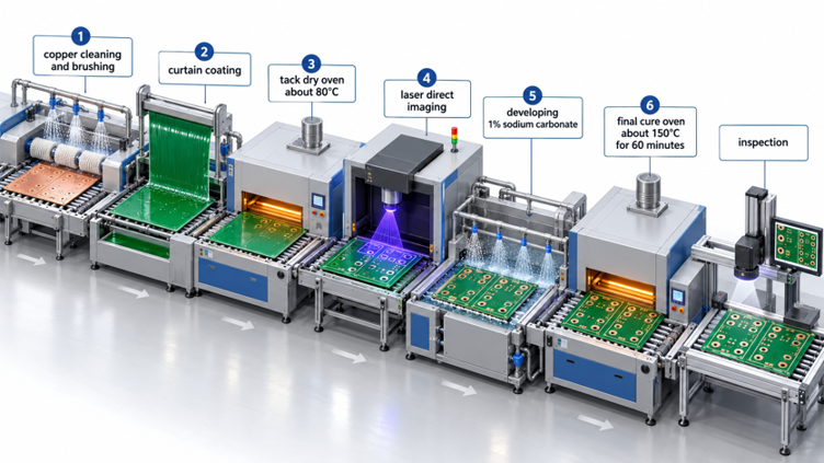
Figure 6: The LPI solder mask process from cleaning to final cure
- Clean and roughen the copper by brushing or micro-etching.
- Coat the panel by screen, spray, or curtain coating.
- Tack-dry at about 80°C to remove the solvent without curing the epoxy.
- Exposure through artwork, or by laser direct imaging without film.
- Develop in 1% sodium carbonate to clear the pad openings.
- Final cure at about 150°C for 60 minutes to complete the epoxy network.
Silkscreen and the surface finish come after step six, so a weak cure rarely shows at the mask station. It appears later, in the ENIG line or in reflow, which is why the cure is controlled as tightly as the exposure.
Inspection and Quality Control
Inspection checks the mask for coverage, registration, and adhesion. Optical inspection compares each panel against the design data and flags mask-on pads, skips, and shifted openings. Acceptance limits come from IPC-A-600, so a defect is judged against a published class rather than an operator's opinion.
JLCPCB offers LPI for rigid boards in seven colors and publishes a minimum design for each, so you can check the footprints before ordering. The JLCPCB quote page prices color, copper weight, and surface finish together, so these trade-offs show up before anything is built.
FAQ About PCB Solder Mask Material
Q: What is the difference between solder mask and conformal coating?
Solder mask is applied by the fabricator before assembly, leaving the pads open for soldering. Conformal coating goes over the finished assembly, so it also covers the components and joints. A board can carry both, since each protects a different stage.
Q: Why did the fabricator remove the solder mask between my IC pads?
Your dam was narrower than the fab's minimum, about 0.1 mm (4 mil) for green mask, so it would have broken off during developing. The fab instead opens one window across the pad row, called a gang relief. Most fine-pitch parts still solder well, but the risk of bridging increases.
Q: Can I repair scratched or missing solder mask myself?
Yes, small areas can be repaired with UV-curable mask sold in syringes or pens. Clean the copper, apply a thin layer, and cure it under a UV lamp. The repair restores corrosion protection, but it will not match factory thickness or resolution.
Q: Is there a halogen-free PCB solder mask material?
Yes, ink makers offer halogen-free grades, such as the Taiyo PSR-4000 HFX series. Check that your fabricator stocks one before you specify it, because standard quotes assume a conventional ink.
Q: Does solder mask color change how my circuit performs electrically?
For almost every design, the effect is negligible because dielectric behavior comes mainly from the resin and filler. Color matters more in manufacturing, where black and white need wider dams, and in inspection, where dark masks hide defects.
Conclusion
Choosing the right PCB solder mask involves more than selecting a color. The material's chemical properties determine how effectively it protects copper traces, withstands soldering temperatures, and provides electrical insulation. Most liquid photoimageable (LPI) solder masks undergo two curing stages. First, ultraviolet (UV) exposure defines precise openings around solder pads and components.
For most PCB designs, green LPI solder mask remains a reliable and cost-effective choice. However, different colors and materials may be better suited to specific requirements, particularly for densely populated boards with fine-pitch components. When planning your next PCB, JLCPCB's instant quote tool can help you explore available solder mask options and select one that meets your design requirements.

Keep Learning
Choosing the Right PCB Solder Mask Material for Reliable PCBs
Key Takeaways Dual-Curing: UV defines openings; heat cures epoxy for durability. LPI vs. Coverlay: LPI for rigid boards; coverlay for flexible circuits. Color & Pitch: Green allows tighter dams (0.10 mm) than black/white (0.13 mm). Protection: Prevents solder bridges and seals copper from moisture. Cure Quality: Proper baking prevents mask peeling during plating and reflow. PCB solder mask material is a cured polymer film usually 10 to 30 µm (0.4 to 1.2 mil) thick. During reflow, it is the only barrie......
Safeguarding Circuit Boards Against Breakdown Voltage Failure
Key Takeaways Construction Matters: Breakdown voltage depends on stackup and defects, not raw material ratings. Stress Causes Failures: Heat and moisture degrade insulation over time, leading to field defects. Four Main Failure Modes: Insulation fails via internal voids, treeing, CAF growth, or surface tracking. Layout Design Fixes: Use dual prepregs, wider hole spacing, rounded trace corners, and isolation slots. Testing Split: Bare-board testing checks low-voltage net continuity, while hi-pot tests ......
Is FR4 the Best Board Material for Your Design
Key Takeaways Best All-Rounder: Ideal balance of strength, insulation, and low cost for standard PCBs. Clear Limits: Poor heat dissipation (~0.3 W/m·K) and high loss for RF (>3 GHz). Alternatives: Use Rogers for RF, Aluminum for high heat, and FPC for flexibility. Selection Essentials: Pick High-Tg (170°C+) for lead-free reflow and custom stackups for impedance. JLCPCB Advantage: 1–32 layer FR4 boards with ±10% impedance control and 24h fast dispatch. In the world of electronics and printed circuit bo......
Optimizing High-Voltage Circuit Safety with PCB Dielectric Strength
Key Takeaways Non-linear Scaling: Dielectric strength drops as thickness increases. Safety vs Signals: Dielectric strength ensures safety, while Dk controls signal speed. Material Selection: High-voltage safety depends on Tg, CTI, and moisture resistance. Spacing Rules: Clearance prevents air arcs, while creepage prevents surface tracking. Assembly Testing: Hi-pot testing requires finished assemblies, not bare boards. Dielectric strength is the number engineers quote to prove a board is safe at mains ......
How Copper Foil Shapes PCB Performance and Manufacturing Quality
Key Takeaways Weight: 1 oz copper ≈ 35 µm thickness; higher weight increases current capacity. Types: ED for standard rigid boards, RA for dynamic flex circuits. DFM & Loss: Smoother foil lowers RF loss; thicker foil requires wider trace spacing. The part of a PCB that actually carries the electrical signal is the copper foil. The strength comes from the glass weave, the resin is used to keep the layers together, and the solder mask is used to provide protection and separation of exposed copper. But w......
Why PCB Substrate Choice Matters More Than You Think
Key Takeaways Prevents Via Failures: Z-axis CTE expansion strains via barrels; right substrates prevent field failure. Specify Beyond FR-4: Name IPC-4101 sheets to guarantee proper Tg and lower thermal growth. Match Material to Need: Choose FR-4 for standard, Polyimide for flex, Aluminum for heat, and Rogers for >3 GHz. Use Real Fab Stackups: Prepreg weave alters Dk; compute impedance using real factory stackups. The PCB substrate is the one part of your board you never actually draw. You choose a thi......