How Flex Coverlay Protects and Enhances Flexible PCB Durability
12 min
- The Essential Role of Flex Coverlay in Flexible PCBs
- Key Benefits of Using Flex Coverlay
- Design Considerations for Effective Flex Coverlay
- Professional Manufacturing of Flex Coverlay
- JLCPCB's Expertise in Flex Coverlay Production
- FAQ
Key Takeaways
Flex coverlay is a durable polyimide film layer applied over copper traces on flexible PCBs, acting as the flexible version of solder mask. It protects traces from oxidation, moisture, abrasion, chemicals, and short circuits while enduring over 200,000 bend cycles without cracking. Compared to standard solder mask, coverlay offers superior insulation, hermetic sealing, and long-term reliability for dynamic flex applications such as wearables, smartphones, automotive, and medical devices. JLCPCB’s precision coverlay process ensures excellent protection and bend performance.
Have you ever folded a flexible PCB back and forth and asked yourself what prevents the little copper tracks on them from cracking, oxidizing, or shorting? The solution lies in a thin yet amazingly hard layer known as flex coverlay. It is the flexible circuit analog to solder mask on rigid boards, but designed to withstand thousands of dynamic bend cycles without cracking or peeling. Flexible PCBs are used in smartphone display connectors, wearable health sensors, and in automotive ribbon cables, where coverlay is needed to protect copper traces against moisture, abrasion, and chemical exposures.
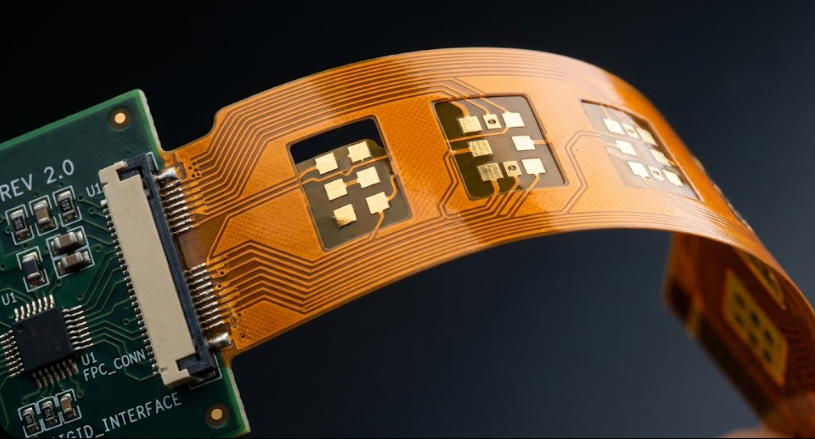
Otherwise, such traces would deteriorate within weeks in the field. We are going to discuss the nature of flex coverlay, why it is important for reliability, how to design around it, and what goes into it to manufacture it correctly today. Designing your first flex circuit, or maximizing a high-volume product, knowing coverlay will make you make smarter material and design decisions.
The Essential Role of Flex Coverlay in Flexible PCBs
One of the most crucial layers in a flex circuit stackup is the coverlay. It has a direct influence on the survival of the board to bending, environmental exposure, and long-term service. A coverlay (also known as a cover layer) is a laminated sheet that is placed over the outer copper layers of a flexible PCB. It is made of two bonded parts: a polyimide (PI) film on the surface and a thermosetting adhesive layer underneath the film that connects the film to the copper surface.
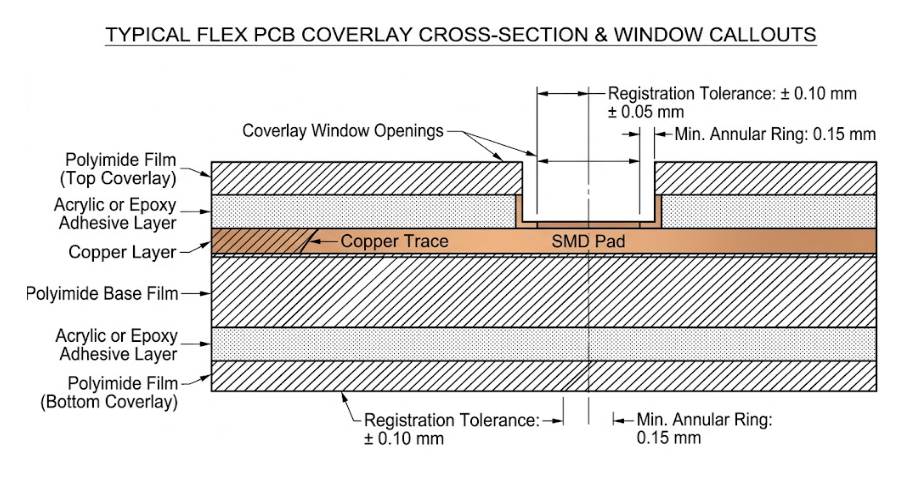
The polyimide is normally 12.5 to 50 micrometers thick, but the most popular is 25 micrometers (1 mil). Another 15 to 25 micrometers is provided by the adhesive layer, typically acrylic or epoxy-based. Combined, total coverlay thickness is between approximately 27.5 and 75 micrometers.
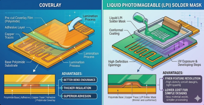
Coverlay is a solid film in contrast to liquid photoimageable (LPI) solder mask on rigid PCBs. This is essential since liquid solder mask is brittle once it has cured, and it breaks when flexed repeatedly. Polyimide coverlay retains its flexibility following hundreds of thousands of bending cycles, so IPC-6013 recommends it as the outermost protection of dynamic flex applications.
Why It Is Critical for Flexible Circuit Reliability
Exposed copper traces are susceptible to multiple failure modes without a ca overlay. Conductivity is reduced by oxidation in wet conditions and eroded by mechanical contact between the housing, trace geometry is eroded by trace contact, and neighboring traces may short due to condensation or contamination. All these threats are handled by Coverlay in one layer.
The polyimide film offers a dielectric barrier of breakdown voltages over 7,000 V/mil, and it is chemically inert to solvents, flux residues, and cleaning agents used during assembly. In dynamic flex applications with continuous bending of the circuit, such as a laptop hinge or a printer head carriage, coverlay is the major structural layer that provides structural integrity to the circuit under cyclic loading.
Key Benefits of Using Flex Coverlay
The substitution of alternative protective layers with coverlay has quantifiable benefits in terms of protection, flexibility, and electrical performance. This is why it is the industry standard.
Superior Protection Against Oxidation and Mechanical Damage
One of the chemically resilient polymers that is employed in electronics is polyimide. It is resistant to oxidation at temperatures up to 260 degrees Celsius and has mechanical properties between minus 65 and plus 300 degrees Celsius. Bonded across copper traces, it forms an almost hermetic seal that excludes moisture and oxygen access to the metal.
Polyimide coverlay has a tensile strength of over 230 MPa, which means it is much stronger in resisting abrasion, puncture, and tearing as compared to liquid solder mask. In systems where the flex circuit slides over a wall of the housing or through a narrow cable guide, this hardness eliminates wear-through, exposing traces.
Improved Bend Endurance and Electrical Insulation
Bend endurance is the largest single benefit of coverlay compared to liquid solder mask. Typical LPI solder mask cracks after a few hundred bend cycles, whereas polyimide coverlay can withstand more than 200,000 dynamic bend cycles at a 5 mm bend radius without cracking or delaminating. This is due to the fact that there are two properties that work together to bring about this endurance. Polyimide is an elastic material with a low elastic modulus in comparison with cured epoxy. Polyimide will not resist the copper, but will deform with it. The acrylic adhesive layer provides a buffer of stress and spreads flexural strain more uniformly.
Polyimide coverlay is electrically suitable with a dielectric constant (Dk) of about 3.2 to 3.5 and a dissipation factor (Df) of about 0.002 to 0.008 at 1 MHz, which is suitable in both low-frequency and moderately high-frequency applications.
| Property | Polyimide Coverlay | LPI Solder Mask (Rigid) |
|---|---|---|
| Typical Thickness | 25 - 75 um | 15 - 30 um |
| Bend Endurance | 200,000+ cycles | Less than 500 cycles |
| Operating Temperature | -65 to +300 C | -40 to +130 C |
| Dielectric Strength | Greater than 7,000 V/mil | 1,000 - 1,500 V/mil |
| Chemical Resistance | Excellent | Moderate |
| Application Method | Lamination (heat + pressure) | Screen printing or spraying |
| Best Suited For | Dynamic and static flex | Rigid boards only |
Design Considerations for Effective Flex Coverlay
Getting the most out of your coverlay requires attention during the design phase. Poor coverlay design is one of the most common causes of flex circuit failures, and most issues are entirely preventable.
Coverlay Window Design and Alignment Rules
Coverlay windows are the areas where the coverlay is removed to expose pads, test points, or connector contacts. Since coverlay is a pre-cut solid film, these openings are created by die-cutting or laser cutting before lamination. This limits feature size and alignment accuracy compared to the PI solder mask. Here are the key design rules:
1.Maintain a minimum coverlay opening of 0.2 mm larger than the pad on each side for alignment tolerance.
2.Keep a minimum overlap of 0.25 mm where the coverlay extends over the trace leading to a pad.
3.Avoid isolated openings below 1.0 mm diameter, as they are difficult to die-cut consistently.
4.Use rounded corners on openings rather than sharp 90-degree angles to prevent tearing.
5.Specify a minimum 0.5 mm coverlay-to-board-edge setback to prevent delamination.
6.For closely spaced pads, use a single large window rather than individual small openings.
Standard alignment tolerances are plus or minus 0.1 to 0.15 mm. High-precision processes can achieve plus or minus 0.05 mm at increased cost.
Material Selection for Different Flex Applications
Not all coverlay materials are the same. Polyimide film grade and adhesive type will depend on your thermal, mechanical, and flexibility needs. General-purpose flex circuits are most often made with acrylic adhesive coverlays with a good degree of flex and a peel strength of 1.0 to 1.5 N/mm, operating at temperatures up to 105 degrees Celsius.
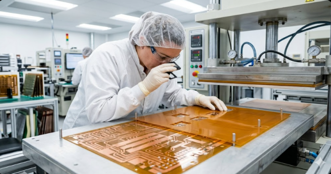
Epoxy adhesive coverlays offer better temperature resistance up to 155 degrees Celsius, which is desired in automotive under-hood or other industrial settings. They are a little harder, and this may decrease the endurance of bends in dynamic applications. Adhesiveless coverlay eliminates the adhesive layer entirely by directly bonding polyimide to copper. This gives it the thinnest profile, maximum temperature, and optimum high-frequency performance. It is normally applied in high-frequency and aerospace flex circuits.
| Adhesive Type | Temperature Rating | Peel Strength | Flexibility | Best Application |
|---|---|---|---|---|
| Acrylic | Up to 105 C | 1.0 - 1.5 N/mm | Excellent | Consumer, wearable, general flex |
| Epoxy | Up to 155 C | 1.2 - 1.8 N/mm | Good | Automotive, industrial |
| Adhesiveless | Up to 300 C+ | Varies | Very Good | Aerospace, high-frequency, HDI flex |
Professional Manufacturing of Flex Coverlay
The performance of coverlay depends just as much on how it is applied as on the material itself. Even the best polyimide film will fail if lamination introduces voids, wrinkles, or adhesion defects.
Precision Application and Curing Processes
The coverlay application process follows a precise sequence:
1.Pre-cutting: The coverlay sheet is die-cut or laser-cut to match the panel layout with all pad openings.
2.Surface preparation: Copper is cleaned and micro-etched to improve adhesive bonding.
3.Alignment and tacking: Pre-cut coverlay is aligned using registration pins or optical systems and tacked in place.
4.Lamination: The assembly enters a vacuum press at 160 to 190 degrees Celsius, 15 to 30 kg/cm2, for 30 to 90 minutes.
5.Post-cure: Some adhesives require additional oven curing for full crosslinking.
6.Inspection: Panels are checked for voids, wrinkles, delamination, and alignment accuracy.
Vacuum lamination is preferred because removing air from the chamber ensures the coverlay conforms to etched trace valleys without trapping bubbles that would become delamination initiation points.
Quality Control for Adhesion and Uniformity
The most important quality measure is adhesion testing. According to IPC-TM-650, peel strength is determined by pulling the overlay off the copper surface at 90 degrees. The lowest acceptable level is 0.8 N/mm w, with the best processes being 1.2 N/mm or more.
Uniformity checks ensure that there is uniform thickness throughout the panel and that there is a good flow of adhesives. The difference in thickness must remain within a percentage of 10. Adhesive fill between traces is confirmed by cross-sectional microscopy and proves that no voids exist. Other quality checks are:
- Wrinkles, bubbles, or discoloration: Visual inspection.
- Checking of openings against design information.
- Thermal stress (solder float 288 degrees Celsius, 10 seconds IPC-TM-650)
- Bend testing of dynamic flex applications to verify flex life is within specifications.
JLCPCB's Expertise in Flex Coverlay Production
Advanced Coverlay Application and High-Precision Processing
JLCPCB has specific flex PCB production lines with vacuum lamination presses that are set to coverlay. The vacuum technique removes any trapped air and provides a uniform flow of adhesive, even on thick multi-trace designs where lamination without a void is difficult.
Precision laser systems deal with coverlay cutting of narrow-tolerance openings, especially when dealing with fine connector regions. The accuracy of registration is held to within 0.1 mm plus or minus, and is suitable for most commercial flex designs.
DFM Support for Optimal Flexible PCB Performance
DFM review is one of the most useful features of collaboration with JLCPCB that can identify coverlay defects prior to production. Popular problems reported are:
- Coverlay apertures that are too near the pad edge, potentially obstructing partially.
- Lack of coverlay overlap on trace entries to pads.
- Coverlay windows with sharp ends that may start tearing.
- Less than adequate coverlay-to-edge clearance that could cause delamination.
Such an initiative check saves you the money and time wasted in making post-fabrication discoveries. The DFM feedback is real-world training in the rules of coverlay design to engineers unfamiliar with flex design.
Reliable High-Volume Manufacturing with Consistent Quality
JLCPCB uses the same process controls whether you are ordering 5 prototype flex PCBs or 10,000 units. Incoming coverlay material is checked in terms of thickness, adhesive properties, and shelf life. Lamination temperature, pressure, and time of laminating are monitored in-process and per panel.
Final inspection is done according to IPC-6013 standards of flexible printed circuit qualification. Your flex designs can be easily put into production with competitive prices and 1-2 day lead times on standard orders. When designing a flexible circuit and you need to be sure that your coverlay is placed in the right location on the first build, the flex PCB service at JLCPCB is capable of using its materials experience, accuracy in equipment, and quality checks to produce the desired results.
FAQ
Q: What is flex coverlay?
Flex coverlay is a laminated protective film applied over the outer copper layers of a flexible PCB. It consists of a polyimide film bonded with a thermosetting adhesive layer, providing insulation, environmental protection, and mechanical durability during bending.
Q: What is the difference between coverlay and solder mask on flex PCBs?
Coverlay is a pre-cut solid polyimide film laminated under heat and pressure. Solder mask is a liquid coating applied by screen printing or spraying. Coverlay survives repeated bending, while liquid solder mask cracks after relatively few bend cycles.
Q: Can I use liquid solder mask instead of coverlay on a flex PCB?
For static flex applications bent once during installation, a liquid solder mask can sometimes work. For dynamic flex involving repeated bending, coverlay is strongly recommended as LPI solder mask cracks within a few hundred cycles.
Q: What is the typical thickness of flex coverlay?
The most common construction is 25 micrometers of polyimide plus 25 micrometers of adhesive, totaling 50 micrometers. Options range from about 27.5 to 75 micrometers total, depending on protection requirements.
Popular Articles
• Design Guidelines for Flex PCB Panels on JLCPCB
• 45 Must-Know Flex PCB Design Tips You Can't Afford to Miss!
• Essential Design Guidelines for Flex PCBs
• FPC Design Rules: 13 Safety Distances You Can’t Ignore
• Mastering PCB Stiffeners: A Comprehensive Guide to Types, Applications, and Design Best Practices for Flexible Circuits
Keep Learning
Flex PCB Designing Useful Tips - JLCPCB
Flexible printed circuit boards, or Flex PCBs, are thin, lightweight printed circuit boards that can be bent, folded, and twisted to fit into any shape or size without damaging the electrical connections on the board. Flex PCBs are becoming increasingly popular in various industries, such as aerospace, automotive, medical devices, and consumer electronics. In this article, we will discuss what to consider while designing a Flexible PCB for effective product development. Currently, flex PCB manufacturi......
Flex PCB Manufacturing Process & Advantages
In today's fast-paced and technologically advanced world, printed circuit boards (PCBs) have become an integral part of many electronic devices. However, with the increasing demand for smaller and more flexible electronic devices, the traditional rigid PCBs are proving to be less efficient. This is where Flexible Printed Circuit Boards (Flex PCBs) come in, providing much-needed flexibility while maintaining the same level of functionality as rigid PCBs. For new users, JLCPCB also prepared up to $70 re......
Design Guidelines for Flex PCB Panels on JLCPCB
When placing orders for flexible PCBs (FPCs) on JLCPCB, several key points must be noted. Unlike rigid PCB panels, which often use mouse bites or V-cuts for depanelization, FPC panels require bridge (tab) connections. Requirements for Flex PCB Panels on JLCPCB FPC panelization differs significantly from rigid boards. Proper design ensures efficient manufacturing, high yield, and compatibility with SMT assembly. Key requirements are as follows: Internal Board Spacing: 2 mm (standard); preferably 3 mm w......
Flexibility and Reliability: Exploring the World of Flexible PCB
Key Takeaways Flexible PCBs deliver unmatched flexibility and reliability, making them essential for modern compact and dynamic electronic designs. With high-performance polyimide substrates, 1-4 layer configurations, ultra-thin 25μm options, and precision 2/2mil traces, JLCPCB’s Flexible PCBs excel in space-saving, weight reduction, and repeated bending applications across consumer electronics, medical devices, wearables, automotive, and aerospace industries. Whether choosing pure flex or rigid-flex ......
Avoid Trace Fractures in Flexible PCB Design
Flexible PCBs, also known as Flex PCBs, have gained immense popularity in the field of electronics due to their exceptional flexibility and versatility. These boards offer unique advantages, enabling efficient electrical signal transmission while withstanding bending and movement. However, when designing flexible PCBs, one crucial aspect that engineers and designers must consider is the prevention of trace fractures. Trace fractures can lead to significant issues such as signal loss, intermittent conn......
Exploring Flexible PCB: Applications and Design Considerations
Key Takeaways Flexible PCBs (flex circuits) are revolutionizing modern electronics with their superior flexibility, lightweight design, and space-saving capabilities. From wearable devices and automotive systems to aerospace applications and foldable consumer electronics, they enable innovative form factors that rigid boards cannot achieve. Successful flexible PCB design hinges on critical factors including proper bend radius, optimized trace/space width, strategic component placement with stiffeners,......