
Avoid PCB Assembly Failures: Mastering Solder Mask Expansion Rules and Best Practices
6 min
- Introduction: Why Solder Mask Expansion is Critical for PCB Reliability
- Standard Values and Core Concepts of Solder Mask Expansion
- Design Rules and Best Practices for Optimal Solder Mask Expansion
- Manufacturing Challenges and Professional Solutions for Solder Mask Expansion
- Impact of Expansion on Soldering Yield and Long-Term Reliability
- Conclusion: Achieve Perfect Solder Mask Results with Professional Expertise
- FAQ: Common Questions About Solder Mask Expansion
Solder mask protects copper traces and pads from oxidation, bridges, and contamination during assembly. Incorrect solder mask expansion—the clearance around features where mask is pulled back—leads to defects like shorts or exposed copper. Engineers must set expansion values precisely to ensure reliable soldering and long-term performance.
Introduction: Why Solder Mask Expansion is Critical for PCB Reliability
Understanding Solder Mask and Expansion Basics
Solder mask is a polymer layer applied over the PCB to insulate copper except at solderable areas. Expansion defines how much the mask opening extends beyond the pad or trace edge, typically 0.05–0.1 mm per side. This accounts for registration tolerances during mask alignment and prevents mask from encroaching on pads. In liquid photoimageable (LPI) masks, common in professional fabrication, expansion ensures clean openings after exposure and development.
How Poor Expansion Leads to Assembly Issues
Insufficient expansion causes mask to overlap pads, leading to poor solder wetting or dry joints. Excessive expansion exposes traces to oxidation or shorts from solder bridges. In high-density designs, these issues increase rework costs and failure rates by 20–30%. Proper expansion also aids in wave soldering by controlling solder flow and reduces tombstoning in reflow.
Standard Values and Core Concepts of Solder Mask Expansion
Clearance, Overlap, and Expansion Definitions
Clearance is the distance from pad edge to mask edge, positive for expansion (mask pulled back) or negative for overlap (mask covers edge). Overlap protects fine traces from etchant but risks assembly if too large. Expansion values balance manufacturing tolerance (alignment accuracy ±0.05 mm) and assembly needs, with clearance ensuring at least 0.025 mm exposed copper ring for solder fillet formation.
Industry Standards and Recommended Values
IPC-7351 recommends 0.05–0.075 mm expansion for SMD pads and 0.1 mm for through-hole. For vias, tenting (full coverage) or plugging uses zero or negative expansion. In high-reliability boards, adjust for mask type—LPI allows tighter 0.05 mm vs. dry film at 0.075 mm.
| Feature Type | Recommended Expansion (mm) | Tolerance Consideration | Notes |
| SMD Pads | 0.05–0.075 | ±0.025 | Ensures wetting without bridges |
| Through-Hole Pads | 0.1–0.15 | ±0.05 | Accommodates annular ring |
| Traces | 0.025–0.05 | ±0.025 | Prevents exposure in fine lines |
| Vias (Untented) | 0.05–0.1 | ±0.05 | Allows plugging if needed |
| BGA Pads | 0.025–0.05 | ±0.025 | Tight for fine pitch |
Table 1: Standard solder mask expansion values by feature type.
These values derive from IPC standards and fabrication capabilities, where tighter tolerances require advanced alignment.
Design Rules and Best Practices for Optimal Solder Mask Expansion
Rules for Pads, Vias, Traces, and High-Density Areas
For SMD pads, set expansion to 0.05 mm to expose enough copper for solder fillet while avoiding bridges in 0.5 mm pitch. Vias need 0.1 mm if untented to prevent solder wick, or zero for tenting to block ingress. Traces require minimal 0.025 mm to protect from etchant without narrowing effective width. In high-density areas, scale expansion down to 0.025 mm for 0.4 mm pitch, but verify with DFM to match fabrication limits.
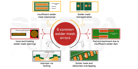
Common Pitfalls and How to Avoid Them (Slivers, Bridging)
Slivers occur when expansion creates thin mask strips (<0.1 mm) that peel during curing—avoid by increasing clearance or merging openings. Bridging happens with negative expansion on close pads—use dams (0.1 mm wide mask strips) between pads. Check Gerber files for mask misalignment risks, and use teardrops on vias to enhance adhesion.
Special Cases: SMD Pads, BGA, and High-Density Designs
BGA pads demand NSMD (non-solder mask defined) with 0.05 mm expansion for better alignment tolerance. SMD pads favor SMD (solder mask defined) with slight overlap for protection. High-density designs integrate dams to prevent solder flow between fine-pitch pads, ensuring 0.075 mm min dam width for reliable curing.
Manufacturing Challenges and Professional Solutions for Solder Mask Expansion
Impact of Expansion on Soldering Yield and Long-Term Reliability
Tight expansion improves yield by ensuring clean pad exposure for HASL or ENIG finishes, but too small risks incomplete development, leaving residue that causes poor wetting. Over time, insufficient expansion exposes copper to humidity, accelerating corrosion. Optimal values support reflow profiles with peak 260°C, reducing voids by 15–25%.
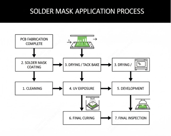
Advanced Process Controls in Professional Fabrication
Professional processes use LPI mask with 0.01–0.03 mm thickness for high resolution. Exposure aligns to ±0.025 mm using laser imaging, and development removes unexposed areas precisely. Curing at 150°C hardens the mask without shrinkage. Multi-color options (green, black, blue) affect thermal properties, with matte finishes reducing glare in inspection.
How Expert Manufacturers Handle Expansion Tolerances and Variations
Fabricators control tolerances through automated coating and double-sided application for uniformity. Test coupons verify expansion on each panel. Variations from board thickness or copper density are mitigated with adaptive exposure. DFM reviews adjust for 4-layer vs. multilayer, ensuring 0.05 mm min for high-density.

Conclusion: Achieve Perfect Solder Mask Results with Professional Expertise
Solder mask expansion is key to avoiding shorts, poor joints, and corrosion. Use 0.05–0.1 mm for most pads, scale for density, and follow IPC for reliability in consumer or industrial boards.
JLCPCB excels in precise solder mask application with LPI technology, achieving ±0.025 mm alignment and 0.01–0.03 mm thickness. Their multi-color options (green, black, white, blue, red) suit various needs, with matte finishes available. Quick-turn prototyping lets you test expansion settings, and free DFM checks catch issues early. Upload designs at jlcpcb.com for instant quotes and fabrication that ensures assembly success.

FAQ: Common Questions About Solder Mask Expansion
Q1: What is the ideal solder mask expansion for SMD pads?
A: 0.05–0.075 mm per side to ensure good solder wetting without risking bridges; adjust based on pitch and IPC guidelines.
Q2: How does negative expansion affect PCB reliability?
A: It provides overlap for trace protection but can cause poor wetting if too large (>0.05 mm); use sparingly on fine pads to avoid assembly defects.
Q3: Why use dams in high-density designs?
A: Dams (0.1 mm wide mask strips) prevent solder bridging between close pads; minimum width ensures curing stability.
Q4: Can solder mask expansion vary by mask color?
A: No, but multi-color options affect visibility and thermal properties; green is standard, black suits high-contrast inspection.
Keep Learning
Conformal Coating in PCB Technology: Benefits, Challenges, and Future Developments
If you're searching for conformal coating, you're likely looking for a reliable way to protect your PCB from moisture, dust, chemicals, or harsh environments. Choosing the right coating directly affects product reliability, performance, and lifespan. In this guide, you'll learn what conformal coating is, the main types available, and how to select the best option for your application. We'll also cover key benefits, application methods (manual, automated, and selective), as well as inspection, rework, ......
Preventing Black Pad Defects: Ensuring Reliable ENIG Finish in Professional PCB Manufacturing
Key Takeaways Black Pad is caused by excessive nickel corrosion during the ENIG immersion gold step, leading to brittle solder joints and hidden BGA/QFN failures. Key prevention methods: tight chemistry control (temperature, pH, time), consistent phosphorus content, and regular bath monitoring. High-reliability alternatives: ENEPIG (lowest risk) or nickel-free finishes like Immersion Silver and OSP. Always source ENIG from manufacturers with strict process controls. Ever get a great-looking board, wor......
Solder Mask Colors: Boost Your PCB Performance, Style & Reliability
Key Takeaways Solder mask color directly impacts AOI accuracy, thermal performance, and PCB reliability — it is not purely cosmetic. Green remains the industry benchmark for the highest manufacturing yields and fastest turnaround at no extra cost. White maximizes light reflection for LED applications, while black offers a premium aesthetic for high-end consumer products. Red and yellow provide superior visual contrast for prototyping, debugging, and safety-critical inspections. JLCPCB offers all seven......
Why Copper Oxidation Matters in PCB Design & How to Prevent It
Key Takeaways Copper oxidation is a critical concern in PCB design that directly impacts solderability, contact resistance, and long-term reliability. By understanding how oxidation forms and damages copper surfaces, designers can effectively prevent it through appropriate surface finishes (such as HASL, ENIG, and OSP), strategic solder mask application, and strict adherence to proper storage and handling practices per IPC-1601 guidelines. Protecting copper from oxidation ensures better assembly yield......
Comparing OSP Plating with Other PCB Surface Finishes
Key Takeaways OSP stands out as a cost-effective, ultra-flat, and environmentally friendly PCB surface finish with excellent solderability for fine-pitch components, making it ideal for high-volume consumer electronics. However, its short shelf life (3–6 months), sensitivity to handling and oxidation, and limited multi-reflow durability require careful storage and process control. When compared to HASL, ENIG, Immersion Silver, and Immersion Tin, OSP offers superior planarity and lower cost but trades ......
Hard Gold PCB Finish: Achieving Exceptional Wear Resistance and Contact Performance
Surface finishes are not all the same thing, and this is obvious beyond mention when you are dealing with parts that are beaten against one another over and over. Hard gold. The most common finish used when PCBs must complete hundreds or even thousands of insert-and-remove operations before going out of service is essentially a hard alloy of gold electroplated over a nickel barrier coating. The prototypical piece of evidence that demonstrates why this is important is the edge connector, otherwise know......