
How Design Rule Check Prevents Expensive PCB Production Mistakes
14 min
- Why Design Rule Check Is Critical for Every PCB Project
- Key DRC Rules Every Designer Must Master
- Running Effective Design Rule Checks in Your Workflow
- How Professional Manufacturing Benefits from Strong DRC
- JLCPCB's Advanced DRC and DFM Expertise
- Frequently Asked Questions (FAQ)
Have you ever sent Gerber files to your fab house, and you can get an email back saying that they need to fix clearance or annular ring issues, and only then can they start production? When that comes out like you, you know how frustrating that can be, days wasted, revision numbers rising, shipping dates falling. Catching all of that is actually the real MVP of good design, which is a solid design rule check in your PCB layout tool, that allows you to discover all of that before it even leaves your desk.
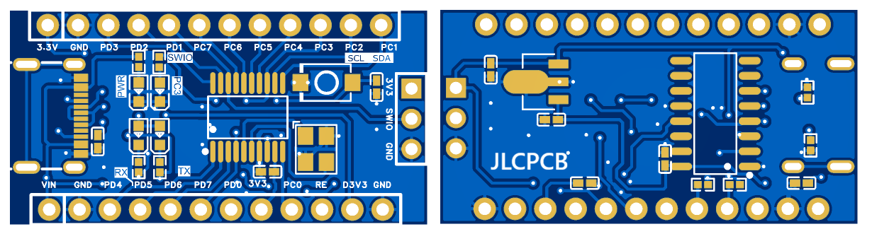
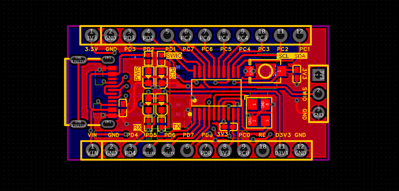
This becomes important even more on narrow boards. Consider a small, 34.9mmx17.9mm, CH32V003 dev board, containing 35 nets, 41 through vias, and 29 components. With that kind of little board you have to squeeze everything on, every other mil of clearance counts. Add one more violation in the USB input section or between the crystal nets PA1/PA2 and the MCU core, and what would otherwise have been a fast prototype can soon turn into an expensive re-spin.
I will show you today how DRC really works, what rules you actually must be a master of, when to do checks in the flow of your design, and how clean DRC files can be converted into cheaper, quicker manufacturing. This guide is going to hone your process, whether you are laying out your first 2-layer board or just polishing a production design.
Why Design Rule Check Is Critical for Every PCB Project
Understanding DRC’s Role in Modern Design Flows
A Design Rule Check is the automated guardrail that sits between your creative layout work and the physical reality of PCB fabrication. Every fab house operates within a set of manufacturing constraints: minimum trace widths, minimum spacing between copper features, smallest reliable drill diameter, and required annular ring sizes. DRC takes those constraints and turns them into enforceable rules inside your EDA tool.
Think of DRC as a translator. It converts the fab shop's capability sheet into a digital ruleset that your layout editor can check against every trace, pad, via, and clearance on your board. When you route a trace too close to a via on your CH32V003 board's dense MCU core area, DRC flags it immediately rather than letting it slip through to production.
Here is the critical point that many designers miss: DRC is not a one-time final check. You should run it after floorplanning, during routing of each functional block, and again before Gerber release. Each pass catches different categories of errors at the stage where they are cheapest to fix.
The High Cost of Skipping DRC in Production
Violations that slip past design review become physical defects at the fabrication or assembly stage. A clearance violation between the D+//- USB differential pair and an adjacent ground pour might not look like much on screen. But at the fab house, that violation can result in copper shorts after etching, turning finished panels into scrap.
On compact boards like the CH32V003 reference design, these problems surface fast. With 29 components packed into roughly 630 square millimeters of board area, the margin for error on solder mask slivers and copper clearances is razor-thin. A mask opening that barely passes on a larger board becomes a guaranteed defect here.
Skipping DRC also delays first-article approval. Many designers assume their layout is clean because the routing was completed without obvious errors. But fabricators run their own DFM checks on your Gerbers, and when they find issues, your order goes on hold. That hold can add 3 to 5 days to a run that was supposed to ship in 48 hours.
Key DRC Rules Every Designer Must Master
Clearance, Spacing, and Annular Ring Requirements
Clearance rules are similar to the rudimentary rules you have to abide by when configuring a DRC. You need to establish the minimum spacing between all the copper parts, trace to trace, trace to pad, pad to via, and even copper to the edge of the board. In the case of a typical 2-layer board used by mainstream fabs, a clearance of 0.2mm (approximately 8mil) typically suffices. When you are on the edge, many fabs can do 0.1mm (4mil), though you need to keep a close watch on your etchant and imaging process.
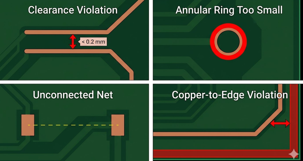
An annular ring is the copper ring that remains on a hole that has been drilled in the board when it is made. When the drill jack starts a little, the annular ring may become too small, and the pad will lose its attachment. Class IPC-6012 Class 2 states that internal layers (as well as external layers) require a minimum annular ring diameter of 0.05 mm (2 mil), but it is a safer practice to have 0.15 mm (6 mil) on external layers, which is likely to guarantee reliable production.
Do not forget the copper to board edge clearance. According to IPC-2221, copper must not be brought closer than 0.25mm to the edge of the board to prevent separation of copper due to routing. In the CH32V003 board, this is to be double-checked, particularly around the USB connector, where traces are running close to the board perimeter.
| DRC Rule | Safe Default (2-Layer) | Advanced Capability | IPC Reference |
| Trace-to-trace clearance | 0.2 mm (8 mil) | 0.1 mm (4 mil) | IPC-2221 |
| Trace-to-pad clearance | 0.2 mm (8 mil) | 0.1 mm (4 mil) | IPC-2221 |
| Annular ring (external) | 0.15 mm (6 mil) | 0.075 mm (3 mil) | IPC-6012 |
| Copper-to-board edge | 0.25 mm (10 mil) | 0.2 mm (8 mil) | IPC-2221 |
| Solder mask sliver | 0.1 mm (4 mil) | 0.05 mm (2 mil) | IPC-7525 |
Trace Width, Via Rules, and Copper Balance Guidelines
The width of traces is determined by two primary factors, namely the current-carrying capability and the ease of manufacture. A width of 0.15 mm (6 mil) suffices for signal traces on the CH32V003 board that are only pulled in a few milliamps. The 3V3 power rail supplying the MCU and the USB-to-TTL converter must have broader traces, however. Current up to 500 mA on a 1 oz copper outer-trace with moderate temperature increase can be done well with a width of 0.3 mm to 0.5 mm.
Via rules constrain the drill diameter and the finished hole-to-pad ratio. A standard through-hole via with a 0.3 mm drill and a 0.6 mm pad provides a healthy annular ring and reliable plating. Your CH32V003 board uses 41 through vias, so consistent via sizing helps the fab optimize its drill program and improves plating uniformity across the panel.
Copper balancing is a rule that often gets overlooked in DRC but has a real manufacturing impact. When one side of a 2-layer board has significantly more copper than the other, the board tends to warp during lamination and reflow. On your compact CH32V003 board, ensure that if you have a ground pour on the bottom layer, you also have reasonable copper coverage on the top layer. This reduces warpage and improves etch uniformity.
| Via Parameter | Standard Value | Notes |
| Drill diameter | 0.3 mm (12 mil) | Most common for signal vias |
| Pad diameter | 0.6 mm (24 mil) | Provides a 0.15 mm annular ring |
| Aspect ratio (board thickness: drill) | 8:1 max | For reliable plating on 1.6 mm boards |
| Via-to-via spacing | 0.5 mm (20 mil) | Prevents drill breakout between adjacent vias |
| Via-to-trace clearance | 0.2 mm (8 mil) | Match the net class clearance minimum |
Running Effective Design Rule Checks in Your Workflow
Setting Custom Rules and Running DRC at Key Stages
Running DRC at the right moments is just as important as having the right rules defined. Here is the three-stage workflow that works well for boards like the CH32V003 reference design:
- Post-Floorplan DRC: Run immediately after placing components, defining the board outline, and setting up your layer stack and design rules. At this stage, you are checking courtyard overlaps, component-to-edge clearances, and net class rule definitions. On the CH32V003 board, this catches issues like the USB connector footprint extending beyond the board edge or component courtyards overlapping in the dense MCU core zone.
- Block-Level DRC: Run after completing routing for each functional block. Route the power section (3V3 regulator, input decoupling) first, run DRC, then route the clock network (crystal nets PA1/PA2), run DRC again, then tackle the USB D+/- pairs, the SWIO debug interface, and the GPIO/programming header. Each check ensures the current block is clean before you add routing complexity from the next block.
- Final Full-Board DRC: Run a complete DRC with all rules active before generating Gerber files, the bill of materials, and the component placement list (CPL). This is your last opportunity to catch cross-block interactions: a power trace routed in Stage 2 that now violates clearance against a signal trace added in Stage 2's clock routing, for example.
Setting custom rules for each stage prevents false positives. During Stage 1, you might disable routing-specific checks (trace width, via rules) since no traces exist yet. By Stage 3, every rule should be active with no exceptions.
Interpreting Reports and Prioritizing Critical Fixes
A DRC report on a moderately complex board can return dozens of violations. Not all violations carry the same weight. Prioritizing them correctly saves time and ensures you fix the problems that actually block manufacturing before spending effort.
Prioritize violations in this order:
1.Hard manufacturing blockers: These include copper shorts, clearance violations below the fab's minimum capability, annular ring violations, and unconnected nets. On your CH32V003 board with 35 nets and 0 unrouted nets, an unconnected net appearing in the DRC report means something broke during editing and needs immediate attention.
2.Reliability risks: Silkscreen overlapping exposed pads, solder mask slivers between closely spaced pads, and weak thermal reliefs on ground plane connections. These will not necessarily stop fabrication, but they cause assembly defects and reduce long-term reliability.
3.Cosmetic and advisory warnings: Slightly wider trace-to-trace spacing than your preferred value, text placement recommendations, and copper balance advisories. Fix these when time allows, but do not hold up a production release for them.
Keep a waiver log for any violations you intentionally accept. If you deliberately place a via closer than the default minimum to a pad in the NRST reset circuit because the routing topology demands it, document the exception with the actual measured clearance and your engineering justification. This log becomes invaluable when a different engineer reviews the design or when you revisit the board months later.
How Professional Manufacturing Benefits from Strong DRC
Reducing Revisions and Production Delays
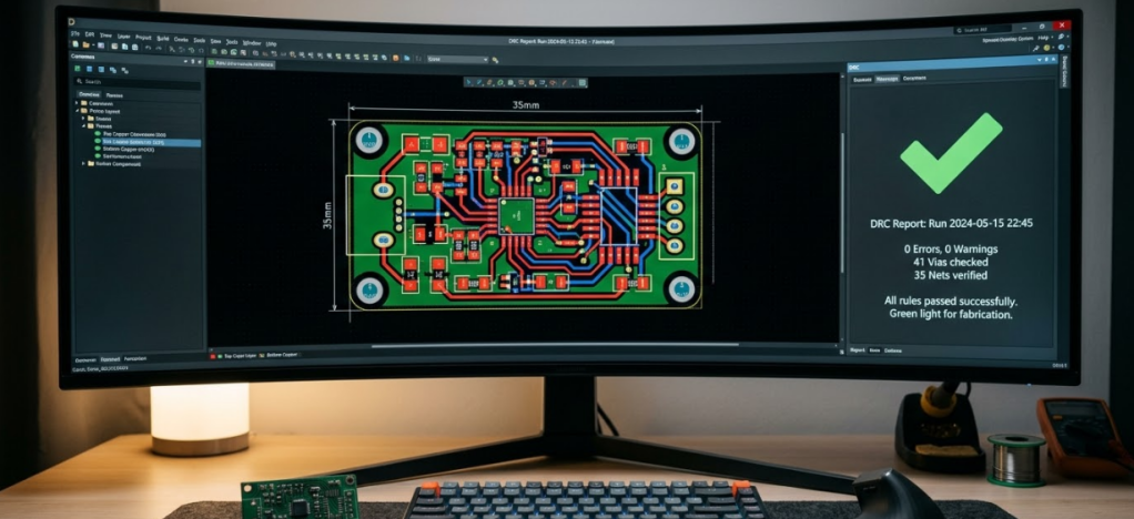
When your Gerber files arrive at the fabricator with zero DRC violations, the CAM engineering team can approve them faster. There are no questions to ask, no "engineering hold" emails, and no back-and-forth about whether a tight clearance was intentional or accidental. For fast-turn prototype services that promise 1 to 2 day production times, a clean file set is the difference between hitting that timeline and missing it. DRC-clean designs also reduce revision counts. Every board spin costs money, not just in fabrication fees, but in engineering time, component procurement delays, and schedule risk.
On a compact board like the CH32V003 design, where the layout is tight but not exceptionally complex, there is no reason to accept avoidable re-spins caused by missed DRC violations. Modern PCB manufacturers like JLCPCB process thousands of designs daily. Boards that pass DFM screening without flags move straight into the production queue. Boards with issues get flagged for manual review, and that review takes time. A strong DRC discipline on your end directly translates to faster turnaround on the fab side.
Improving Yield and Lowering Overall Costs
Clean drill files, well-defined copper geometries, and properly sized mask openings directly improve fabrication yield. When every via has an adequate annular ring, the drill-to-pad registration tolerance is forgiving. When every trace meets the minimum width, the etching process produces consistent results across the panel. On the assembly side, correct solder mask openings and accurate pad geometries reduce solder bridging, tombstoning, and insufficient solder defects.
For the CH32V003 board with its mix of fine-pitch IC pads and through-hole connectors, these geometry details matter for first-pass assembly yield. The cost impact compounds at volume. Even a 2 percent yield improvement on a 1,000-board run saves 20 boards worth of material, assembly time, and rework labor. Over multiple production runs, the cumulative savings from DRC-clean designs are substantial. Less rework means lower effective per-board cost and reduced schedule risk for every order.
JLCPCB's Advanced DRC and DFM Expertise
Built-in DRC Validation for Fast, Reliable Feedback
DRC, your design is a built-in feature of your CAD that compares your design to the rules that you specify. But what of the rules you did not consider? It is there that a second layer of validation of DFM external is provided. JLCDFM can be downloaded free of charge and is offered by JLCPCB. This analysis is done on your Gerber files and compares them with the actual production lines they can produce.
JLCDFM identifies issues that exceed normal DRC: acid traps in acute-angle trace junctions, too-narrow copper slivers that cannot be etched reliably, drill hits too close to the board edge, and solder mask dams too thin to support the processing. These are the types of problems that a generic CAD DRC lacks, as it is unique to the actual manufacturing process.
A second opinion based on actual production data is running JLCDFM after your CAD DRC. In the case of the CH32V003 board, this comes in handy particularly when checking the narrow spaces between pads of the USB connector and the fine footprint of the MCU. Imagine it like a spell checker and a copy editor: each of them corrects mistakes, but they correct different types of mistakes.
Seamless Transition from Design to High-Quality Fabrication
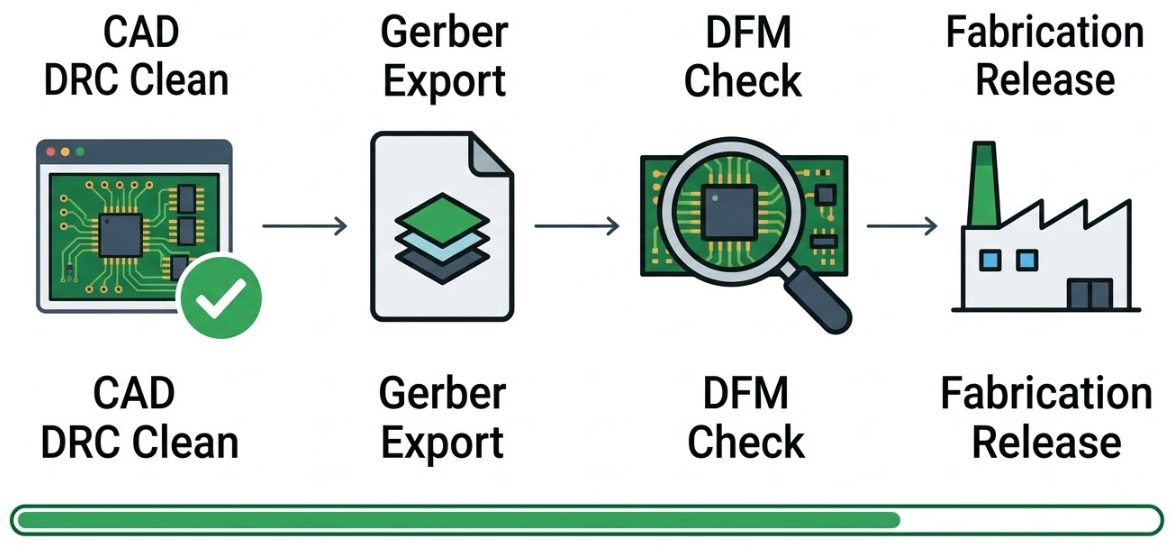
The best approach to PCB class, however, is to make it simple: lock up your layout, run a CAD DRC till it is clean, generate Gerber and drill files, go to JLCDFM, fix whatever comes up, and send it out to be fabricated. This two-step validation will capture nearly all the manufacturability glitches before the board even reaches the factory queue. On the CH32V003 board, it is ridiculously simple to repeat and repeat. Each time you make a change to the schematic, or work on the layout, or change parts, you just repeat the steps.
JLCPCB is the place to go since they have quick prototype turnaround, starting at $2 on standard boards, and in-house DFM tools that simplify the entire process of validation and build. They also do SMT assembly and can produce as fast as 1 -2 days. Therefore, the time lag between a clean design file and a real tested board is never less than before.
Frequently Asked Questions (FAQ)
Q1: Which DRC errors are absolute blockers for fabrication?
Copper shorts, net clearance violations below the fab's minimum capability, annular ring violations that risk losing pad connections after drilling, and unconnected nets are all hard blockers. Any of these will either cause the fabricator to reject your files or result in non-functional boards.
Q2: How should I set initial clearance/width/via rules for a small 2-layer MCU board?
Start with 0.2 mm (8 mil) minimum clearance, 0.15 mm (6 mil) minimum trace width for signals, 0.3 mm (12 mil) minimum trace width for power nets, and a via drill of 0.3 mm with a 0.6 mm pad. These values work reliably with most mainstream PCB fabricators.
Q3: Is CAD DRC alone enough, or should I also run external DFM checks?
CAD DRC checks your design against the rules you defined. External DFM tools like JLCDFM check your Gerber output against actual manufacturing process constraints, including acid traps, copper slivers, mask dam widths, and drill-to-edge distances.
Q4: How often should DRC be run during iterative routing?
Run DRC after each major routing block is completed. On the CH32V003 board, that means after routing the power section, after the crystal and clock nets, after the USB interface, and after the GPIO and programming headers. A final full-board DRC before Gerber export catches any cross-block interactions.
Keep Learning
Etched FPC: Manufacturing Process, Advantages, Applications, and Selection Guide
Ever noticed that thin, amber-coloured ribbon running between the boards in a smartphone camera module or a notebook's lid? That ribbon is almost surely an etched FPC, a flexible printed circuit that's created by chemically removing the unwanted copper to create a precise conductive pattern. It's one of the workhorses of modern electronics, and most people are unaware of the amount of engineering that goes into it. There are more than one flavor of flexible circuit, and the method of manufacture affec......
The Critical Role of Copper Peel Strength in Durable PCB Performance
Key Takeaways Standard Test: Measured via the IPC-TM-650 90° pull test in N/mm. Core Function: Prevents pad lifting and delamination under thermal stress and CTE mismatch. Foil Types: ED foil provides higher adhesion; RA foil yields lower signal loss. Material Benchmarks: Standard FR4 averages 1.0–1.4 N/mm, while High-Tg FR4 achieves 1.2–1.6 N/mm. Design Tips: Add teardrops, eliminate unsupported copper slivers, and perform DFM checks. Ever wonder what's making the copper stay put on your circuit boar......
How Modular PCB Design Simplifies Complex Electronics Projects
Key Takeaway Modular PCB design simplifies complex electronics by breaking boards into independent, reusable functional blocks with clear interfaces. It boosts reusability, speeds up debugging, enhances team collaboration, and reduces errors.Shift from flat to modular design for faster development and more scalable, reliable PCBs. Ever seen a 400+ component schematic and got your head scrambled before even beginning routing? You are not alone. With the ever-increasing density of electronics combined w......
Your Ultimate Guide to PCB Rulers
In the world of PCB design and manufacturing, having the right tools is crucial for achieving accuracy and precision. One such tool that has gained popularity among professionals and hobbyists is the PCB ruler. This specialized measuring tool is designed to provide accurate measurements, reference information, and component footprints, assisting designers, engineers, technicians, and assemblers in various stages of PCB development. In this guide, we'll explore what a PCB ruler is, the features and mea......
Understanding the Materials Used in PCBs: Selection, Types, and Importance
Key Takeaways FR-4 is the go-to material for most cost-effective and reliable PCBs. Use Rogers for high-frequency and RF applications to reduce signal loss. Higher copper weight (2oz) improves current and heat handling. Choose High-Tg substrates for better thermal stability in multilayer boards. Green LPI soldermask offers the best balance of performance and inspection. Printed circuit boards (PCBs) are an essential component of modern electronics. These boards connect and support electronic component......
How to Select Tg of PCB ?
What is the Tg of PCB? In PCB manufacturing, "Tg" stands for Glass Transition Temperature. It is the temperature at which the PCB substrate material transitions from a rigid, glassy state to a soft, rubbery state. PCBs are flame-retardant (UL94 V-0) and do not burn easily; instead, they soften above Tg. The Critical Correlation Between Tg and Z-Axis CTE (Coefficient of Thermal Expansion) When the temperature exceeds the Tg point, the PCB substrate material (such as standard FR-4) undergoes a physical ......