How Copper Foil Shapes PCB Performance and Manufacturing Quality
17 min
- What Is Copper Foil and Why Is It Important in PCBs?
- Understanding Copper Foil in PCB Applications
- Main Types of Copper Foil Used for PCBs
- Copper Foil Uses and Properties That Affect PCB Performance
- Copper Foil Selection and PCB Manufacturing Requirements
- How PCB Manufacturers Control Copper Foil Quality
- FAQ About Copper Foil in PCBs
- Conclusion
Key Takeaways
- Weight: 1 oz copper ≈ 35 µm thickness; higher weight increases current capacity.
- Types: ED for standard rigid boards, RA for dynamic flex circuits.
- DFM & Loss: Smoother foil lowers RF loss; thicker foil requires wider trace spacing.
The part of a PCB that actually carries the electrical signal is the copper foil. The strength comes from the glass weave, the resin is used to keep the layers together, and the solder mask is used to provide protection and separation of exposed copper. But with many designs, copper begins (and ends) with a simple selection in the stack-up: 1 oz.
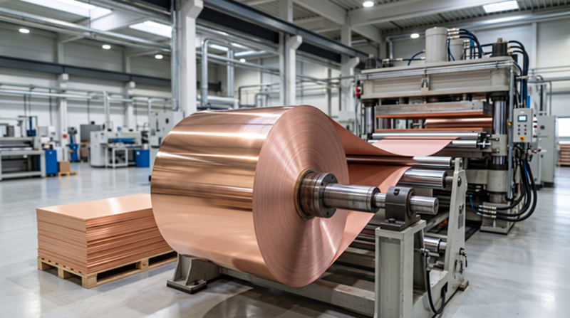
Figure 1: Roll of electrodeposited copper foil feeding into a copper clad laminate press
The majority of PCB copper is a subtractive process. The fabricator begins with a continuous strip of copper that is attached to the laminate and removes all of the copper that is not part of the circuit pattern. This means that there are already certain key characteristics in the copper thickness, grain structure, and surface texture of your Gerber files before they get to production.
All of those properties have an impact on the end product. This guide will discuss the nature of PCB copper foil, the relationship between copper weight (in ounces) and copper thickness (in microns), the difference between electrodeposited and rolled copper, and how to select the appropriate copper weight for your stack-up.
What Is Copper Foil and Why Is It Important in PCBs?
Copper foil is the only conductive material in a standard PCB, so every electrical property of the finished board traces back to it.
What Is Copper Foil and What Role Does It Play in PCB Construction?
Copper foil is a thin, continuous sheet of high-purity copper material that is attached to an insulating material. The thickness of PCB foils typically ranges from 12 to 140 µm, and the copper purity is generally above 99.8%. The importance of high purity is that impurities contribute to higher resistances and may cause the copper to be less uniform in the etching process.
In the manufacture of laminate, the copper foil is heated and pressed into the glass-reinforced epoxy. This product is known as copper-clad laminate (CCL). A standard FR-4 core is a fully cured laminate sheet that has copper on both sides. The primary step of PCB manufacturing is to remove copper. The photoresist will cover the circuit pattern, and the etchant will dissolve the unwanted copper around it. The resulting traces, pads, and planes constitute the finished product.
Copper Foil Thickness, Conductivity, and PCB Performance
When ordering copper foil, it is important to note that the foil is typically ordered by weight and not thickness. When it comes to the manufacture of PCBs, 1 oz copper refers to 1 oz of copper spread across 1 square foot. This equates to a thickness of approximately 34.8 µm (1.37 mil), which is typically rounded to 35 µm.
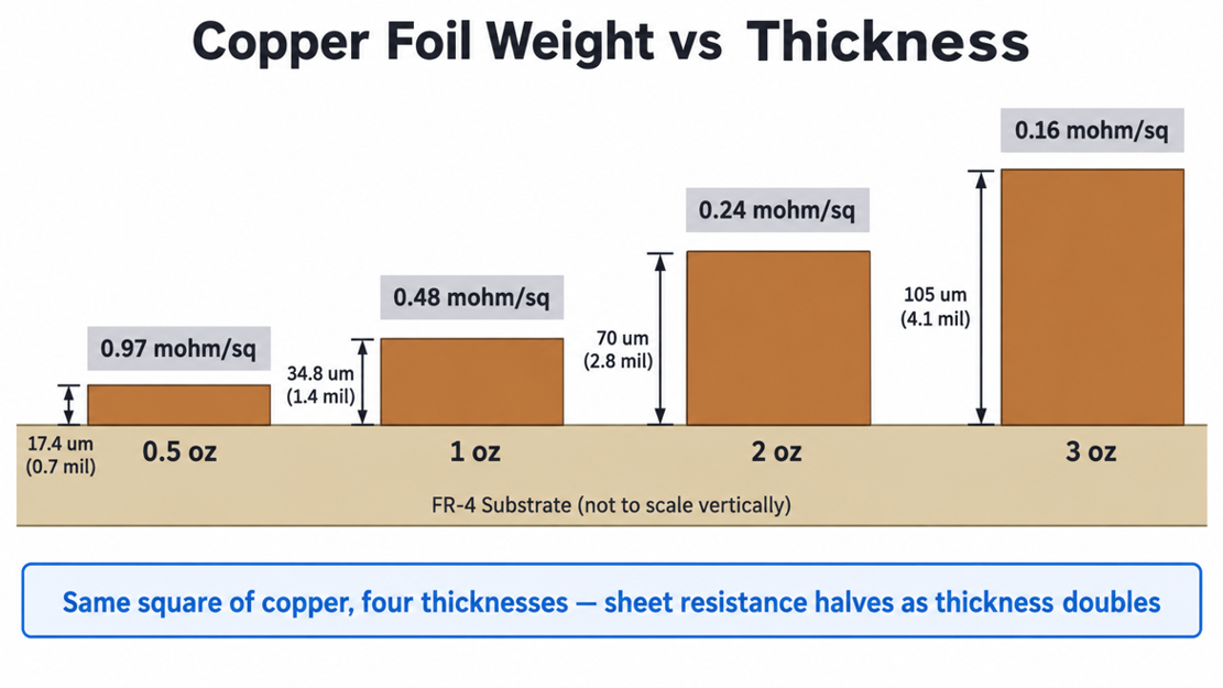
Figure 2: Scale comparison of 0.5 oz, 1 oz, 2 oz, and 3 oz copper foil thickness
| Copper Weight (oz/ft²) | Nominal Thickness | Sheet Resistance (mΩ per square) | Where It Belongs |
|---|---|---|---|
| 0.5 oz | 17.4 µm (0.7 mil) | 0.97 | Inner signal layers are the default on multilayer boards |
| 1 oz | 34.8 µm (1.4 mil) | 0.48 | Default outer copper, general digital and analog work |
| 2 oz | 70 µm (2.8 mil) | 0.24 | Power rails, motor drives, anything past about 3 A |
| 3 oz | 105 µm (4.1 mil) | 0.16 | Entry point for heavy copper and busbar-style planes |
| 4 oz and above | 140 µm (5.5 mil) and above | 0.12 and below | Welding gear, battery packs, high-current backplanes |
The sheet resistance for 1 oz copper is approximately 0.48 mΩ per square. A “square” is a length of copper that is equal to the width, and counting the squares can provide a quick estimation of the trace resistance without having to use a formula.
Understanding Copper Foil in PCB Applications
The manufacturing process transforms a sheet of copper foil into a finished copper circuit layer, and during the process, the thickness and shape of the foil will be modified several times. It is easy to see why an etched trace is not always exactly the size that was drawn in the layout after this process.
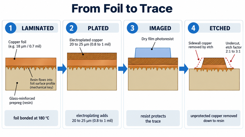
Figure 3: Cross-section showing copper foil laminated, plated, and etched
How Copper Foil Becomes a PCB Circuit Layer
Each of the outer layers changes the copper in a significant way you should know about, as there are five of them:
- Lamination: Foil and prepreg are pressed at roughly 180 C under several hundred psi, so molten resin flows into the foil's rough underside and locks it in place.
- Drilling and hole activation: Holes are drilled through the panel, then a thin electroless copper seed is deposited so the bare resin walls will accept electroplating.
- Imaging: Dry film photoresist is laminated on, exposed through your artwork, and developed, leaving protection only where copper must remain.
- Plating: Electrolytic copper builds the hole barrels and thickens the exposed outer copper simultaneously, typically adding 20 to 25 µm (0.8 to 1 mil).
- Etching and stripping: A cupric chloride or alkaline spray dissolves every unprotected area down to the resin, and the resist is then stripped away.
When etching dissolves copper downwards, it also dissolves the trace sideways. The edges of the finished trace will be slightly trapezoidal with a narrower top as the chemistry eats the foil away.
Standard and Heavy Copper Applications
One ounce of copper covers the overwhelming majority of work, so it is the default outer weight on almost every quick-turn order. It etches down to 0.09 mm features, handles logic and small analog rails comfortably, and costs nothing extra. Current capacity is where it runs out. On a 1 oz outer copper, a trace roughly 0.25 mm (10 mil) wide carries about 1 A.
That figure assumes a 10 C temperature rise and the conservative IPC-2221 charts. IPC-2152 allows more, since it accounts for how the board itself conducts heat, but the older figure keeps you safe. Doubling to 2 oz doubles the cross-section, so the same trace width carries close to twice the current at the same temperature rise. Heavy copper proper begins at 3 oz (105 µm, 4.1 mil), and heavy copper PCB design runs well beyond that for busbar work.
Main Types of Copper Foil Used for PCBs
Two manufacturing routes produce almost all PCB copper foil, but they leave the metal with completely different grain structures.
Electrolytic and Rolled Copper Foil
Electrodeposited foil, commonly called ED foil, is plated from a copper sulfate bath onto a slowly rotating titanium drum. As electrodeposited copper grows on the rotating drum, the crystal structure develops outward from the drum surface. This gives the finished foil two distinct sides: a smooth, shiny drum side and a rougher matte side where the copper growth develops.
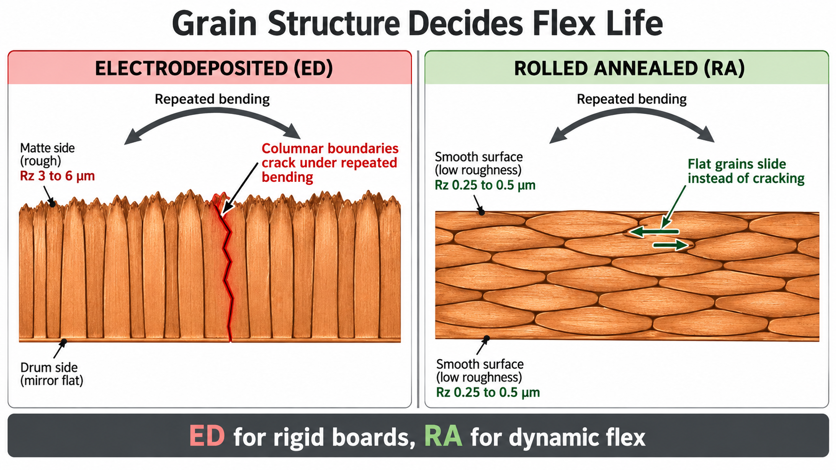
Figure 4: Grain structure comparison of ED and RA copper
Rolled annealed foil (RA foil) begins with a cast copper ingot. Rolled copper is rolled through mills that reduce it to the desired thickness, stretching and flattening the grains so they are approximately parallel to the surface of the foil. Those grains are then allowed to grow and recrystallize by annealing the foil. The outcome is a smooth, double-sided rolled-annealed (RA) copper foil that is much more ductile than electrodeposited foil.
| Foil Type | How It Is Made | Typical Rz Roughness | Where It Earns Its Place |
|---|---|---|---|
| Standard ED | Plated onto a rotating titanium drum | 3 to 6 µm (118 to 236 µin) | Every day, rigid boards operate below about 1 GHz |
| HTE ED (IPC-4562 Grade 3) | ED foil tuned for elongation when hot | 2 to 4 µm (79 to 157 µin) | Multilayer stacks facing repeated lamination cycles |
| Reverse treated (RTF) | ED foil bonded on the smooth drum side | 1 to 1.5 µm (39 to 59 µin) | 5 to 10 GHz digital, the cheapest loss improvement |
| VLP and HVLP | ED foil has grown to a very low profile | 0.3 to 1 µm (12 to 39 µin) | 10 GHz and up, RF laminates, 25 Gbps serial links |
| Rolled annealed (RA) | Cast ingot cold rolled, then annealed | 0.25 to 0.5 µm (10 to 20 µin) | Dynamic flex circuits and low-loss RF |
How to Choose Copper Foil for Different PCB Requirements
Foil choice follows the application, and four cases cover nearly everything you are likely to build:
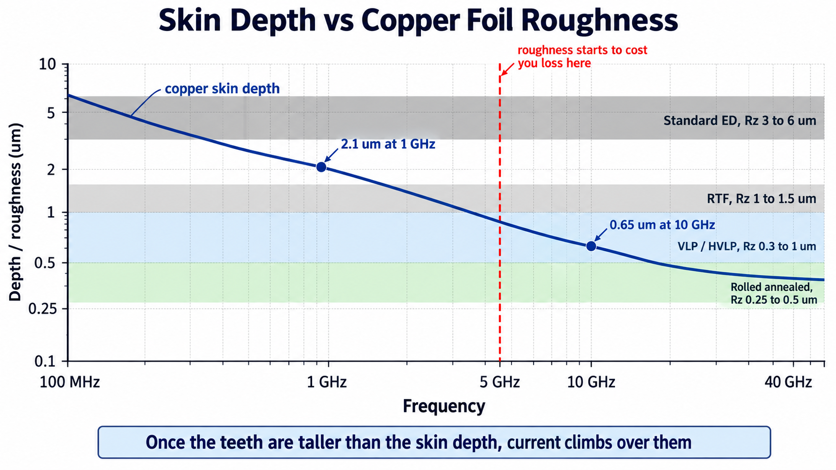
Figure 5: Skin depth versus frequency plotted against typical copper foil roughness
- Rigid digital and analog below roughly 1 GHz: Standard or HTE ED foil, because surface roughness is far smaller than the conducting depth at those frequencies.
- Multilayer boards with three or more lamination cycles: HTE foil specifically, since ordinary ED foil can crack when stretched while hot.
- Flex circuits that bend in service: Rolled annealed foil, as its flat grain structure survives repeated folding, where columnar grains split.
- Links above about 5 GHz or 10 Gbps: Reverse treated, VLP or HVLP foil, since smoother copper directly lowers conductor loss.
Roughness is only a factor when the metal is no longer fully utilized in the current. High-frequency currents have a tendency to “skin,” meaning that they flow near the surface, and the depth at which they do is known as the skin depth. For copper, it is approximately 2.1 µm at 1 GHz and decreases with the square root of frequency.
Copper Foil Uses and Properties That Affect PCB Performance
Copper’s three attributes make it a contender: it conducts electricity, it conducts heat, and it etches cleanly enough to produce fine features.
Electrical, Thermal, and Current-Carrying Properties
The industry refers to the conductivity of copper as 100% IACS, which is 5.8 × 10⁷ S/m. Only silver beats it, and silver just isn’t a cost-effective material to laminate over panels in square meters. The conductivity of aluminum is about 61% that of copper; therefore, an aluminum conductor must be significantly wider to function in the same manner. Copper has a thermal conductivity of approximately 385 W/mK, and the FR-4 material below it has approximately 0.3 W/mK.
Current scales in proportion to copper weight; so does heat. The hot-spot temperature decreases measurably when a 2 oz ground pour is made under a regulator, compared to a 1 oz pour, as the heat transfer through the ground is about doubled. Thermal vias then transfer that heat to the copper on the other side. When sizing a trace for current, it is not a fusing question; it is a temperature question. The trace will heat up and increase in resistance, causing nearby components to fall out of tolerance without any copper melting at any sensible current.
Mechanical Properties, Surface Quality, and Adhesion
Adhesion is measured as peel strength, which is the force required to pull a strip of foil off the laminate. Copper does not chemically bond with cured epoxy, so the grip must be mechanical. It comes from the foil's treated matte side, where fine dendritic teeth are grown and then coated with a zinc or nickel barrier.
Smoothing foil for high-frequency work removes exactly those teeth, so peel strength falls as roughness falls. Foil makers respond with bonding chemistries that replace texture, which is a major reason VLP laminates cost more. Surface defects in the incoming foil survive the entire process. A pit, a dent, or a wrinkle sits quietly under the photoresist. The etchant finds it anyway, so it becomes a nick in a trace or an open circuit.
Copper Foil Selection and PCB Manufacturing Requirements
Copper weight is not a free choice because it depends on layer count, minimum feature size, and how a fab presses your stack-up.
Matching Copper Foil With Layer Count, Stack-Up, and DFM Requirements
Heavier copper requires wider traces and larger clearances because the etchant must cut through more metal. As it etches downward, it also keeps attacking the trace edges, increasing the amount of undercut. JLCPCB publishes the minimum trace width and spacing for each copper weight, so the routing trade-off can be checked before layout begins.
| Finished Copper Weight | Board Types Offered | Minimum Trace / Space | What It Costs You in Density |
|---|---|---|---|
| 1 oz (34.8 µm, 1.4 mil) | 1 to 2-layer and 4+ layer outer | 0.09 to 0.10 mm (3.5 to 4 mil) | None, fine-pitch BGA fanout still works |
| 2 oz (70 µm, 2.8 mil) | 1 to 2-layer and 4+ layer outer | 0.15 to 0.16 mm (6 to 6.5 mil) | Roughly 60% wider minimum feature |
| 2.5 oz (87 µm, 3.4 mil) | 1 to 2-layer only | 0.20 mm (8 mil) | Fine-pitch escape routing is gone |
| 3.5 oz (122 µm, 4.8 mil) | 1 to 2-layer only | 0.25 mm (10 mil) | Power layout only, no dense signals |
| 4.5 oz (157 µm, 6.2 mil) | 1 to 2-layer only | 0.30 mm (12 mil) | Busbar-style pours with a handful of nets |
Outer copper on 4-layer and higher boards is offered in 1 oz or 2 oz only. A 2-layer board, by contrast, can go to 4.5 oz (157 µm, 6.2 mil). Inner layers run 0.5 oz, 1 oz, or 2 oz, and 0.5 oz is what you get unless you ask for more.
Maintaining Copper Thickness and Manufacturing Consistency
The ordered copper weight and finished copper weight are different numbers on the outer layers. Fabs commonly start with 0.5 oz foil and electroplate it up, because the same plating bath has to fill the through-holes anyway. A board sold as 1 oz outer therefore arrives as foil plus plating that together meet the finished specification. Outer copper consequently varies more than inner copper.
Plating current density is never uniform across a panel, so boards near the edges can collect slightly more copper than those in the middle. Trace width carries its own tolerance, published by JLCPCB as ±20%. A drawn 0.2 mm (8 mil) trace can legitimately fall anywhere between 0.16 mm (6.3 mil) and 0.24 mm (9.4 mil). Size marginal power traces against the low end, so the worst acceptable board still meets your temperature target.
How PCB Manufacturers Control Copper Foil Quality
Copper foil arrives certified, yet a fab still has to prove it survived lamination, etching, and plating unchanged. Quality control for copper is a chain of checks running from goods-in to a polished microsection.
Material Inspection, Etching, and Plating Control
Thickness, weight, peel strength, and profile class all appear on that document, and the foil then sits in a humidity-controlled store. Oxidized foil bonds poorly, so storage is genuine process control rather than housekeeping. The etch line decides the finished trace width, so it gets the tightest control of any wet process. Cupric chloride baths are held to a specific gravity, a redox potential, and a temperature window. Conveyor speed is then trimmed to hold the etch rate steady.
JLCPCB lists 1 oz through 4.5 oz outer copper on 2-layer boards, and 1 oz or 2 oz on multilayer boards. It also publishes the exact minimum trace and space tied to each weight. You can upload your Gerbers and quote with the copper weight already selected. The automatic DFM check then flags any feature that the weight cannot hold.
AOI, Cross-Section Analysis, and Reliability Testing
Automated optical inspection takes photographs of each etched layer and compares them to CAM data. It snaps, nicks, mouse bites, shorts, and copper that etched out where it should have remained. Inner layers are checked prior to lamination, as once laminated, a fault can never be fixed.
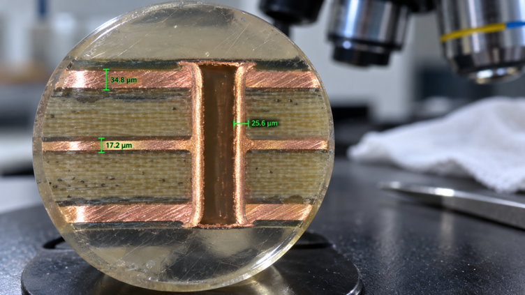
Figure 6: PCB under a metallurgical microscope showing measured copper thickness
The thickness can only be checked by cutting the board open and physically checking the thickness. A coupon is set in epoxy, polished back, and then viewed under a microscope. That provides a direct measurement of foil thickness, plated copper, and etch factor. Thermal stress testing addresses the question of whether the foil is actually bonded or not. A sample is floated on molten solder at 288 °C for 10 seconds and microsectioned for lifted-foil or resin separation. Peel strength testing gives the same answer as a number, rather than a photograph.
FAQ About Copper Foil in PCBs
Q: How thick is 1 oz copper foil in microns and mils?
One ounce of copper spread over one square foot gives a nominal thickness of 34.8 µm, or 1.37 mil. The industry usually rounds that figure to 35 µm. Half-ounce copper is 17.4 µm (0.7 mil), and 2 oz copper is 70 µm (2.8 mil).
Q: Do inner layers get the same copper weight as outer layers?
No, and assuming they do is a common source of undersized power planes. Multilayer boards default to 0.5 oz inner copper, with 1 oz and 2 oz available on request. Inner layers are never electroplated either, so they finish at exactly the foil weight ordered.
Q:What is the real difference between ED and rolled annealed copper foil?
Electrodeposited foil is plated onto a drum, giving vertical columnar grains that crack when repeatedly bent. Rolled annealed foil is cold-rolled and annealed, producing flat, overlapping grains that slide rather than crack.
Q: At what frequency does copper foil roughness start to matter?
Roughness becomes significant once the skin depth approaches the height of the surface teeth, which happens around 5 GHz for standard foil. Copper skin depth is about 2.1 µm at 1 GHz and roughly 0.65 µm at 10 GHz.
Q:Why is my finished outer copper thicker than the foil weight I ordered?
Outer layers are electroplated during through-hole plating, which adds roughly 20 to 25 µm on top of the starting foil. Fabs usually begin with thinner foil and plate up to reach the finished weight.
Conclusion
Copper foil is the one material in a PCB that you specify with a single number and then live with everywhere. That number sets resistance and current capacity, and it sets how well a plane spreads heat. Through the etch factor, it also decides how fine your traces are allowed to be. Foil type adds a second axis, deciding whether the board can flex and how much a fast edge loses crossing it. Treat the copper decision as part of the stack-up rather than as a checkbox at checkout.
Pick the weight from the current weight your rails actually carry, and keep it symmetric so the panel presses flat. Reach for smoother foil only when your edge rates justify the peel strength you give up. Data rates keep climbing, so foil roughness will start mattering on ordinary digital boards sooner than most designers expect. Published capability tables and an automatic DFM check make it cheap to test before a panel is committed.

Keep Learning
Safeguarding Circuit Boards Against Breakdown Voltage Failure
Key Takeaways Construction Matters: Breakdown voltage depends on stackup and defects, not raw material ratings. Stress Causes Failures: Heat and moisture degrade insulation over time, leading to field defects. Four Main Failure Modes: Insulation fails via internal voids, treeing, CAF growth, or surface tracking. Layout Design Fixes: Use dual prepregs, wider hole spacing, rounded trace corners, and isolation slots. Testing Split: Bare-board testing checks low-voltage net continuity, while hi-pot tests ......
Is FR4 the Best Board Material for Your Design
Key Takeaways Best All-Rounder: Ideal balance of strength, insulation, and low cost for standard PCBs. Clear Limits: Poor heat dissipation (~0.3 W/m·K) and high loss for RF (>3 GHz). Alternatives: Use Rogers for RF, Aluminum for high heat, and FPC for flexibility. Selection Essentials: Pick High-Tg (170°C+) for lead-free reflow and custom stackups for impedance. JLCPCB Advantage: 1–32 layer FR4 boards with ±10% impedance control and 24h fast dispatch. In the world of electronics and printed circuit bo......
Optimizing High-Voltage Circuit Safety with PCB Dielectric Strength
Key Takeaways Non-linear Scaling: Dielectric strength drops as thickness increases. Safety vs Signals: Dielectric strength ensures safety, while Dk controls signal speed. Material Selection: High-voltage safety depends on Tg, CTI, and moisture resistance. Spacing Rules: Clearance prevents air arcs, while creepage prevents surface tracking. Assembly Testing: Hi-pot testing requires finished assemblies, not bare boards. Dielectric strength is the number engineers quote to prove a board is safe at mains ......
How Copper Foil Shapes PCB Performance and Manufacturing Quality
Key Takeaways Weight: 1 oz copper ≈ 35 µm thickness; higher weight increases current capacity. Types: ED for standard rigid boards, RA for dynamic flex circuits. DFM & Loss: Smoother foil lowers RF loss; thicker foil requires wider trace spacing. The part of a PCB that actually carries the electrical signal is the copper foil. The strength comes from the glass weave, the resin is used to keep the layers together, and the solder mask is used to provide protection and separation of exposed copper. But w......
Why PCB Substrate Choice Matters More Than You Think
Key Takeaways Prevents Via Failures: Z-axis CTE expansion strains via barrels; right substrates prevent field failure. Specify Beyond FR-4: Name IPC-4101 sheets to guarantee proper Tg and lower thermal growth. Match Material to Need: Choose FR-4 for standard, Polyimide for flex, Aluminum for heat, and Rogers for >3 GHz. Use Real Fab Stackups: Prepreg weave alters Dk; compute impedance using real factory stackups. The PCB substrate is the one part of your board you never actually draw. You choose a thi......
A Complete Guide to Copper Clad Laminate (CCL) in PCB Manufacturing
Key Takeaways CCL is the base material: a cured resin-reinforcement sheet with copper foil bonded to one or both sides. Three parts control performance: Resin affects heat and loss, reinforcement controls stability, and copper foil affects conductor behavior. Choose by the main design stress: Heat, frequency, and cost usually determine the best laminate family. Slash sheets define the material: IPC-4101 uses numbered slash sheets to specify rigid PCB base materials. Tg alone is not enough: Td and time......