Buried Vias in Advanced PCBs: Enabling Higher Density, Better Signal Integrity, and Compact Designs
16 min
- Understanding Buried Vias and Their Place in PCB Technology
- Structural and Functional Advantages of Buried Vias
- Design Rules and Best Practices for Buried Vias
- Buried Via Design Requirements for Manufacturing
- Manufacturing Considerations for Reliable Buried Vias
- Real-World Applications and Performance Gains
- FAQ about Buried Vias
- Conclusion:
Key Takeaways
- Hidden Routing: Buried vias connect only inner layers, keeping outer surfaces clear for dense components and traces.
- Better Signal Integrity: They eliminate via stubs, reducing parasitics and signal loss in high-speed designs.
- Higher Density: Essential for HDI boards, dense BGAs, and small form factors like wearables.
- Higher Cost: Sequential lamination and extra drilling steps make them ~3×-4× more expensive than standard through-holes.
Ever wondered how a modern smartphone mainboard can fit thousands of connections on a credit card-sized board? Much of that answer lies in the buried via, an interconnect that resides entirely within the board, out of sight on either surface. It takes the most work and does it quietly, leaving components and fine routing out of the way. A plain through-hole via is sufficient for most of the designs used on a day-to-day basis with 2 layers.
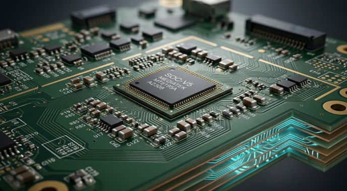
However, the buried via is no longer a luxury and more of a necessity, once you reach high-density interconnect (HDI) levels, dense BGAs, high-speed buses, and tight form factors. It alters the way you view layer count, routing channels, and signal integrity - all at once. In this guide, we will go through the definition, differences between buried, blind, and through-hole vias, design guidelines that should be followed, and the manufacturing process of sequential lamination. At the end, you will be able to select the right times to use buried vias and what they will cost you in complexity.
Understanding Buried Vias and Their Place in PCB Technology
However, it's important to first understand the physical location of a via type well in the stackup before it is possible to use it. That's where much of the confusion between blind and buried vias begins.
Definition and Comparison with Through-Hole and Blind Vias
Buried via is a plated hole that does not make contact with either of the outside layers of a multilayer PCB, but connects to two or more inner layers of copper. Truly hidden by the outer layers, it won't be visible when the board is laminated, which is why it's called "buried.
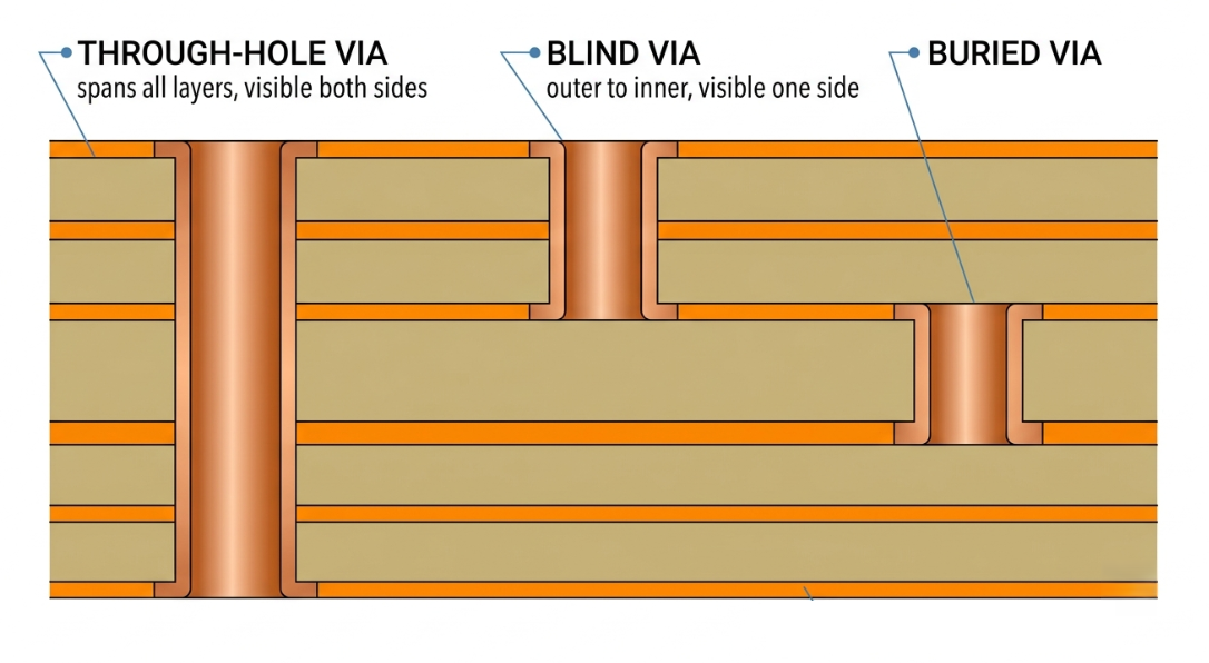
Compare with the other two typical structures. A through-hole via penetrates the entire board from top to bottom, and is the easiest and most economical to create. Blind via is a via that only appears from one side and does not appear on the other side.
The table below is an overview of the practical differences to consider during the design.
| Via Type | Layer Span | Visible From Surface | Drilling Stage | Typical Size | Relative Cost | Best Use |
|---|---|---|---|---|---|---|
| Through-hole via | Top to bottom (all layers) | Both sides | After full lamination | 0.2–0.3 mm | Lowest (1x) | Standard 2–8 layer boards, power/ground |
| Blind via | Outer layer to an inner layer | One side only | On outer sub-core / laser | 0.1–0.15 mm | Higher (2–3x) | Surface BGA fan-out, HDI outer transitions |
| Buried via | Inner layer to inner layer | Neither side | On the inner sub-core before the final press | 0.15 mm or larger | Highest (3–4x) | Inner-layer routing, dense HDI cores |
Take away: The hole-type of a through-hole via takes up real estate on each layer it traverses, whereas a buried via hole only passes through layers that it actually connects. This one differentiates and makes it so powerful within the tight designs.
Why Buried Vias Are Essential for Modern High-Density Boards
This is powered by modern components. When you have a large FPGA or SoC in a fine-pitch BGA package, you may have hundreds of balls, and each individual signal must go somewhere. If all of them were to be through-hole vias, then the space would be consumed, and escape routing would be impossible.
Buried vias overcome this by providing the interconnects deep in the board, while the outer layers are used for pads and short fan-out traces. This is why blind and buried vias are the foundation of HDI construction. You are not competing for an increasingly limited amount of 2D space; they allow you to route in 3D. That is why manufacturers like JLCPCB provide these structures as part of their HDI service: because otherwise, there is no way to create such dense, high-pin-count designs.
Structural and Functional Advantages of Buried Vias
There are a number of advantages to the buried via hole, in addition to being able to pack more traces. They have an impact on electrical performance, board size, and even on total layer count.
Space Optimization by Avoiding Outer Layer Interference
The first benefit is to have a home. Since a buried via is never exposed to the surface, it can never interfere with a component pad, solder mask opening, or surface trace on the outer layers. Imagine that the outside layers are prime real estate in the downtown area. Through-holes punched through them are wasted land. A PCB buried via is available for the things that really need to be on the surface.
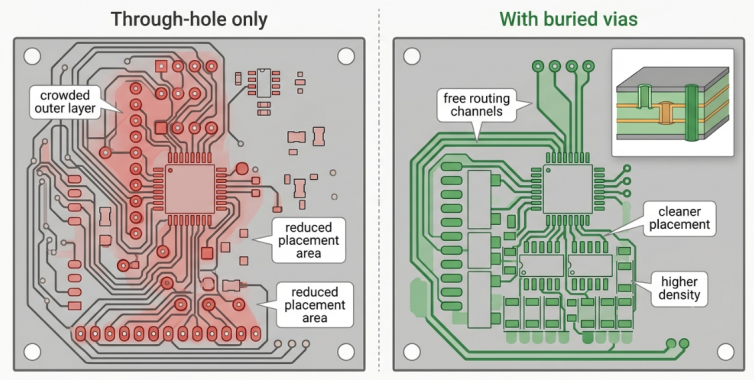
- No extra routing channels for the outer layer for critical high-speed traces.
- Cleaner component placement, without vias interrupting pad arrays.
- More connections in the same size.
- Enhanced fan-out from dense pitch BGAs and QFNs.
Improved Signal Paths and Reduced Parasitic Effects
Buried vias are also electrically helpful. The shorter, more compact interconnect will have less parasitic inductance and capacitance than a complete through-hole barrel that extends through the entire stackup. The "via stub" is the leftover barrel on a through-hole via, and is no secret as a source of reflections and insertion loss at high frequencies.
A buried via that only touches the layers that it needs gets rid of that stub altogether and provides you with a cleaner signal path. This provides improved signal integrity for high-speed nets with less impedance discontinuity, less crosstalk between adjacent layer signals, and better return-path control if the via is near its reference plane.
Support for Reduced Layer Count and Smaller Form Factors
This is one of the perks that many designers don't know about. Sometimes buried vias will allow you to decrease the overall number of layers that a board requires. Once all the interconnects are no longer required to be on every layer, routing freedom is gained that can reduce the number of signal layers to two. Fewer layers translates into a lighter, thinner board and often a lower cost board, although each individual via may be more expensive. In the case of compact IoT modules and wearables, this trade can often be a make-or-break decision for blind and buried vias.
Design Rules and Best Practices for Buried Vias
Buried vias are a blessing for a good plan and a curse for a bad stackup job. But a few disciplined rules will help ensure your design will be manufacturable, and your yield will be high.
Aspect Ratio Limits, Depth Control, and Placement Guidelines
The most critical number is the aspect ratio, which is the ratio of the depth of the via to the diameter of the via that is drilled. The ratio needs to be maintained within your fabricator's range, usually 8:1 to 10:1 in mechanically drilled buried vias to ensure reliable plating.
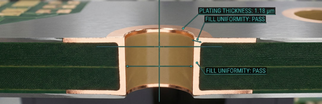
If the via is too deep for the diameter of the via, then the plating solution will not flow freely, and the barrel will plate unevenly, resulting in open circuits and voids. Here are some rules for placement and size:
- Determine the span's diameter: buried via diameters of 0.15 mm (6 mil) or less are commonly used in HDI, but verify the buried via with the number of layers that it is traversing.
- Follow the aspect ratio budget to fully and evenly barrel plate.
- Avoid placing vias on outer-layer SMT pads, as this can cause solder flux to become trapped, a common reliability problem.
- List the vias as groups to the pairs of layers to which they go so that the fabricator can drill them together on a single sub-core.
Integration with Stackup, Impedance, and Via Stacking
A buried via cannot be as good as the stackup it resides in. Each buried via will go between a certain pair of layers, which must be specified in advance, since this will affect the stage of laminating the board. Buried vias typically are drilled across an even number of copper layers, and are located on symmetric sub-cores to maintain the balance of the pressed stack. If a buried via is used for a continuous connection under a blind via, it is usually necessary to have the buried via copper-filled and planarized to have the upper via land on a flat, solid surface. Make sure this does not conflict with your impedance goals. If you have a change of reference planes with a via transition, you can upset a controlled impedance net if you don't take care of the return path.
Coordination with Blind Vias for Sequential Build-Up
Buried and blind vias are used in tandem in advanced HDI. The buried via is used for a deep connection between the inner-layer and the core, while the blind via is used for the connection from the inner-layer to the outer-layer during build-up.
Here is the concept of a Blind Buried via using the PCB stackup method: The inner buried core is first made, then the outer layers containing blind vias are added on top one-by-one. Planning both types of roads at the same time, instead of as an afterthought, makes for a clean, routable, and cost-effective sequential build-up.
Buried Via Design Requirements for Manufacturing
| Design Parameter | JLCPCB HDI Design Consideration |
|---|---|
| Via Diameter | Select the via diameter according to the required layer span and manufacturing process. |
| Aspect Ratio | Mechanical buried vias and through vias should have an aspect ratio of ≤16:1. |
| Layer Span | Define the inner-layer connection clearly when designing buried vias. |
| Stackup | Plan the buried-via structure together with the HDI stackup and lamination sequence. |
| Annular Ring | The annular ring for blind and buried vias should be at least 0.075 mm. |
| Hole-Edge Spacing | Keep the hole-edge spacing between different nets at ≥0.24 mm. |
| Line/Space | The minimum line width/spacing is 3/3 mil; 3.5/3.5 mil is recommended when space allows. |
| Via Filling | For HDI structures, blind and buried vias are filled using different processes according to their structure. |
These parameters should be reviewed together with the PCB manufacturer before layout is finalized. Early DFM review can help identify stackup, drilling, and registration issues before they lead to costly redesigns.
JLCPCB Buried Via HDI Manufacturing Capabilities
JLCPCB's HDI PCB manufacturing supports blind and buried via structures for high-density designs. Its HDI capabilities include laser-drilled microvias, multi-order HDI structures, sequential lamination, and dedicated processes for blind and buried via filling and plating.
| Capability | JLCPCB HDI Capability |
|---|---|
| Blind Via Diameter | 0.075–0.15 mm |
| Default Laser Hole Diameter | 0.1 mm |
| HDI Orders | 1st-, 2nd-, and 3rd-order |
| Buried Via / Through Via Aspect Ratio | ≤16:1 |
| Blind & Buried Via Annular Ring | ≥0.075 mm |
| Hole-Edge Spacing | ≥0.24 mm |
| Minimum Line/Space | 3/3 mil |
| HDI Materials | Shengyi and Nanya |
| Blind Via Filling | Electroplated filling and planarization |
| Buried Via Filling | Resin plugging and plating/capping |
Manufacturing Considerations for Reliable Buried Vias
Knowing how buried vias are fabricated helps you to create boards that can get through the fabrication process without any surprises.
Sequential Lamination and Precision Drilling Techniques
Buried vias involve sequential lamination, unlike a simple board, which is laminated once and then drilled. First, the inner core is processed as an independent thin board and afterward bonded in the stack.
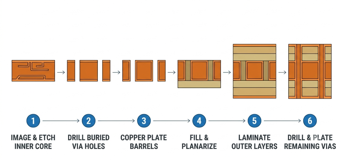
The flow should be approximately as follows:
- Etch and image the inner-layer core on which the buried vias will be desired.
- Make accurate and controlled depth or through-core drilling of the buried via holes in that core.
- Plating the buried via barrels with copper to create the electrical connection.
- If a via-on-via stack will be placed on top, fill and planarize vias.
- Apply laminate and prepreg on top of the completed core.
- Drill and plate the rest of the through hole or blind vias on the built-up stack.
The buried via is drilled before the outer layers are even present, so inter-layer registration is key, and the outer layers have to line up with holes that they can't see.
Plating, Filling, and Inspection Challenges
Once a buried via is plated, it cannot be reworked and is unforgiving. Voids, thin areas, and trapped voids within the barrel are permanently closed when the outer layers are pressed on. Fabricators fill or plug the plated barrel with conductive or non-conductive epoxy or with electroplated copper, and cap it flat, to eliminate internal voids. It's also difficult to inspect – quality control relies on cross-section coupons and X-ray to test that the plating is thick and well filled in the representative sample, not the actual production hole.
Cost and Complexity Factors in HDI Fabrication
Each additional lamination cycle increases costs, time, and yield risk. Buried vias require a minimum of one extra press, drill, and plate process compared to the standard multilayer board; that's why they're at the top of the cost table.
A buried via design will cost about 3-4 times the fabrication cost of a board of the same size, but only with through-hole design, due to additional tooling, tighter registration tolerances, and increased inspection. That's where a manufacturer's DFM review comes in handy. If you go through a service such as JLCPCB's HDI DFM check early, you'll be able to find out if your aspect ratio or layer-span is unmanufacturable before it gets to be an expensive respin.
Real-World Applications and Performance Gains
Therefore, buried vias are where? Wherever density, speed, or size requirements exceed those of through-hole construction.
High-Speed Computing and Telecommunications Equipment
Multi-gigabit buses drive servers, network switches, and 5G radio units, in which stubs and long barrels are the enemy. Buried vias provide a clean, short connection in the inner-layer of the board to maintain eye margins on DDR, PCIe, and high-speed SerDes connections. In these systems, the use of blind and buried vias can facilitate the huge number of pins found in today's processors and switch fabrics and maintain insertion loss levels. This performance improvement is seen directly as a higher data rate achievable and higher reliability.
Medical and Aerospace Devices Requiring Reliability
When designing implantable medical electronics and avionics for aerospace applications, size and reliability are critical. A buried via is a strong, mechanically protected interconnect protected by the surrounding layers when it is properly plated and filled
- Tiny medical devices that don't have a lot of spare room.
- Avionics and satellite modules for vibration and thermal cycling.
- High-reliability up to IPC Class 3, cross-section verification by integrity.
The via is buried, which offers a subtle but useful reliability benefit by protecting the via from surface stresses and handling damage.
Consumer Wearables and Compact IoT Modules
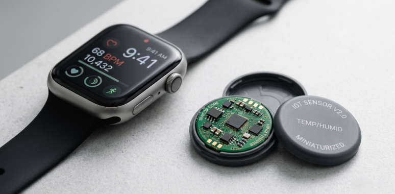
Buried vias are most noticeable in smartwatches, hearables, fitness bands, and tiny IoT sensors. These products require the smallest possible board and the highest possible function density. A PCB buried via is a vertical interconnect for a PCB designed by a designer that could be 10 layers of through-hole routing, but is converted to a four- or six-layer HDI board. That means smaller batteries, smaller enclosures, and lighter weight, the things consumers care about. The small stackups are available for the makers who want to take a wearable prototype to production, which is supported by HDI services with buried and blind via support.
FAQ about Buried Vias
Q: What is the difference between a blind via and a buried via?
A blind via connects an outer layer to an inner layer, so it is visible from one surface of the board. A buried via connects only inner layers and cannot be seen from either surface, since it is fully enclosed by the outer layers.
Q: Why do buried vias cost more than through-hole vias?
Buried vias require sequential lamination, meaning the inner core is drilled and plated as a separate step before the outer layers are pressed on. These extra press, drill, and plating cycles add tooling, time, and yield risk, typically raising fabrication cost to roughly 3–4x that of a through-hole-only board.
Q: Can buried vias improve signal integrity?
Yes. Because a buried via spans only the inner layers it connects, it avoids the long unused barrel, or via stub, of a full through-hole via. This reduces parasitic inductance, capacitance, and reflections, which helps preserve clean high-speed signals.
Q: What aspect ratio should I use for buried vias?
Most fabricators support mechanically drilled buried vias up to around an 8:1 to 10:1 depth-to-diameter aspect ratio. Staying within this limit ensures the barrel plates are evenly spaced and avoid voids; always confirm the exact value with your manufacturer's capability sheet.
Q: Where can I get PCBs with buried vias manufactured?
Buried vias are a standard part of high-density interconnect (HDI) fabrication, so any capable HDI manufacturer can build them. JLCPCB offers HDI PCB services with blind and buried via support, an instant quoting system, and a DFM review that flags aspect ratio or stackup issues before production.
Conclusion:
Today, buried via is much more than just hidden via to achieve compact layout, improve signal integrity, and increase routing density in modern HDI PCB design. They provide surface area saving by only connecting necessary inner layers, reducing unnecessary via stubs, and satisfy the high-speed requirements of computing, telecommunications, aerospace, medical electronics, and wearable devices.
While the fabrication complexity and cost of buried vias (due to sequential lamination) may be a disadvantage in certain designs, these are often outweighed by the performance and space-saving benefits of buried vias, especially in advanced designs. Knowing about buried via PCB technology, using proven design rules, and working with a good manufacturer will help you to design reliable, manufacturable multilayer boards that meet the performance requirements of today's next-generation electronic products.

Keep Learning
How Copper Foil Shapes PCB Performance and Manufacturing Quality
Key Takeaways Weight: 1 oz copper ≈ 35 µm thickness; higher weight increases current capacity. Types: ED for standard rigid boards, RA for dynamic flex circuits. DFM & Loss: Smoother foil lowers RF loss; thicker foil requires wider trace spacing. The part of a PCB that actually carries the electrical signal is the copper foil. The strength comes from the glass weave, the resin is used to keep the layers together, and the solder mask is used to provide protection and separation of exposed copper. But w......
A Complete Guide to Copper Clad Laminate (CCL) in PCB Manufacturing
Key Takeaways CCL is the base material: a cured resin-reinforcement sheet with copper foil bonded to one or both sides. Three parts control performance: Resin affects heat and loss, reinforcement controls stability, and copper foil affects conductor behavior. Choose by the main design stress: Heat, frequency, and cost usually determine the best laminate family. Slash sheets define the material: IPC-4101 uses numbered slash sheets to specify rigid PCB base materials. Tg alone is not enough: Td and time......
Buried Vias in Advanced PCBs: Enabling Higher Density, Better Signal Integrity, and Compact Designs
Key Takeaways Hidden Routing: Buried vias connect only inner layers, keeping outer surfaces clear for dense components and traces. Better Signal Integrity: They eliminate via stubs, reducing parasitics and signal loss in high-speed designs. Higher Density: Essential for HDI boards, dense BGAs, and small form factors like wearables. Higher Cost: Sequential lamination and extra drilling steps make them ~3×-4× more expensive than standard through-holes. Ever wondered how a modern smartphone mainboard can......
Unlocking Higher Density and Better Performance with Blind Vias in HDI PCBs
Key Takeaway Higher Density: Connects surface to inner layers without penetrating the whole board, freeing routing channels under fine-pitch BGAs. Improved Signal Integrity: Reduces via stub length to minimize impedance discontinuities in high-speed designs. Aspect Ratio Rule: Keep the depth-to-diameter ratio near 0.75:1 (max 1:1) for reliable laser drilling and void-free plating. Thermal Efficiency: Supports via-in-pad setups for better heat dissipation and compact component placement. Ever wonder ho......
How to Select Tg of PCB ?
What is the Tg of PCB? In PCB manufacturing, "Tg" stands for Glass Transition Temperature. It is the temperature at which the PCB substrate material transitions from a rigid, glassy state to a soft, rubbery state. PCBs are flame-retardant (UL94 V-0) and do not burn easily; instead, they soften above Tg. The Critical Correlation Between Tg and Z-Axis CTE (Coefficient of Thermal Expansion) When the temperature exceeds the Tg point, the PCB substrate material (such as standard FR-4) undergoes a physical ......
Beyond the Basics: The Role of PTFE PCBs
Polytetrafluoroethylene (PTFE) PCBs are integral to advanced electronic applications. Among various PCB materials, Teflon, the brand name for Polytetrafluoroethylene (PTFE). Teflon PCBs, known for their high frequency and heat resistance properties. All of this is achievable due to its exceptional dielectric properties. RF PCB designs often make use of low-loss PTFE-based materials thanks to their very low dielectric losses and huge range of possible Dk values. Low Dielectric Constant: Enables high-sp......