Unlocking Higher Density and Better Performance with Blind Vias in HDI PCBs
14 min
- What Blind Vias Are and How They Work
- Major Benefits of Using Blind Vias
- Design Considerations for Successful Blind Via Implementation
- Blind Via Design Requirements for HDI Manufacturing
- Manufacturing Challenges and Advanced Solutions
- JLCPCB's Expertise in Blind Via HDI PCB Production
- Frequently Asked Questions (FAQ)
- Conclusion
Key Takeaway
- Higher Density: Connects surface to inner layers without penetrating the whole board, freeing routing channels under fine-pitch BGAs.
- Improved Signal Integrity: Reduces via stub length to minimize impedance discontinuities in high-speed designs.
- Aspect Ratio Rule: Keep the depth-to-diameter ratio near 0.75:1 (max 1:1) for reliable laser drilling and void-free plating.
- Thermal Efficiency: Supports via-in-pad setups for better heat dissipation and compact component placement.
Ever wonder how all of those high-speed signals get out of a 0.4 mm pitch BGA without a rat's nest of traces on the tiny board inside a modern smartphone? It's usually the blind via. It's a silent workhorse of high-density interconnect design, and is key to today's small, high-speed electronics. With continuing miniaturization of components and increasing signal speeds, it's just a hole in a board. This is the place where blind vias, in addition to their cousin (buried vias), turn the game inside an HDI PCB.
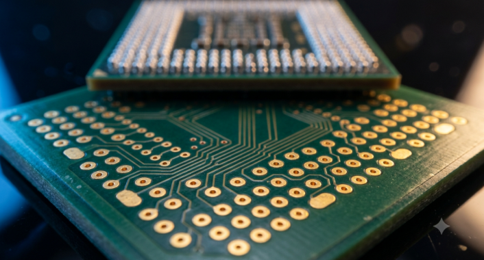
They save routing channels, reduce signal length, and allow you to reduce the size of the board without compromising connectivity. Let's dip our toes in the water and explore what a PCB blind via is, the differences between it and through and buried vias, and its importance to density and performance. Design rules and manufacturing controls that differentiate between a reliable blind via and a field failure will also be addressed. Let's dig in.
What Blind Vias Are and How They Work
A via is just a plated hole to pass a signal/power from one copper layer to another. The differences between the two types of via are the layers that they are crossing and the distance they are penetrating the stackup.
Definition of Blind Vias and Comparison with Through Vias and Buried Vias
A blind via is a via that runs from the outside to an inner layer of the board but does not completely penetrate the board. It appears, on the outside, to be just a hole that ends somewhere, and hence the name “blind”. It will only use the layers that it requires and leave the rest of the layers untouched during the termination process, as it terminates inside the stackup.
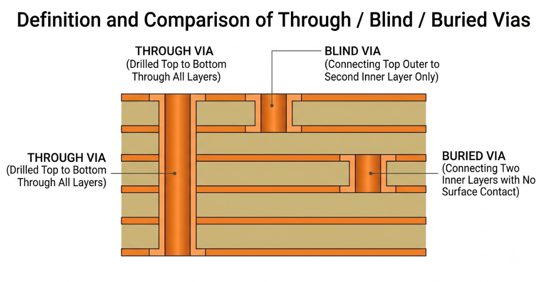
That's as compared to a through via that is physically drilled from top to bottom, and bridges all layers through which it passes. A buried via is completely covered inside the board and does not connect to the top or bottom surface. Blind and buried vias enable designers to route much more densely than they could on a through-only board.
The three are compared side-by-side:
| Feature | Through Via | Blind Via | Buried Via |
|---|---|---|---|
| Layer span | Top layer to bottom layer (all layers) | Outer layer to inner layer(s) only | Inner layer to inner layer only |
| Drilling method | Mechanical drill | Laser (microvia) or controlled-depth drill | Laser/mechanical, drilled before lamination |
| Typical finished size | 0.2–0.3 mm and up | 0.1–0.15 mm (laser microvia) | 0.15–0.3 mm |
| Relative cost | Lowest | Higher | Highest (needs sequential lamination) |
| Typical use case | Standard multilayer, through-hole parts | BGA fanout, surface-to-inner escape routing | Dense inner-layer routing in HDI cores |
The Role of Blind Vias in HDI PCB Architecture
Microvias, fine lines, and thin dielectrics are the defining characteristics of HDI PCBs. The main method for routing signals from a densely populated surface component to the routing layers under it is via blind vias, typically laser-created microvias. The majority of HDI boards can be defined by the buildup of the board, for example, 1+N+1, 2+N+2, etc. A 1+N+1 board is one with a layer of buildup on both sides of an ordinary N-layer core board, and a 2+N+2 board has an additional layer of buildup on each side.
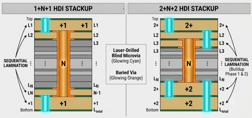
They are both blind microvias that make the transition from the outer to the inner and buried vias that make the connection within the core. Blind vias allow the interconnect to be staged one layer at a time, as each buildup layer is laminated sequentially. This is why it is possible to fan-out a fine-pitch BGA, which is impossible with a single through-drilled board.
Major Benefits of Using Blind Vias
Then what's the point of putting in the extra effort? The blind not only addresses the area of space constraint, but also speed and reliability.
Increased Routing Density and Smaller Board Size
Obviously, density is the first advantage. A thorough via blocks routing on every layer they cross due to copper being used all the way down in the barrel and antipads, even when it is not used on the layer it is routing through. A blind via that connects to the top layers only is not used in the layers below it. Under a dense BGA, the space recovered quickly is enormous, as you can drop signals directly into the buildup layers and route them out under the part.
- If routing channels need to be more usable, they are now more per layer.
- Better BGA escape and fan-out performance with fine pitch parts.
- Less overall board space for the same number of nets!
Improved Signal Integrity and Reduced Layer Count
Shorter vias lead to shorter stubs. A blind via through two or three layers will have a much lower amount of free barrel than a via through a thick board, and so will have a smaller via stub, and less impedance discontinuity to high-speed signals. This is important for multi-gigabit interfaces such as DDR, PCIe, and serial links, where the stub resonances spoil the eye. There's a lesser advantage as well. Blind vias also provide the benefit of conserving routing space, allowing you to achieve the same results as a through-only design with fewer layers, which will help cover up some of the extra expense incurred by creating an HDI.
Better Thermal and Mechanical Performance
Many HDI processes are deep and shallow blind microvia with copper being the filling material, providing good mechanical strength. The filled and capped blind via can even be placed directly in a pad (via-in-pad), which can pass heat and current directly into the copper underneath. This reduces current paths and current handling in close power wiring systems. It also eliminates an open hole-in-pad that would otherwise attract solder during the assembly process.
Design Considerations for Successful Blind Via Implementation
Aspect Ratio, Depth Control, and Via Positioning Rules
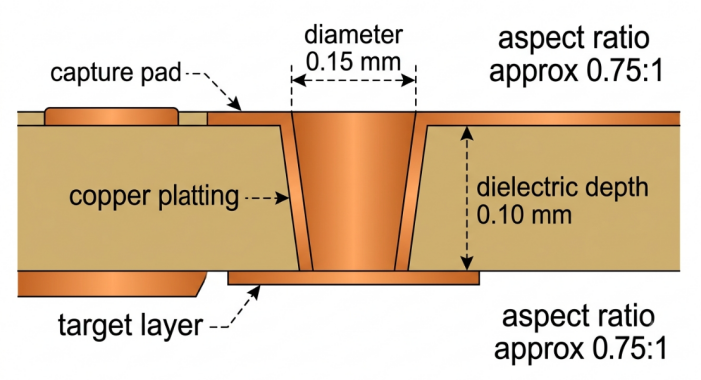
The single most important parameter is aspect ratio, the ratio of via depth to via diameter. The plating chemistry must reach the bottom of the hole, which is only possible for laser-drilled blind microvias when this ratio remains low. Generally, aim for a microvia aspect ratio of around 0.75:1, and 1:1 is a safe maximum.
It is approximately 0.67:1 (numbers) after a laser of 0.15 mm and a dielectric of 0.1 mm (laser plate cleaned), which is also suitable for plates of 0.17 mm. If the dielectric is pushed thicker or the diameter is smaller, there is a chance that there are voids at the bottom of the via.
Here are some positioning rules to follow:
- To maintain the thickness of the dielectric in the laser within a certain range, match the thickness according to the laser diameter.
- Avoid a too-small annular ring and capture pad; otherwise, it will interrupt the connection during the registration tolerance.
- Seek to optimize spacing between via and between via/edge to prevent crowding of drill and plating.
- Make a decision early on whether blind vias will be filled and capped, particularly for via-in-pad.
Stackup Planning and Coordination with Buried Vias
Blind vias never live alone. In an actual HDI board, they coexist with buried vias, and the two should be coordinated in the stackup, allowing for each layer change to be constructed. Determine your via spans ahead of time - which blind via layers, which buried via layers, and how your buildup layers over the core. A 1+N+1 board accommodates blind vias between the outer and the first inner layer, and a 2+N+2 board crosses two buildup layers. Make sure you discuss this with your fabricator before you lay it out.
Signal Integrity and Power Integrity Implications
For high-speed transitions, include blind vias on the signal side to ensure that the transitions are short and there is a clean adjacent return path for each signal. The microvia drops down on a layer adjacent to a solid reference plane, which allows the return current to remain tight and the impedance to be known. For power, use small blind vias in arrays to connect the power and ground planes to the buildup layers. A number of small, low-inductance vias will result in a lower inductance of the power delivery network than a few large vias, and will enable a flatter PDN impedance as frequency increases.
Blind Via Design Requirements for HDI Manufacturing
| Design Parameter | Why It Matters | Manufacturing Consideration |
|---|---|---|
| Via Diameter | Determines routing density and BGA escape capability. | The via diameter should match the laser drilling process and the dielectric thickness. |
| Aspect Ratio | Affects plating quality and via reliability. | Keep the blind microvia aspect ratio within the manufacturer's supported range. |
| Dielectric Thickness | Determines the depth of the blind via. | Match the dielectric thickness to the via diameter to maintain a suitable aspect ratio. |
| Annular Ring | Provides sufficient connection area between the via and target pad. | Allow for layer registration tolerances during HDI fabrication. |
| Via Span | Defines which layers the blind via connects. | Plan via spans together with the HDI stackup and sequential lamination process. |
| Via Filling | Enables via-in-pad and supports a flat surface for component assembly. | Specify filling and capping requirements when blind vias are placed in component pads. |
These parameters should be considered together rather than independently. Via diameter, dielectric thickness, aspect ratio, annular ring, and via span all affect whether a blind-via structure can be manufactured reliably. For complex HDI designs, confirming these requirements with the PCB manufacturer before layout can help reduce redesigns and manufacturing risks.
Manufacturing Challenges and Advanced Solutions
Laser Drilling, Plating, and Registration Accuracy
The majority of blind microvias are laser drilled instead of being drilled by a mechanical bit. Unlike mechanical drilling, a UV or CO2 laser is able to precisely drill a shallow hole that halts on a target copper pad, providing mechanical drills with diameters and depth control unattainable at this micro level. After plating comes the aspect ratio. For via-in-pad, the hole should be completely copper-plated uniformly (no voids at the bottom). Each buildup layer has to be laminated sequentially, so the registration accuracy must be extremely high, as a microvia has to be dead-center within the target pad, which is only 10ths of a millimeter wide.
Process Control for High-Reliability Blind Vias
In reliability, all the details count. The plating quality and clean interconnect of the via base are critical to the life of the interconnect in service with thermal cycling. It is manageable by strong fabs that implement controls and inspections:
- Laser energy and pulse tuning matched each dielectric to ensure consistent depth.
- For uniform, void-free copper fill, copper plating baths were controlled.
- Cross-section and microsection audits to verify via integrity
- Checks on the alignment and registration of layers are performed between each lamination cycle
- Thermal and Interconnect Stress Testing is performed to detect weak vias early on.
JLCPCB's Expertise in Blind Via HDI PCB Production
Advanced Laser Drilling and Precision HDI Capabilities

JLCPCB provides HDI processing based on precision laser drilling, supporting laser microvias with diameters from 0.075 mm to 0.15 mm. In 1+N+1 and 2+N+2 HDI structures, blind vias connect outer layers to inner layers, while buried vias connect inner layers within the core. Filled and capped via-in-pad is also supported, enabling blind vias to be used with fine-pitch BGA designs.
| Capability | JLCPCB Support |
|---|---|
| Laser Microvia Diameter | 0.075–0.15 mm |
| HDI Structures | 1+N+1 and 2+N+2 |
| Blind Via Aspect Ratio | Up to 1:1 |
| Minimum Annular Ring | ≥0.075 mm |
| Minimum Line/Space | 3/3 mil |
| Via-in-Pad | Filled and capped |
| HDI Materials | Shengyi and Nanya |
| Key Processes | Laser drilling and sequential lamination |
Precise Control for Blind Via Designs
Reliable blind via manufacturing requires careful control of key design parameters. JLCPCB's HDI capabilities support a blind via aspect ratio of up to 1:1, with an annular ring of at least 0.075 mm and a minimum line width and spacing of 3/3 mil. Laser via diameter should also be matched to the dielectric thickness to maintain reliable processing.
Reliable HDI Manufacturing
JLCPCB's HDI manufacturing capabilities combine precision laser drilling, sequential lamination, and advanced production processes to support reliable and stable HDI PCB manufacturing. With materials from Shengyi and Nanya, these processes help meet the requirements of high-density and miniaturized PCB designs.
Frequently Asked Questions (FAQ)
Q: What is a blind via in a PCB?
A blind via is a plated hole that connects an outer layer to one or more inner layers without passing all the way through. It is "blind" because it stops inside the stackup and is visible from only one side, freeing up routing space on the layers it does not reach.
Q: What is the difference between blind and buried vias?
A blind via connects an outer layer to an inner layer, so it touches the board surface. A buried via connects only inner layers and never reaches either outer surface. Both are common in HDI PCBs and are often used together in the same stackup.
Q: Are blind vias always laser drilled?
Most blind vias in HDI PCBs are laser-drilled microvias because laser drilling gives the small diameters and precise depth control needed. Larger blind vias can be made with controlled-depth mechanical drilling, but laser drilling dominates modern fine-pitch designs.
Q: What aspect ratio should a blind microvia use?
Aim for a depth-to-diameter aspect ratio near 0.75:1 and treat 1:1 as the practical maximum. Staying in this range ensures the plating chemistry fully coats the bottom of the via and avoids voids that hurt reliability.
Q: Do blind vias increase PCB cost?
Yes, blind vias cost more than through vias because they require laser drilling and sequential lamination. However, they often let you shrink the board or reduce layer count, which offsets part of that added cost in a dense design.
Conclusion
Blind vias are one of our best tools to make the little tiny, fast, and reliable boards. They can tie the surface to inner layers without requiring a full stackup, giving the routing density that is required by fine pitch BGAs and multi-gigabit interfaces, and maintaining low via stubs and short thermal paths.
The cost of this is discipline. Blind and buried vias can only be successful when aspect ratios, the number of layers in the stackup, and via spans are designed and optimized from the beginning with a suitable process. Blind via based HDI will become more commonplace than it is now as pitches continue to become smaller and data rates continue to increase. Once you are prepared to design at that level, JLCPCB's HDI and laser-drilling services allow you to go from concept to a repeatable, high-yield product with ease.

Keep Learning
How Copper Foil Shapes PCB Performance and Manufacturing Quality
Key Takeaways Weight: 1 oz copper ≈ 35 µm thickness; higher weight increases current capacity. Types: ED for standard rigid boards, RA for dynamic flex circuits. DFM & Loss: Smoother foil lowers RF loss; thicker foil requires wider trace spacing. The part of a PCB that actually carries the electrical signal is the copper foil. The strength comes from the glass weave, the resin is used to keep the layers together, and the solder mask is used to provide protection and separation of exposed copper. But w......
A Complete Guide to Copper Clad Laminate (CCL) in PCB Manufacturing
Key Takeaways CCL is the base material: a cured resin-reinforcement sheet with copper foil bonded to one or both sides. Three parts control performance: Resin affects heat and loss, reinforcement controls stability, and copper foil affects conductor behavior. Choose by the main design stress: Heat, frequency, and cost usually determine the best laminate family. Slash sheets define the material: IPC-4101 uses numbered slash sheets to specify rigid PCB base materials. Tg alone is not enough: Td and time......
Buried Vias in Advanced PCBs: Enabling Higher Density, Better Signal Integrity, and Compact Designs
Key Takeaways Hidden Routing: Buried vias connect only inner layers, keeping outer surfaces clear for dense components and traces. Better Signal Integrity: They eliminate via stubs, reducing parasitics and signal loss in high-speed designs. Higher Density: Essential for HDI boards, dense BGAs, and small form factors like wearables. Higher Cost: Sequential lamination and extra drilling steps make them ~3×-4× more expensive than standard through-holes. Ever wondered how a modern smartphone mainboard can......
Unlocking Higher Density and Better Performance with Blind Vias in HDI PCBs
Key Takeaway Higher Density: Connects surface to inner layers without penetrating the whole board, freeing routing channels under fine-pitch BGAs. Improved Signal Integrity: Reduces via stub length to minimize impedance discontinuities in high-speed designs. Aspect Ratio Rule: Keep the depth-to-diameter ratio near 0.75:1 (max 1:1) for reliable laser drilling and void-free plating. Thermal Efficiency: Supports via-in-pad setups for better heat dissipation and compact component placement. Ever wonder ho......
How to Select Tg of PCB ?
What is the Tg of PCB? In PCB manufacturing, "Tg" stands for Glass Transition Temperature. It is the temperature at which the PCB substrate material transitions from a rigid, glassy state to a soft, rubbery state. PCBs are flame-retardant (UL94 V-0) and do not burn easily; instead, they soften above Tg. The Critical Correlation Between Tg and Z-Axis CTE (Coefficient of Thermal Expansion) When the temperature exceeds the Tg point, the PCB substrate material (such as standard FR-4) undergoes a physical ......
Beyond the Basics: The Role of PTFE PCBs
Polytetrafluoroethylene (PTFE) PCBs are integral to advanced electronic applications. Among various PCB materials, Teflon, the brand name for Polytetrafluoroethylene (PTFE). Teflon PCBs, known for their high frequency and heat resistance properties. All of this is achievable due to its exceptional dielectric properties. RF PCB designs often make use of low-loss PTFE-based materials thanks to their very low dielectric losses and huge range of possible Dk values. Low Dielectric Constant: Enables high-sp......