
Heavy Copper PCBs : Harnessing Superior Power Handling and Thermal Performance
14 min
- Material and Structural Advantages of Thick Copper Layers
- Design Strategies for Optimal Heavy Copper Performance
- Advanced Manufacturing Processes for Heavy Copper PCBs
- JLCPCB’s Expertise in Delivering Robust Heavy Copper Solutions
- Frequently Asked Questions (FAQ)
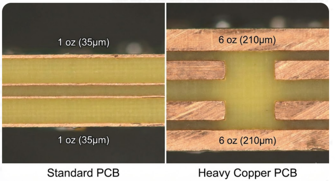
In my study, I discovered that in the PCB market, 1 oz/ft² (approximately 35µm) on the outer circuit boards and 0.5 oz/ft² on the inner circuit boards is typically referred to as standard copper weight. Another design that reverses the traditional is the use of copper weights of 3 oz/ft² (105µm) or higher, and in some radical designs, up to 20 oz/ft² or more. It is not a typo - we are talking of copper layers that are nearly a millimeter deep on one side of your heavy copper PCB.
You may ask yourself what kind of person could require that much copper. Physics is the answer. Conductor cross-section is directly proportional to the current-carrying capacity. A trace capable of safely carrying 1 A at 1 oz copper can safely carry around 3 oz copper at the same width, and the same at progressively higher copper concentrations. In the case of power electronics applications where tens or even hundreds of amperes are passing through the board, heavy copper is not an option; it is a necessity.
Heavy copper boards have several major differences from the normal PCBs. They need revised design guidelines (such as increased trace separation and annular rings) and alternative manufacturing techniques (etched and plated specialty), and the mechanical stress of the thick copper layers. The resulting product is a copper PCB that is physically stronger, heavier, and much more capable of high current, high temperature applications.
Key Uses in Power Electronics, Automotive, and Industrial Systems
Power electronics is simply based on heavy copper PCBs. As I have learned in class, they can be found everywhere- they can be found in the motor drive controllers that switch 50-200 A of phase current, the high power DC-DC converters used to power server farms or telecommunications equipment, and in EV battery pack management systems and inverters. You will also find them in industrial welding stations, power supplies, military and aerospace power distribution, and even in the controllers of solar and wind turbines.
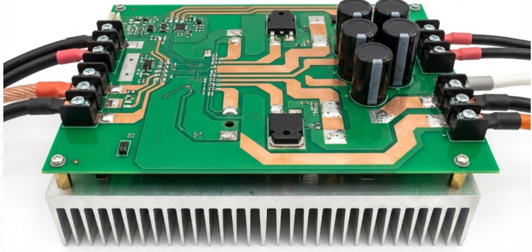
The trend of electrification in the automotive sector has increased the demand for thick PCB solutions. The onboard charger, DC-DC converter, and traction inverter of an EV require boards that can deal with large currents and dissipate significant heat in small enclosures. Those heavy copper boards are even more essential due to the reliability requirements, namely, AEC-Q standards, vibration resistance, and thermal cycling.
The other massive market is industrial automation. Servo drives, variable frequency drives, and power distribution panels are no longer being made using traditional busbar kits; instead, they are being implemented in PCB-based implementations, and it is the heavy copper that has enabled that.
Material and Structural Advantages of Thick Copper Layers
Enhanced Current Capacity and Reduced Resistance in Thick PCB Boards
The primary benefit of heavy copper on PCBs is straightforward: the more copper, the less resistance per inch, the higher the current capacity, and the less heat the conductor generates.
Consider a practical example. A 10mm-wide trace in 1 oz copper has a DC resistance of approximately 4.8 mΩ per centimeter at room temperature. The same trace in 4 oz copper drops to approximately 1.2 mΩ/cm, which is about 4x reduction. At 20A, the 1 oz trace would dissipate 19.2 mW/cm as I²R losses, while the 4 oz trace dissipates only 4.8 mW/cm. Over a 10 cm trace run, that difference of 144 mW may not sound dramatic, but multiply it across dozens of high-current traces on a power board, and the thermal impact becomes very significant.
Less resistance also implies reduced voltage drop across the power distribution traces, which is of paramount importance in maintaining tight regulations in precision power supplies, as well as to ensure that you will have adequate gate-drive voltage at the end of a long power bus.
Improved Heat Dissipation and Mechanical Strength
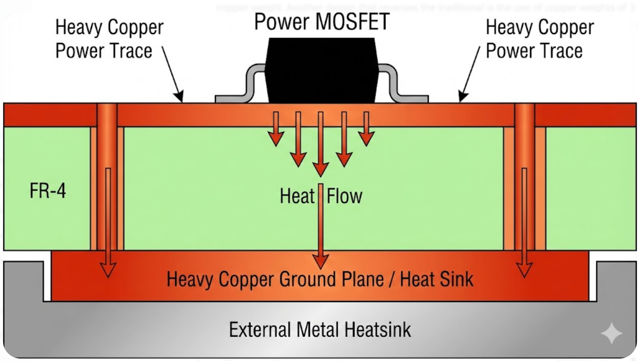
Copper layers are heavy, which serves as an internal heatsink. Copper thermal conductivity (approximately 400 W/mK) is far superior to FR-4 (approximately 0.3 W/mK), and thus a mass of copper provides low-resistance heat paths that conduct heat laterally across the board, beyond the hot components under power.
This thermal diffusion is particularly handy when you combine massive copper with thermal vias, which are connected to external heatsink areas. As an example, a set of thermal vias beneath a power MOSFET, connected to a heavy copper ground plane on the other side, can reduce the junction-to-board thermal resistance by a lot compared to a copper-based design.
The additional copper also provides the board with additional stiffness: the extra copper provides higher rigidity to the board, which prevents flexing, and enhances vibration resistance, which is significant in automotive and industrial boards, which are subjected to mechanical stress throughout the life cycle.
Copper Weight Specifications and Layer Integration Options
Heavy copper specs are most commonly expressed in ounces per square foot (oz/ft² ). The standard ones are 3 oz (105 µm), 4 oz (140 µm), 6 oz (210 µm), 10 oz (350 µm), and 20 oz (700 µm) in case of extreme requirements. The choice of which to pick will depend on the current amount you need to carry, the space you have available, and the capacity of your fab.
In case of layer integration, you can make each layer full-heavy (superior in pure power boards), or you can provide heavy copper power layers and standard-weight signal layers in a hybrid stack-up. This hybrid is becoming popular as it provides you with high-current capacity where you really need it and still allows you to route fine-pitch control signals on the standard layers.
JLCPCB has heavy copper selections and hybrid stack-ups that allow you to fine-tune power, as well as signal routing, on the same board.
Pro-Tip: When specifying heavy copper, always check that your fabricator can maintain the minimum trace width and spacing you need at your chosen copper weight. Etching tolerances increase with copper thickness, so a 6/6 mil trace/space design that works perfectly at 1 oz may need to be relaxed to 10/10 mil or wider at 4 oz.
Design Strategies for Optimal Heavy Copper Performance
Trace Width, Spacing, and Thermal Via Rules
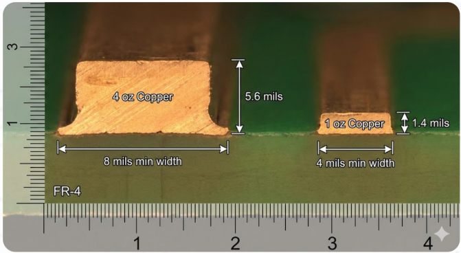
Hey boys, it takes a different rule of thumb when you are working with heavy copper. The etching of thick copper ends up diffusing a little (undercutting), thus the minimum size trace and spacing you can actually achieve is directly dependent on the copper thickness. Approximately, the trace width minimum in mils is approximately the same as the copper thickness in mils. Thus, 4oz copper (approximately 5.6mils thick) essentially limits your min trace width to about 6-8mils, and the separation is proportional to that. In the current-carrying traces, simply search the IPC-2152 specifications or any trace width calculator to choose the correct trace width depending on your current, desired temperature, and copper weight. I would always leave yourself some additional leeway - a temperature increase of 10°C is a good starting point with most projects.
In power components ( thermal via array ), use the largest via diameter you can manage (typically 0.30-0.5 mm) on a small pitch (1.0-1.5 mm center-to-center) to achieve the highest amount of copper heaving on the board. Fill and cap the vias, by your means--they will be soldered on to them anyway.
Balancing Power Distribution and Signal Integrity
The large copper designs frequently need to be able to support more than high-current power and finer control signals on a single board. The key ingredient is good zoning and stack-up. Assign power distribution (heavy copper) and other layers to signals (standard copper), and cover them with ground planes.
Separate the high-current power traces physically by keeping them physically apart with sensitive analog and high-speed digital traces. The high currents may introduce noise into adjacent signal traces due to the magnetic fields of the high-current paths, particularly when the return path is not kept tidy. Sewing the vias between the ground planes assists in constructing electromagnetic shields between the power and signal planes.
In the case of mixed stack-ups, a standard recipe is heavy copper on the outer layers (power bus) and standard copper on the inner layers (signals) and ground plane on the top and bottom of each signal layer. This configuration provides you with enormous current-carrying capability, good thermal conductivity, and clean routing of signals in a single board.
DFM Considerations to Avoid Common Pitfalls
Common failures in DFM of heavy copper designs include trace widths and spacings that are too narrow to accommodate the copper weight (DFM will raise a flag, but it will only delay your release), neglecting the additional board thickness when selecting connectors and enclosures, not re-sizing annular rings to the more relaxed drill-to-copper tolerance at higher copper weights, etc.
Hit up your fabricator early. Toss the stack-up specifications, copper weights, and minimum feature sizes overboard before you commit to design. Even a fast DFM convo can save you a lot of headache later on redesigning.
Advanced Manufacturing Processes for Heavy Copper PCBs
Precision Etching, Plating, and Lamination Techniques
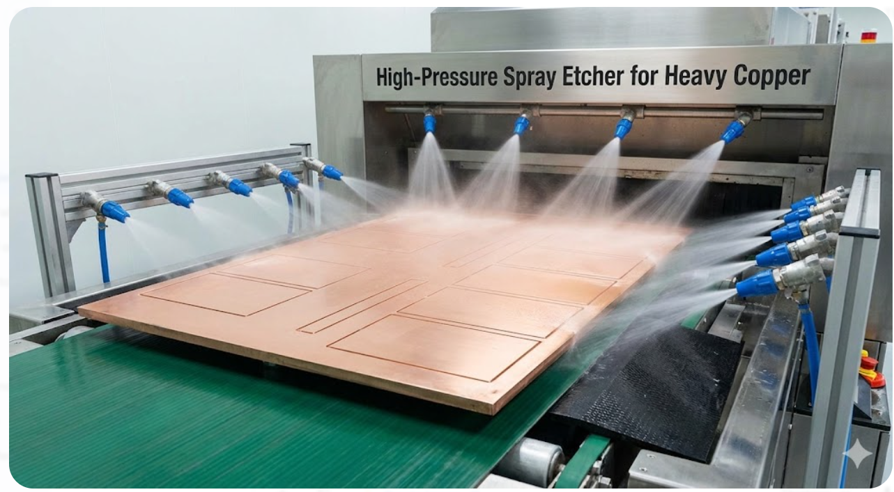
In the case of heavy copper PCBs, though, it is a different ball game altogether than the ones we normally find in the laboratory. A thicker copper requires more time in the etchant, and it results in the expansion of the etch along the sides, causing the loss of tiny features to be a nightmare. That is the reason why I have witnessed high-pressure spray etchers having the chemistry held in tight so that they can avoid undercutting and still nail a clean trace line.
Uniformity of plating is also a nightmare. Electroplating of these thick layers (the ones that are used in build-up fills or to add copper weight) must keep the size of the knife across the whole panel. The spread current, the bath chemistry, the agitation--all this has to be set precisely for heavy copper. When you miss one of those, you have a wavy copper surface, which is a no-go.
Wholesomely, another challenge is the lamination of heavy copper layers using prepreg and cores. The thermal mass of the thick copper interferes with the heat diffusion during lamination, and when the resin does not fill the space between the heavy copper pieces, you may get empty spaces that destroy reliability. I have seen skilled people operate modified press cycles that are specifically adjusted to heavy copper builds. It is just a matter of dragging the correct temperature and pressure curves.
Handling Thick Foils and Ensuring Uniformity
The usage of 3 oz or heavier foils disrupts the normal working process. They are too stiff to bend like the thin foils, and thus registration during lay-up is a high-stakes affair. To make it worse, the foils accumulate additional internal stress when laminated, and that may be warped or delaminated if you do not pay attention to it.
Other sophisticated fabricators combine plating and foils in order to reach the desired copper mass. Similar to, rather than begin with a 4 oz foil, you can plate a 2 oz foil with an additional 2 oz. In that manner, the initial foil is light and manageable, and you have the same overall weight and the same lack of headaches when handling.
Cross-sectional analysis at various panel locations will ensure that you are achieving the desired copper thickness at consistent panel locations. This is particularly important at the board edges or in dense and tight feature areas where the etch or plating can act out of the center of the panel.
Quality Controls for Reliability in High-Power Environments
Power gear with heavy copper boards receives a high-quality inspection on top of the PCB inspection. High-current tests ensure that the traces and the vias are able to remain at rated currents without overheating. The thermal cycling tests prove that these thick copper layers and solder joints can endure repeated temperature changes without delaminating or cracking.
The next level of critical microsection analysis of plated through-holes is required when heavy copper builds are involved, since the via barrel plating must be sufficiently thick and uniform to conduct the expected currents. The peel-strength test is then used to confirm that the copper is adhered to the substrate to ensure that the mechanical load that is added by the thick copper does not disrupt the bonding of the layer.
JLCPCB’s Expertise in Delivering Robust Heavy Copper Solutions
Cutting-Edge Equipment for Thick Copper Layering and Testing
JLCPCB fab shop. Hey, the fab shop of JLCPCB has everything: high-pressure spray etching lines, fine electroplating systems, and multi-daylight lamination presses, which are all oriented to heavy copper. It implies that regardless of whether you are placing orders of a small number of prototypes or bulk orders of full-sized batches of thick-copper PCB designs, you will receive the same results each time.
Customized Support from Prototyping to High-Volume Runs
It typically takes an iterative prototyping approach to power electronics projects to confirm thermal performance and current handling, then you lock in volume production. JLCPCB supports the entire process with fast-turn prototyping of heavy-copper boards, where you can test and refine your design in a short time before production. Both the prototype stage and the volume stage use the same production processes; hence, your proven prototype is easily transferred to mass production.
Proven Track Record in Power-Optimized PCB Board Fabrication

JLCPCB has produced heavy-copper boards for a large variety of power electronics devices, including motor controllers and solar inverters. That experience also implies that the engineering team actually knows the ins and outs of heavy-copper production and can offer you sound DFM advice, based on your project. Simply upload your design, and the DFM system will indicate possible problems prior to it emerging as a production problem.

Frequently Asked Questions (FAQ)
Q. What qualifies as a heavy copper PCB?
Any PCB with a copper weight of 3 oz/ft² (approximately 105µm) or more on any layer is generally classified as heavy copper. Some manufacturers set the threshold at 2 oz. Boards with copper exceeding 20 oz/ft² are sometimes referred to as “extreme copper” designs.
Q. How does heavy copper affect board thickness and weight?
Significantly. Each additional ounce of copper adds approximately 35µm of thickness per layer. A four-layer board with 6 oz copper on all layers is roughly 0.84mm thicker and substantially heavier than the same board with 1 oz copper.
Q. Can I mix heavy copper and standard copper layers in one board?
Yes, hybrid stackups are common and recommended for boards that need both high-current power distribution and fine-pitch signal routing. Heavy copper outer layers handle power, while standard inner layers carry signals.
Q. What are the minimum trace widths achievable with heavy copper?
Minimum trace width increases with copper weight due to etching limitations. As a general guideline: 3 oz supports approximately 5-6 mil traces, 4 oz supports approximately 7-8 mil, and 6 oz typically requires 10 mil or wider. Exact capabilities depend on your fabricator’s equipment and process.
Q. Is heavy copper more expensive than standard PCBs?
Yes. Heavy copper boards cost more due to increased raw material consumption, longer etching cycles, specialized plating, and more complex lamination. The premium varies with copper weight and layer count but typically ranges from 30% to 200% above comparable standard-copper designs.
Keep Learning
Your Ultimate Guide to PCB Rulers
In the world of PCB design and manufacturing, having the right tools is crucial for achieving accuracy and precision. One such tool that has gained popularity among professionals and hobbyists is the PCB ruler. This specialized measuring tool is designed to provide accurate measurements, reference information, and component footprints, assisting designers, engineers, technicians, and assemblers in various stages of PCB development. In this guide, we'll explore what a PCB ruler is, the features and mea......
Understanding the Materials Used in PCBs: Selection, Types, and Importance
Key Takeaways FR-4 is the go-to material for most cost-effective and reliable PCBs. Use Rogers for high-frequency and RF applications to reduce signal loss. Higher copper weight (2oz) improves current and heat handling. Choose High-Tg substrates for better thermal stability in multilayer boards. Green LPI soldermask offers the best balance of performance and inspection. Printed circuit boards (PCBs) are an essential component of modern electronics. These boards connect and support electronic component......
How to Select Tg of PCB ?
What is the Tg of PCB? In PCB manufacturing, "Tg" stands for Glass Transition Temperature. It is the temperature at which the PCB substrate material transitions from a rigid, glassy state to a soft, rubbery state. PCBs are flame-retardant (UL94 V-0) and do not burn easily; instead, they soften above Tg. The Critical Correlation Between Tg and Z-Axis CTE (Coefficient of Thermal Expansion) When the temperature exceeds the Tg point, the PCB substrate material (such as standard FR-4) undergoes a physical ......
How to Choose the Thickness of PCB
First, In the world of electronic products, the PCB is often referred to as the "heart" of the device. It interconnects all components, making board thickness one of the most important parameters. Choosing the right PCB thickness directly affects the electrical performance, mechanical stability, thermal management, and long-term reliability of the final electronic product. The process of selecting PCB thickness is influenced by various factors, such as product application scenarios, board material, an......
PCB Copper Pour Basics
What is Copper Pour in PCB Design? Copper pour refers to the technique of filling unused areas of a PCB's copper layers with solid copper planes. These planes are connected to power or ground nets, creating a continuous conductive path. Copper pour is typically used in the power and ground planes, as well as in signal layers for specific purposes. Purpose and Benefits of Copper Pour: Copper pour is primarily used to fill unused areas on PCB copper layers with solid (or hatched) copper connected to pow......
How to Prevent Solder Bridges for Superior PCB Quality and Reliability
Key Takeaways Solder bridges are a leading cause of SMT failures on fine-pitch components. Prevent them with proper solder mask dams (0.075–0.1mm), optimized stencil design, and controlled reflow profiles. Combine good DFM practices with AOI + X-ray inspection for maximum reliability. Professional manufacturing and early DFM review significantly boost first-pass yield and reduce costly rework. You have experienced the post-reflow sadness and eyed the board that failed on the first reflow, if you have ......