Can AI Really Design a PCB? Putting Claude Fable 5.2 to the Test
17 min
- Introduction
- Can AI Design a PCB? Fable 5.2 Test Results at a Glance
- How Fable 5.2 Designed the PCB in KiCad 10
- Fable 5.2 Test PCB: A BK7238 Wi-Fi and BLE Castellated Module
- From Datasheet to Schematic: How Fable 5.2 Read the BK7238 Reference Design
- Fable 5.2 PCB Layout: Placement, PCB Antenna, and RF Routing
- Fable 5.2 Design Verification: ERC, DRC, and Approved Exceptions
- Fable 5.2 PCB Manufacturing Files: Gerbers, Drill, BOM, and CPL
- Fable 5.2 Token Usage: How Many Tokens One PCB Design Took
- Can AI Design a PCB? What Fable 5.2 Did Well and Where It Needed a Human
- Conclusion
- FAQs About AI PCB Design

Introduction
Can AI design a PCB from datasheets to manufacturing files?
We put Fable 5.2 to the test with a real hardware design project, taking it through schematic capture, PCB layout, design rule checks, and Gerber generation in KiCad 10. The result was a complete manufacturing file set with every DRC error either resolved or explicitly approved. But does that mean AI can design a reliable, working PCB on its own?
Not quite. An engineer reviewed and approved each stage, rejected the model's initial component placement, and corrected three misinterpreted reference connections. Although the final deliverables included Gerbers, a bill of materials (BOM), and component placement files, the board has not yet been fabricated or physically tested.
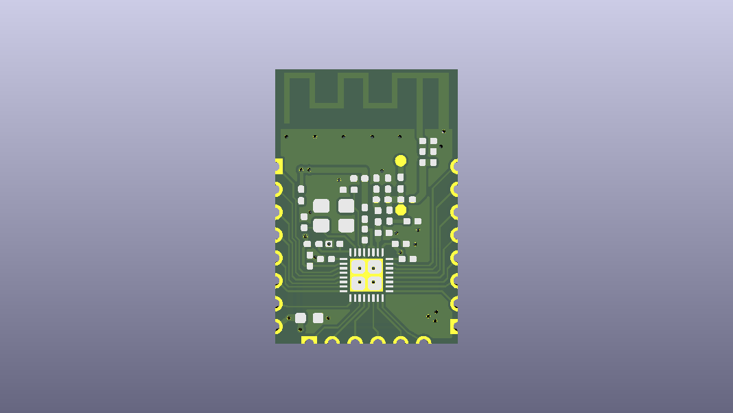
Figure: Top view of the BK7238 Wi-Fi module PCB in KiCad designed by Fable 5.2.
In this guide, you will learn:
- What AI achieved: The design files Fable 5.2 generated and what passing DRC actually proves.
- How the workflow operated: The step-by-step process from datasheets to Gerbers using KiCad 10.
- Where human intervention mattered: The placement decisions, circuit corrections, and engineering approvals.
- What the experiment cost: The total token usage, why cache reads dominated, and what the numbers reveal about AI-assisted PCB design.
Note
JLCPCB, Anthropic (Claude), and KiCad are not affiliated with PCB_Flow or the kicad-mcp-pro project and are not responsible for designs made with them. Whoever runs an AI-assisted design flow is responsible for the design and for the third-party tools, MCP servers, and models they choose, including checking every result before fabrication.
Can AI Design a PCB? Fable 5.2 Test Results at a Glance
Fable 5.2 completed every design stage, from requirements to release files, for a 16 × 24 mm, two-layer Wi-Fi and BLE module.
| Design Task | Fable 5.2 Result | What It Does Not Prove |
|---|---|---|
| Part selection | 18 fitted parts with LCSC codes; basic parts wherever one met the requirement | Part stock, which was not re-checked before release |
| Schematic | ERC with 0 violations; a custom 32-pin BK7238 symbol that matches the datasheet pin table | A readable drawing; the engineer corrected three reference-sheet connections |
| Placement | Rev B approved after the engineer rejected Rev A | How far the antenna detunes on this board |
| Routing | 0 unconnected items, 0 clearance or short errors | RF line impedance, which is an estimate |
| DRC review | 216 items explained; four exceptions approved by the engineer | That the narrowed PA supply trace is harmless under load |
| Manufacturing files | 6 Gerbers, a drill file, a job file, and a JLCPCB-format BOM and CPL | Gerber content in a viewer; the files were checked by content only |
| Hardware | Not fabricated, not bench-tested | Anything that needs a VNA or a powered board |
How Fable 5.2 Designed the PCB in KiCad 10
Fable 5.2 performed the design work in KiCad 10.0.4, and an engineer approved each stage before the next one began. PCB_Flow is an independent KiCad design panel we built, which sets the fixed stages and holds the model at each approval gate.
The model reads and edits the KiCad project through kicad-cli and an MCP (Model Context Protocol) server. The panel can run Claude or ChatGPT/Codex models; this test used Fable 5.2 throughout. A full PCB_Flow guide will follow once the tool is open to everyone.
For a general setup, see our KiCad MCP guide, and for a similar test in EasyEDA Pro, see Claude Code PCB design.
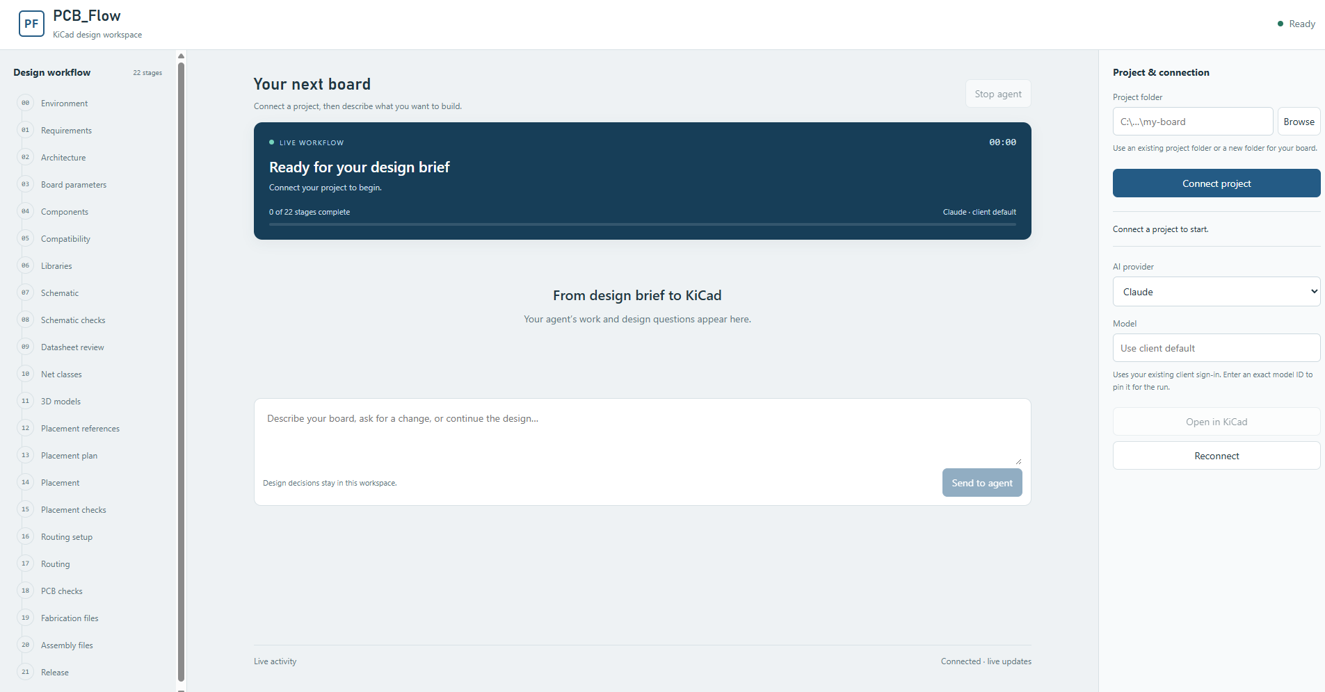
Figure: PCB Flow panel in KiCad with the 22-stage design workflow and the AI provider selection.
The 22 stages fall into six groups:
- Setup and requirements: environment check, requirements, architecture, and board parameters
- Parts and libraries: component selection, compatibility checks, and the symbol and footprint libraries
- Schematic: schematic capture, schematic checks, and a datasheet review
- Placement: net classes, 3D models, placement references, placement plan, placement, and placement checks
- Routing and checks: routing setup, routing, and PCB checks
- Release: fabrication files, assembly files, and the release record
Each stage saves its evidence as notes. Choices that belong to the engineer, such as the layer count, appear in the panel as questions; this design logged 12 decisions, D1 to D12.
Fable 5.2 Test PCB: A BK7238 Wi-Fi and BLE Castellated Module
The main test was a standalone Wi-Fi 4 and BLE module built around the Beken BK7238, a 4 × 4 mm QFN32 chip with a 0.4 mm pin pitch. An on-board antenna makes it a demanding layout test.
The project started from our own need for a low-cost, reliable Wi-Fi and BLE option for our IoT devices, in the same role as the ESP modules. The BK7238 is a low-cost Wi-Fi 4 and BLE chip. We asked Fable 5.2 to design a castellated module around it on the familiar ESP-12F footprint, with 22 pads at 2.0 mm pitch. Only the VBAT and GND pads keep their ESP-12F positions, so the module is footprint-compatible with an ESP-12F but not pin-compatible.
| Parameter | Value |
|---|---|
| Board size | 16.00 × 24.00 mm, 0.8 mm thick |
| Layers | 2 (F.Cu, 0.73 mm FR-4 core, B.Cu), 1 oz copper, ENIG |
| Edge connection | 22 castellated pads at 2.0 mm pitch, ESP-12F footprint pattern |
| Main chip | BK7238QH321, QFN32, 4 × 4 mm, 0.4 mm pitch |
| Antenna | 2.4 GHz meandered inverted-F PCB antenna |
| Clock | 26 MHz crystal, 9 pF load, 3225 package |
| References | 33: 18 fitted, 9 unfitted tuning positions, 6 copper-only items |
| Build plan | Bare boards with a stencil, hand assembly, 5 to 10 pieces |
Fable 5.2 received five inputs:
- The BK7238 chip datasheet
- The ME16WS02 module datasheet
- The Beken reference schematic, revision 1.2
- Photos of a reference module's component placement
- A completed hand-over prompt with the board requirements
From Datasheet to Schematic: How Fable 5.2 Read the BK7238 Reference Design
Fable 5.2 turned the datasheets into a requirements list, a parts list, and a schematic that passed ERC with 0 violations. The engineer still had to settle the layer count and correct three connections that the model had misread from the reference sheet.
Requirements and Part Selection
The engineer requested basic parts from the JLCPCB Parts Library to avoid extra assembly charges. Fable 5.2 followed that rule and documented each exception:
- Basic where possible: the exceptions, each with a stated reason, were the BK7238, the 26 MHz crystal, the 3.6 nH RF inductor, the 18 Ω PLL supply resistor, and three RF capacitors from the Preferred class.
- Alternative offered: for the 18 Ω resistor, the model offered a Basic 22 Ω part and calculated the shift in the PLL supply filter; the engineer kept the 18 Ω reference value.
- Layer count: the model recommended 4 layers. The engineer chose 2 layers at 0.8 mm, and the model switched to Beken's 2-layer layout rules.
- Crystal load: with no 7–8 pF, 26 MHz crystal at LCSC, the model chose a 9 pF part. It meets the chip datasheet's 9 pF maximum but not the Beken sheet's 7–8 pF note, and the model flagged it as the largest electrical risk.
Custom BK7238 Symbol and Schematic: Correct Connectivity, Poor Readability
Fable 5.2 generated a custom BK7238 symbol from the datasheet pin table. All 32 PINs and primary pin names match the datasheet, and the exposed pad connects to ground.
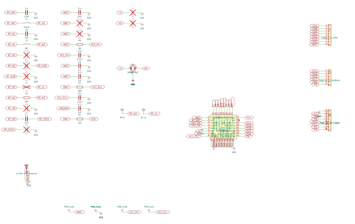
Figure: BK7238 module schematic drawn by Fable 5.2, with correct connectivity but parts scattered as label-linked fragments.
Schematic readability is where the model fell short. The connections are correct, but the sheet is hard to read:
- Fragmented circuit: Each passive sits on its own short wire between net labels, so the RF chain from the ANT pin to the antenna has to be traced label by label.
- Crowded symbol: The pin names on the custom QFN32 symbol overlap each other at the chip body.
- No signal flow: Supply filters, RF match, crystal, and edge pads sit in separate columns rather than flowing from input to output.
A schematic is also a review document. ERC confirms connectivity, but checking design intent depends on a drawing that an engineer can read at a glance.
Fable 5.2 PCB Layout: Placement, PCB Antenna, and RF Routing
Fable 5.2 placed and routed the board on two layers, but its first placement crowded the antenna. The engineer rejected it, and the approved second version moved the RF parts away from the antenna ground edge.
Placement Rev A Rejected, Rev B Approved
Rev A left the lower board largely empty, and the parts near the antenna posed a risk of parasitic coupling.
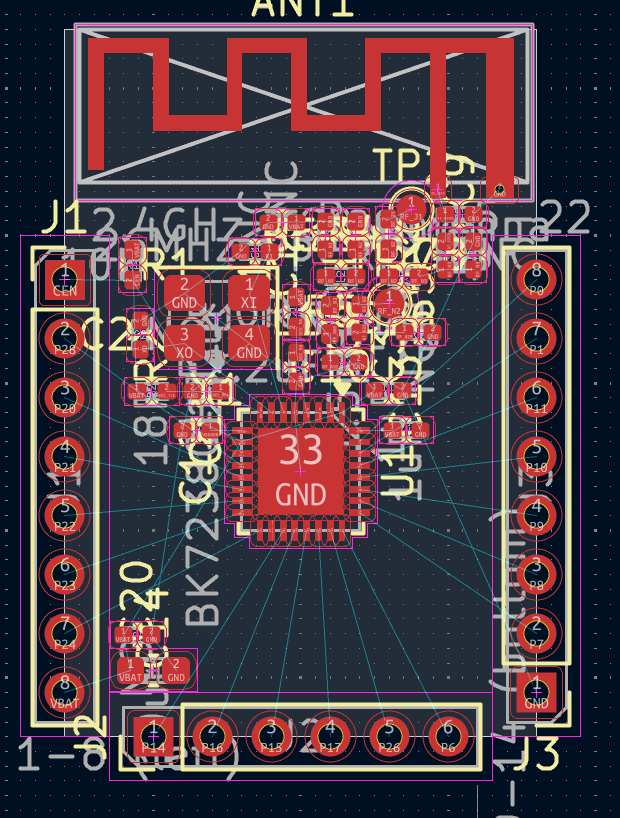
Figure: Rejected placement Rev A, with the BK7238 RF parts crowded against the antenna.
| Placement Measure | Rev A | Rev B |
|---|---|---|
| Chip position | Starting position | Moved 3.0 mm away from the antenna |
| Parts in the 4 mm strip below the antenna | 12 | 4: the antenna match C7, C8, C9, and test pad TP2 |
| Nearest other part to the antenna ground edge | 1.0 mm | 4.0 mm |
| Test pad TP2 to the antenna ground edge | 0.4 mm | 2.3 mm |
| PA supply trace | Along the antenna ground edge | Crosses 4 mm from the edge |
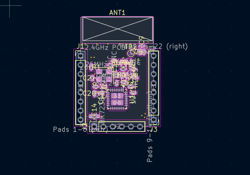
Figure: Approved placement rev B, with the chip cluster moved down to clear the strip below the antenna.
Fable 5.2 also found a gap in its own rev B: the VBAT supply pin (pin 10) had no capacitor next to it. It proposed fitting the spare C20 position with a 1 µF component and asked first because the change altered the approved parts list. The engineer agreed.
PCB Antenna and RF Match Network
Fable 5.2 did not design its own antenna. It used KiCad's library footprint of the inverted-F antenna from TI application note AN043 (SWRA117D) and confirmed a 0.8 mm margin to each side edge of the 16 mm board.
The RF match follows the Beken sheet: L1 3.6 nH, C4 1.5 pF, C6 1 pF, and C7 1 pF, plus unfitted positions C8 and C9 for tuning. The model recorded two limits:
- Footprint not checked against the TI drawing: the model could not open the PDF, so the footprint is KiCad's drawing of the note, not checked dimension by dimension.
- Detuning: TI designed the antenna on its own board. On 0.8 mm FR-4 with a smaller ground area, it is expected to detune by an amount that only a VNA measurement can show.
Two-Layer Routing and Supply Deviations
The routed board has 181 track segments and 28 0.30 mm vias. The RF path runs on the top layer only, with no bottom trace under it, and the 19 GPIO signals reach the edge pads on the top layer without crossings.
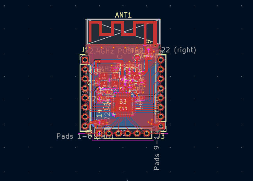
Figure: Routed BK7238 module in KiCad, with top copper in red, bottom copper in blue, and ground fills kept out of the antenna area.
Two supply traces break the approved width rules. Fable 5.2 reported both and asked for approval:
- Bottom supply branches at 0.3 mm instead of 0.5 mm: a 0.5 mm trace did not clear the ground vias next to the GND pad. The model calculated a drop of 10 mV or less at 270 mA, the datasheet's typical TX current, and these branches do not carry the PA current, which flows on the 0.5 mm branch.
- PA supply neck at 0.25 mm for 2.0 mm: Beken recommends wider than 0.4 mm. The channel between C10 and C4 is 0.56 mm, so 0.25 mm is the widest trace that keeps 0.15 mm clearance; a wider trace needs a placement change.
Fable 5.2 Design Verification: ERC, DRC, and Approved Exceptions
The final board passed ERC with 0 violations and DRC with 0 unconnected items and 0 clearance or short errors. KiCad still listed 216 DRC items, and each one traces back to a design choice the engineer reviewed.
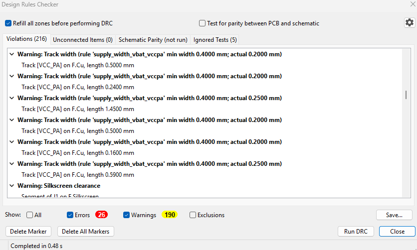
Figure: KiCad DRC result for the BK7238 module, showing 216 violations, 26 errors, 190 warnings, and 0 unconnected items.
| DRC Item | Count | Cause | Status |
|---|---|---|---|
| Copper-to-edge errors | 22 | Castellated pads sit on the board edge by design | Approved exception |
| Courtyard overlap errors | 4 | Test pad TP1 on the RF line overlaps four-part courtyards | Approved exception |
| Track-width warnings | 31 | 17 short necks into chip and 0402 pads, plus 14 segments on the two supply deviations | Reviewed and approved |
| Silkscreen warnings | 159 | Overlapping reference text; no silkscreen layer is exported (D12) | Not in the fabrication files |
| Total | 216 | 26 errors and 190 warnings | All reviewed |
Fable 5.2 PCB Manufacturing Files: Gerbers, Drill, BOM, and CPL
Fable 5.2 exported a complete file set for fabrication and a later assembly order, and it fixed a unit problem in KiCad's placement export.
The release contains:
- Gerbers: copper and solder mask for both sides, top paste, and the board outline, with no silkscreen layer by decision
- Drill and job files: one plated drill file with 51 holes (28 vias, 1 antenna ground hole, 22 edge holes) and a job file
- BOM: 18 fitted parts in JLCPCB columns with LCSC codes
- CPL: the placement list for the same 18 parts, in millimeters
- Documents: a 3D render, the schematic, a board PDF, and the decision log
KiCad's position export came out in inches and listed unfitted parts. Fable 5.2 rebuilt the CPL from the schematic in millimeters and checked five part centers against their pad midpoints.
Note
To create these files for your own board, see how to generate the BOM and centroid file from KiCad. The model checked the Gerbers by file content, not in a Gerber viewer. The BOM and CPL are kept so the same board can move to PCB assembly later.
Fable 5.2 Token Usage: How Many Tokens One PCB Design Took
The design used 52.3 million tokens across 343 model requests, and setup used another 13.3 million across 54 requests. About 95% of the design tokens were cache reads, the lowest-cost token type.
| Token Measure | Setup | Design |
|---|---|---|
| Model requests | 54 | 343 |
| Fresh (uncached) input | 130 | 686 |
| Cache write | 1,059,095 | 2,265,645 |
| Cache read | 12,183,313 | 49,530,929 |
| Output (of which thinking) | 63,151 (27,685) | 542,935 (309,387) |
| All tokens | 13,305,689 | 52,340,195 |
| Tool calls | 80 | 817 |
| Sessions | 1 | 12 |
Setup covers the hand-over prompt, reading the datasheets, and setting up the panel. Design covers panel stages 00-21. Each token type means:
- Fresh input: new text that is not already in the model's cache
- Cache write: project context, such as stage instructions and datasheet text, stored the first time the model reads it
- Cache read: the model re-reading that stored context on each request; providers typically bill it at a small fraction of the fresh-input rate, because the context is already processed.
- Output: the text the model writes, including its internal reasoning (thinking)
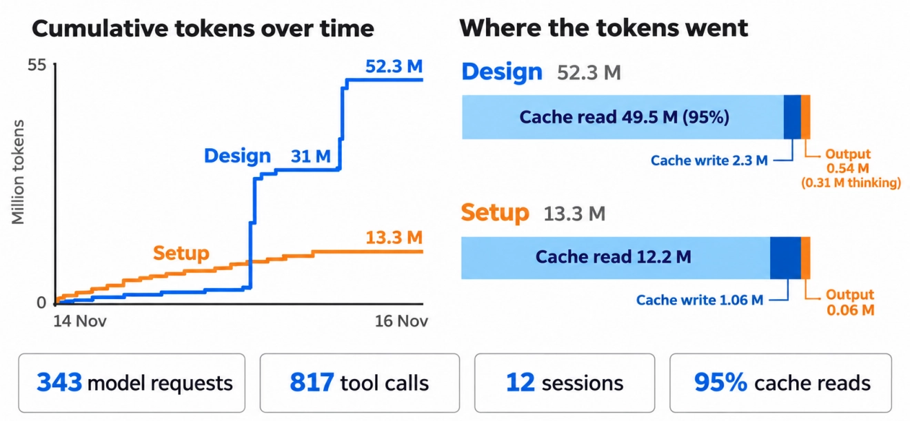
Figure: Cumulative Fable 5.2 tokens over the run and the split by token type: 52.3 M for design and 13.3 M for setup, mostly cache reads.
For the design stage, each request re-read about 144,000 tokens of stored context and wrote about 1,580 new tokens. Reasoning took 57% of the output. The design spanned about 6 hours of wall-clock time, including waits for approvals. Token usage was higher than is practical for routine work, so a second, more token-efficient version of PCB_Flow has since been built.
Can AI Design a PCB? What Fable 5.2 Did Well and Where It Needed a Human
Fable 5.2 reasoned well through a staged design and stated what it had not verified. It still required an engineer for key decisions, reference sheet corrections, and drawing quality.
What Fable 5.2 Did Well
- Reasoning with numbers: it backed each trade-off with a calculation, such as the voltage drop on a narrowed supply trace or the filter shift from a Basic resistor.
- Step-by-step flow: it worked through 22 stages in order and kept evidence notes for each, so a stopped run resumed without repeating work.
- Plain-language instructions: PCB_Flow's stage instructions are written in plain language, and the model followed them stage by stage.
- Questions before guesses: it raised 12 decisions, from layer count to silkscreen, and asked for approval instead of guessing, including deviations from rules it had set itself.
- Stated limits: each stage note lists what was not verified, such as the unopened TI PDF, the unviewed Gerbers, and the crystal pad map.
Where the Engineer Stepped In
| Task | Fable 5.2 | Engineer |
|---|---|---|
| Layer count | Recommended 4 layers | Chose 2 layers at 0.8 mm |
| Reference schematic | Misread three connections | Corrected them in D9 |
| Placement | Crowded the antenna in rev A | Rejected rev A, approved rev B |
| Pin 10 decoupling | Found the missing capacitor | Approved fitting C20 with 1 µF |
| DRC review | Listed and explained all 216 items | Approved four exceptions |
| Silkscreen | Reported overlapping reference text | Chose no silkscreen layer (D12) |
| Schematic readability | Correct but fragmented drawing | Not yet solved |
Verdict: Can Fable 5.2 Design a PCB on Its Own?
Fable 5.2 is a capable PCB design assistant. It can carry a design to manufacturing files under engineer supervision, but it does not yet replace the engineer's review.
Its connections and checks were sound, while its schematic and symbols were accurate but hard to read. To become more capable, it needs more training on PCB design or a dataset of reviewed designs to learn from.
For other AI tools at each design stage, see AI tools for PCB design guide.
Conclusion
AI can design a PCB up to manufacturing files: Fable 5.2 took a BK7238 Wi-Fi module from datasheets to Gerbers, BOM, and CPL, with an engineer approving each stage and every DRC exception. Use it as a staged assistant behind human approval gates, and treat each passed check as a file-level result until the board is tested. Fabrication, assembly, and hardware testing remain the next steps toward validating the design.

Whether you designed it manually or with AI assistance, upload your Gerber files and BOM to JLCPCB to get an instant quote for PCB fabrication and assembly.
Move from digital design to a physical prototype and put your circuit to the test.
FAQs About AI PCB Design
Can AI Design a PCB Without a Human?
Not yet. In this test, Fable 5.2 needed an engineer to choose the layer count, correct three reference connections, reject a placement, and approve four DRC exceptions.
Did the Fable 5.2 Board Work?
Not known yet. The module is designed and passes DRC with approved exceptions, but it has not been fabricated, so antenna tuning, TX power, and crystal frequency remain unproven.
How Many Tokens Does AI Need to Design a PCB?
This BK7238 module used 52.3 million tokens for the design and 13.3 million for setup. About 95% of the design tokens were cache reads, which are typically billed at a fraction of the fresh-input rate.
Can AI Design an RF PCB with an Antenna?
Only as far as the layout. Fable 5.2 placed a TI inverted-F antenna and the Beken match network, but tuning and RF line impedance need a VNA measurement on a built board.
Which PCB Design Software Did Fable 5.2 Use?
KiCad 10.0.4. Fable 5.2 worked on the live project through the kicad-mcp-pro MCP server and kicad-cli, guided by the PCB_Flow panel with an approval gate at each stage.
Popular Articles
• How to Design Your Own Keyboard PCB: From Layout to Firmware
• GPT-6 Astra PCB Design in EasyEDA Pro: What Worked, What Failed, and What We Learned
• Altium MCP with Claude Code: From Setup to PCB Design
• KiCad MCP: How to Design a PCB with Claude Code [Step-by-Step]
• Altium MCP: AI PCB Design with GPT-6 and Codex [Step-by-Step Guide]
Keep Learning
Can AI Really Design a PCB? Putting Claude Fable 5.2 to the Test
Introduction Can AI design a PCB from datasheets to manufacturing files? We put Fable 5.2 to the test with a real hardware design project, taking it through schematic capture, PCB layout, design rule checks, and Gerber generation in KiCad 10. The result was a complete manufacturing file set with every DRC error either resolved or explicitly approved. But does that mean AI can design a reliable, working PCB on its own? Not quite. An engineer reviewed and approved each stage, rejected the model's initia......
PCB Terminal Blocks : A Design Engineer’s Guide to Reliable Wire-to-Board Connections
Key Takeaways Address Failure Modes: Select proper clamps and mounts to stop loose wiring, joint fatigue, and arcing. Screw vs Spring: Screw blocks provide strong clamping for high vibration, while spring blocks speed up wiring. Safety Distances: Keep proper clearance distances for voltages over 15V to prevent electrical arcing. Optimized Footprint: Use larger annular rings and 2 oz copper to handle mechanical strain and heavy currents. Automated Assembly: Selective wave soldering prevents cold joints......
PCB Panelization Explained: Tips and Techniques
PCB panelization is a crucial process in modern electronics manufacturing, designed to streamline production and reduce costs. In this way smaller circuit boards are produced in bulk and joined to one another to form a single array. This bulk production fosters the easy movement of PCBs through an assembly line. CNC (Computer Numerical Control) machines are utilized in PCB production and assembly facilities. These CNC machines can design PCBs that are rather large in size. But typically, electronic pr......
PCB Card Edge Connectors : Design Essentials, Gold Finger Optimization, and Manufacturing Strategies for Reliable Integration
PCB card-edge connectors are the unsung heroes of modular electronics. By providing a gold-plated finger interface along a circuit board edge, they allow plug‑and‑play connections between motherboards, expansion cards, and memory modules. Unlike soldered or wired joints, card-edge contacts offer easy replacement and upgrade of components. You imagine swapping a graphics card or SSD by simply unplugging one board and plugging in another. This edge-based interconnect enables high-speed, high-density rou......
How to Design a PCB with Flux.ai (Step-by-Step Guide)
Key Takeaways This step-by-step Flux PCB design tutorial demonstrates the complete workflow by creating a compact 15 × 15 mm USB 2.0 hub, refining the layout, routing high-speed differential traces, and preparing manufacturing files for JLCPCB PCB fabrication and assembly. We are all hearing news; new AI models are being released every month. And it has finally reached the schematic editor. Flux.ai is a browser-based AI PCB design tool with a built-in AI agent that behaves like a junior hardware engin......
Mastering PCB Footprints: Design Best Practices for Reliable Manufacturing
Key Takeaways A PCB footprint (land pattern) translates component datasheet dimensions into copper pads, solder mask openings, paste apertures, silkscreen, and clearance areas that enable reliable soldering and assembly. Follow IPC-7351 standards and manufacturer DFM rules for pad dimensions, spacing, and layer design to minimize defects like solder bridging, tombstoning, and cracked joints. Choose between through-hole (THT) and surface mount (SMT) footprints based on electrical needs, thermal perform......