
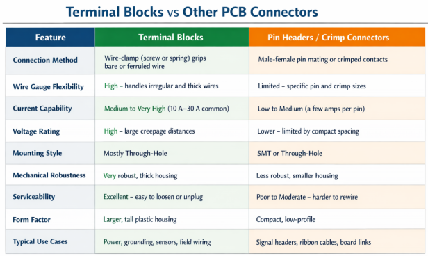
PCB Terminal Blocks : A Design Engineer’s Guide to Reliable Wire-to-Board Connections
15 min
- What Is a PCB Terminal Block?
- Types of PCB Terminal Blocks
- Key Factors When Choosing a PCB Terminal Block
- PCB Design Considerations for Terminal Blocks
- Assembly Methods and Soldering Best Practices
- Reliability, Performance, and Common Mistakes
- How JLCPCB Supports Reliable Wire-to-Board Connections
- Frequently Asked Questions (FAQ)
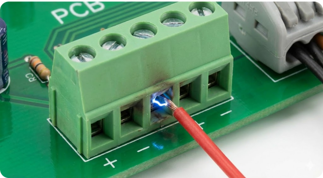
PCB terminal blocks are the unsung heroes of wire-to-board connections. They can be used to connect or replace wires in industrial controls, power supply, and automotive systems, etc, without needing to re-work the PCB. Terminal blocks can be tight-clamped or screwed, eliminating the guesswork of hand-soldering. However, terminal blocks may be problematic. Loose wiring can vibrate, heavy elements can be subject to solder-joint fatigue, and a lack of creepage or clearance can allow arcs to arc between traces. The loosely screwed screw will vibrate and have intermittent malfunctions, whereas the clearance that is too small may permit arcs during wet weather. Early detection of these problems can be achieved by the selection of an appropriate block type, adherence to spacing regulations, and stiffening heavy mounts. A good wire-to-board solution prevents trace burn-outs and eliminates late-night debugging.
The Critical Role in Wire-to-Board Connections for Industrial, Power, and Control Projects
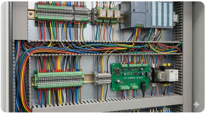
Terminal blocks shine in demanding applications. They’re built to handle high currents and harsh environments that would overwhelm simple pin headers or IDC cables. In control panels and industrial automation, for instance, PCB terminal blocks are everywhere: connecting motor drives, sensors, power supplies, and ground buses. On heavy machinery and in aerospace systems, terminal blocks tame the thick-gauge wires that carry motor power or 48 VDC rails. Even in consumer electronics, they pop up in power supply units where reliability is key.
These connectors allow engineers to mount large-gauge wires (large compared to PCB connectors) and strip and clamp large conductors rapidly. Terminal blocks provide flexibility to the designer because they have a vast array of wire sizes and types; you can mix solid-core and stranded wire, different gauges, and different numbers of conductors, all without redesigning the PCB. They are also easier to maintain- faulty boards are not desoldered to be unplugged from the field wiring, which reduces downtime.
A low and high-voltage enclosure can be put into a single enclosure. Isolate the PCB wiring of each domain so that they do not touch. It is important to note that once any conductor pair reaches approximately 15 V, the creepage and clearance are required to be increased in accordance with safety standards like IPC2221.
Addressing Pain Points: Loose Wiring, Solder-Joint Failures, and Creepage Distance
A properly designed terminal block can fail if it is installed poorly or designed poorly. Loose connections are an infamous pain in the neck: a loose wire on a screw that is clamped may not be noticed until it starts to intermittently act or arc. This issue is particularly prevalent in machine vibration-prone equipment. It is important to properly torque screws or provide spring clamps with the required level of vibration, with a particular expectation. Other engineers use thread-lock or insert wire ferrules on strand wires to ensure they are not corroded and do not slip.
Solder-joint fatigue is another issue. Large terminal blocks are heavy, and their metal posts create a significant thermal mass. A thin pad or inadequate solder can crack under thermal cycling or mechanical stress. Using through-hole, wave-solderable blocks with ample copper pads helps form a strong fillet that resists flexing. In automated assembly, heavy components like terminal blocks often receive a selective solder or wave solder operation to ensure full wetting. Manual soldering, by comparison, is error-prone. In fact, JLCPCB notes that hand-soldered boards can suffer from “cold joints and inconsistent wetting,” especially on chunky connectors.
Finally, creepage and clearance distances must never be ignored in power applications. Creepage is the distance along the insulating surface between conductors, while clearance is the shortest through-air distance. High voltages can arc if these gaps are too small. Industry guidelines specify minimum spacing. In practice, a 230 VAC system may require 5–10 mm creepage on FR-4; more if there’s moisture or dirt. Always consult the relevant tables. Even with the correct creepage, it’s wise to mark HV terminals on the silk screen and route their wiring away from signal traces. In one project, an oversight in spacing caused a tiny spark to bleed into a nearby sensitive analog trace, introducing noise that mystified the team for days. Better safe than shorted!
What Is a PCB Terminal Block?
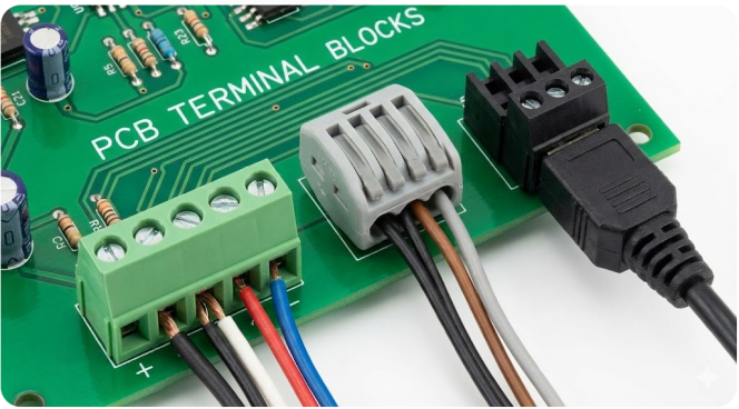
A PCB terminal block is essentially a modular, insulated connector that clamps wires to a board without requiring soldering. Think of it as a removable junction point: each block has metal terminals. Wires are inserted and fastened at the top, while the bottom of the block is soldered or otherwise attached to the PCB copper. This design provides both electrical contact and mechanical retention. Unlike fixed connectors, terminal blocks are designed for wire-to-board duty. They handle larger conductors and higher currents than typical board connectors.
Many terminal blocks are also removable or DIN-rail compatible. For example, a 12-position terminal block might be one solid piece, or it might consist of a soldered “header” base and a plug-in terminal. They ensure that current flows directly from external cables into the board copper without intermediate bulky wiring. Terminal blocks often sit at the edge of the PCB or on a mounting bracket, where they align with chassis wiring harnesses.
Differences from Other Connectors and Common Applications
Terminal blocks differ from other connectors in a few key ways:
Types of PCB Terminal Blocks
Screw Terminal Blocks for Secure, High-Vibration Use
Screw terminal blocks (also known as screw-down or clamping blocks) use metal screws or bolts to press the wire against a conductive plate. They’re the classic design: strip the wire, lay it in the slot, then tighten the screw to lock it. This type is prized for mechanical reliability. A properly torqued screw won’t let go unless you loosen it, making it ideal for high-current and high-vibration environments. In fact, experts note that through-hole screw-terminal blocks “provide better stability” under vibration than other types.
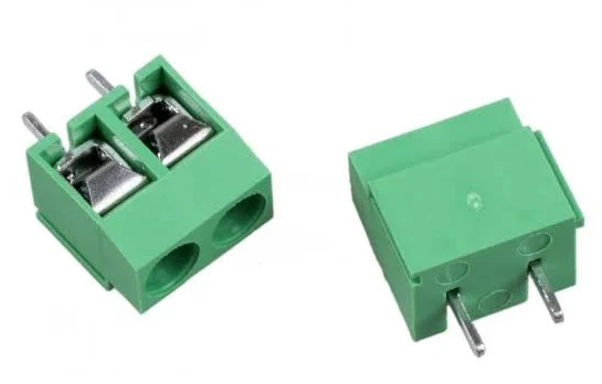
Screw blocks come in many pitches; the common values are 3.5 mm, 5.08 mm, and 7.62 mm. The pitch determines how thick a wire/gauge it can accept. Larger pitches accommodate bigger wires. They also usually have a rugged plastic housing rated to UL94-V0 and often are available with locking levers or captive screws to prevent parts loss. Because of the screw mechanism, installation takes a bit longer, but the connection is a rock-solid clamp.
Spring Clamp and Push-In Variants for Quick Wiring
Spring-terminal blocks replace the screw with a metal spring that you activate (usually by pushing a lever) before inserting the wire. When you release it, the spring clamps down on the conductor. Push-in blocks work similarly but may lock automatically when you insert the wire. These designs are much faster to wire up: insert the wire and let go, and it snaps in. They’re often found in control cabinets and wall-mounted equipment where field changes are frequent.
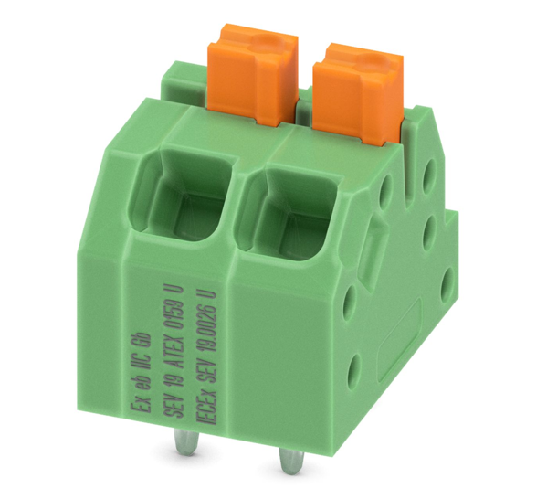
According to industry guides, spring and push-in blocks “offer faster assembly” and are great for applications where wires might be reconfigured. The trade-off is that they generally handle slightly less current and may not hold quite as firmly under extreme vibration. However, good designs apply strong spring forces and often provide easy-release levers. Typical pitches are similar to screw blocks 3.5 mm and 5.0 mm. When using spring terminals, ensure the conductor is fully inserted under the spring claw. A common mistake is leaving a small tail out, which can spring loose. Also, remember that stranded wire should often use ferrules when used with spring clamps for maximum grip.
Pluggable Terminal Blocks for Maintenance Efficiency
Pluggable terminal blocks integrate two-piece springs or screws. It will consist of a PCB-mounted header and a removable wiring plug. To unplug, simply unplug the plug, all the wires off the board simultaneously. To reconnect, all you need to do is reinsert the block. This proves to be very convenient where it is needed in the field or where the boards are to be hot-swapped.
Pluggable terminal blocks are designed to ensure that any maintenance becomes as easy as changing a connector. A pluggable block may be a part of each board in a multi-board control system. Thereby, in case of a board failure, you can unplug the wires, replace the board, and reconnect them without having to re-solder the wires. The base is either through-hole or SMT, with the plug being at a right-angle orientation to ease cable routing. There are other plugs that are two-way fitting, though the majority of plugs are keyed to fit in a single direction.
Key Factors When Choosing a PCB Terminal Block
Electrical Ratings, Mechanical Strength, and Environmental Resilience
Selecting the right terminal block starts with electrical requirements. The block’s current rating must exceed the maximum your design will carry, typically by a safe margin. Always leave a 20–30% safety buffer over your expected load. For example, a 10 A motor circuit might use a 15 A terminal block to account for surges. In general, blocks for heavy power start around 15–20 mm pitch and can carry tens of amps, while small-signal blocks might be 3–5 mm pitch at only 2–5 A. The wire size compatibility is linked to these ratings. Terminal blocks specify an AWG range (28–16 AWG for a small block, 20–6 AWG for a power block). A too-small wire will wobble and produce a poor connection; a too-large wire simply won’t insert.
Mechanical factors include vibration and shock. The clamp mechanism should resist loosening – high-vibration applications often favor screw types with locking washers or double-screw blocks. Some spring designs may work loose if a wire is intermittently tugged, so confirm the retention force. Also, look at the housing material: polyamides with UL94 V-0 flammability rating protect against fire, and blocks with IP ratings or conformal-coated options can survive moisture and dust.
Checklist:
- Verify current and voltage ratings (add 30% margin).
- Match the wire AWG range to the block spec.
- Ensure mechanical mounting is robust.
PCB Design Considerations for Terminal Blocks
Footprint Layout and Creepage/Clearance Rules
When placing terminal blocks on your PCB, plan the footprint carefully. Use the exact land pattern from the manufacturer’s datasheet. Ensure that pad and hole sizes follow IPC guidelines for through-hole blocks. This means allowing a proper annular ring around each lead. For example, IPC-2221 requires a certain annular ring and fabrication allowance to ensure durability. In practice, this might mean adding 0.4–0.6 mm beyond the hole diameter on each side. A generous pad helps distribute solder and provides a solid anchor.
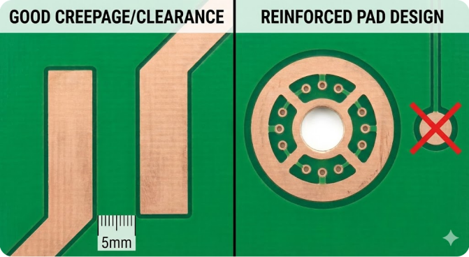
Spacing is equally critical. Maintain adequate clearance and creepage between the block’s conductive parts and any nearby conductors. As a rule of thumb, once the voltage difference exceeds 15 V, IPC‑2221 mandates specific spacing. High-voltage terminal blocks may require several millimeters of clearance to the next copper feature. If creepage is tight, you can increase it by adding board slots or insulating barriers between pins. The Altium high-voltage guide notes that cuts or slots can effectively lengthen the creepage path without changing your trace routing.
Also, watch the pitch and row spacing. Multi-row terminal blocks need clearance not just to the board edge but also to traces, silk, and other components. Route any high-current traces directly under the block if possible, keeping thinner signal lines away from the edges to avoid shorts. Don’t forget mechanical clearance too some blocks have protruding parts that need extra height.
Mechanical Reinforcement with Pads and Mounting
Heavy terminal blocks can exert considerable stress on the PCB. To reinforce them:
- Use non-plated mounting holes: If there is enough room design extra through-holes for mechanical screws to the chassis or board edges. These holes do not have copper, so they won’t short anything. They let you secure the block with a screw or rivet. Always keep at least 2 mm clearance from other copper to these holes.
- Thick, well-plated pads: Follow IPC pad-size rules. A typical formula is: Pad diameter = Hole size + 2×Annular ring + fabrication allowance. Ensure the annular ring is as large as feasible, as this copper bears the strain.
- Extra copper pour: Add copper around terminal rows to act as reinforcing “feet.” These solid pours are tied to the ground and will stiffen the board under the block. But too much copper can cause uneven heating in soldering, so ensure balanced layouts.
Assembly Methods and Soldering Best Practices
Through-Hole Wave Soldering and SMT Reflow Techniques
For most through-hole terminal blocks, wave soldering is the go-to method in volume production. Wave soldering bathes the PCB underside in molten solder, creating a robust fillet around all leads at once. This process produces very strong joints and is ideal for high pin-count connectors. It’s fast for high volumes, but it does have limitations for fine-pitch SMT parts.
For SMT terminal blocks, a reflow oven is used. Solder paste is applied to each pad, the block is placed, and the board is passed through a controlled thermal profile. Reflow can reliably solder SMT blocks. You may need a longer soak or a higher peak temperature to ensure the solder properly wets the pads. In mixed-technology boards, selective soldering is another option in which the SMT parts go through reflow, then the board is wave-soldered.
Reliability, Performance, and Common Mistakes
Vibration Resistance and Thermal Cycling Effects
Terminal blocks often live in electrically and mechanically stressful environments. Vibration can slowly loosen screws or fatigue springs. Design for this by choosing blocks tested to relevant standards. Spring-type blocks tend to dampen vibration better than a loose screw, but a tight screw with a locking mechanism is often the most secure.
Thermal cycling is another hidden culprit. As the temperature changes, the materials will expand or contract. This can put shear stress on solder joints and on the screw clamps. Over time, this can lead to cracked solder. To mitigate this, use metal alloys that match temperature coefficients where possible.
Avoiding Errors Such as Ignoring Creepage or Undersized Pads
One of the most common oversights is forgetting clearance in the layout. Even if your terminal block is rated for high voltage, nearby wires or board traces might violate safety distances. Always double-check the board spacing with your CAD’s clearance rules. Remember, regulations aren’t optional anymore; the insufficient spacing can cause reliability issues.
Undersized pads or holes are another frequent mistake. Make sure the drill bit and pad diameter match the worst-case wire or pin. Large pads can cause high-volume solder issues and become hard to solder; similarly, small pads can suffer due to insufficient contact. The Cadence guide on through-hole design emphasizes using generous annular rings. In practice, aim for at least 0.5 mm of copper around the hole. Also, avoid routing traces too close to the terminal area because mechanical stress can crack adjacent traces if they’re too near.
How JLCPCB Supports Reliable Wire-to-Board Connections
JLCPCB offers several services that directly address the terminal-block challenges we’ve discussed:

- Free DFM Checks: Before fabrication, JLCPCB’s DFM tool can automatically flag issues like insufficient spacing or solderability. For example, it would catch too-small clearance between terminal-block pins or pads. By fixing these early, you avoid costly revisions later.
- Assembly Expertise: JLCPCB’s assembly service is equipped to handle both wave soldering and reflow processes. Their experts know how to program the right solder profile for large pins, and they offer selective soldering for mixed-tech boards.
Selection + Design + Assembly = Reliability. A large screw terminal block will live up to its ratings only if the PCB lands and is soldered properly. Conversely, even a lowly plastic terminal can outperform a premium one if installed and checked carefully.

Frequently Asked Questions (FAQ)
Q: How do I choose between screw terminal blocks and spring (push-in) blocks?
A: Use screw terminals for high current, vibration, or thick wires—they clamp hard and stay put. Choose spring/push-in blocks for fast assembly and frequent wiring changes. Screws favor industrial reliability; springs favor speed and convenience.
Q: What is creepage distance, and why does it matter?
A: Creepage distance is the shortest path along the PCB surface between two conductors. Adequate creepage prevents arcing and tracking in high-voltage or harsh environments. Too little creepage can cause shorts or fail safety compliance.
Q: My terminal block solder joints keep cracking. Why?
A: Cracks usually come from mechanical stress or weak solder joints. Undersized pads, small annular rings, or poor solder fill are common causes. Heavy terminal blocks prefer wave soldering; hand soldering needs high heat and full fillets. Mechanical support helps.
Q: How can I verify terminal block connections after assembly?
A: Start with visual inspection, then check continuity and resistance with a multimeter. Apply a brief load to spot voltage drops or heating. An IR camera can reveal hot joints, and a gentle pull test confirms clamping strength.
Popular Articles
Keep Learning
How to Design Your Own Keyboard PCB: From Layout to Firmware
Designing a custom keyboard PCB is one of the most rewarding entry points into practical electronics. You not only get a really useful product on your desk, but also you learn schematic capture, matrix scanning, footprint selection, USB, and firmware. Most of the hardware engineers use the same skills that show up on professional boards. This guide walks the entire build from choosing switches, wiring the diode matrix, adding the microcontroller and USB-C, laying out the board, and flashing QMK or VIA......
Don't Let Design Errors Ruin Your Hardware: The Complete Guide to PCB Design Verification
Key Takeaways PCB design verification is the systematic process of validating layouts against electrical, signal integrity, and manufacturing rules before production, preventing costly board respins and launch delays. Schematic verification through Electrical Rules Check (ERC) catches floating inputs, power shorts, and footprint mismatches before layout begins. Design Rule Checking (DRC) ensures trace widths, clearances, and via sizes comply with your fabricator's manufacturing tolerances, especially ......
How to Determine the Right PCB Voltage Clearance for Safe and Reliable Designs
Key Takeaways Clearance is the air gap; Creepage is the surface path — both essential for high-voltage safety. Base spacing on peak voltage and follow IPC-2221 / IEC 60664-1 standards. Major factors: voltage, pollution degree, CTI, altitude, and conductor location. Use isolation slots, guard rings, and conformal coating to optimize spacing. Always run clearance calculations, DFM checks, and Hipot testing before production. Why do two copper traces that work fine at 5V suddenly arc over and burn at 400......
Mastering PCB Footprints: Design Best Practices for Reliable Manufacturing
Key Takeaways A PCB footprint (land pattern) translates component datasheet dimensions into copper pads, solder mask openings, paste apertures, silkscreen, and clearance areas that enable reliable soldering and assembly. Follow IPC-7351 standards and manufacturer DFM rules for pad dimensions, spacing, and layer design to minimize defects like solder bridging, tombstoning, and cracked joints. Choose between through-hole (THT) and surface mount (SMT) footprints based on electrical needs, thermal perform......
How Copper Thieving Balances Your PCB for Better Manufacturing Results
Key Takeaways Copper thieving adds non-functional copper patterns (dots, squares, or crosshatch) to balance copper density across PCB layers. This effectively reduces uneven plating (from 20-30% to <10%), board warpage, inconsistent etching, and impedance issues, delivering tighter tolerances, better solder mask adhesion, higher yields, and lower costs. For best results, target 40-60% copper density per layer, maintain proper clearances, and ensure stackup symmetry. When done right, it transforms comp......
ZIF Connectors Simplify Flexible PCB Assembly with Tool-Free Reliability
Did you ever attempt to mate a fragile flex cable into a connector and experience that unpleasant resistance, and wonder whether you were tearing off the tail or breaking the casing? It is precisely that tension that the ZIF connectors were supposed to help remove. Zero insertion force technology allows you to slide a flexible printed circuit or flat flexible cable into the receptacle to be mated with, using almost no push force at all, but rather allows a mechanical actuator to hold the cable firmly ......