Altium MCP with Claude Code: From Setup to PCB Design
20 min
- Introduction
- What Is an Altium MCP Server?
- How to Set Up the Altium MCP Server with Claude Code
- The Altium MCP Test Project: A CH32V005 Component Tester
- Step 1: Choosing Components for the Altium MCP Build
- Step 2: Drawing the Altium Schematic Through the MCP
- Step 3: Placing the Components Through the Altium MCP
- Step 4: Autorouting the Board Through the Altium MCP
- Step 5: Altium MCP Output Files and Design Documents
- Altium MCP Accuracy: Where Human Review Was Needed
- Altium MCP Token Usage: Models and Tool Calls by Session
- Conclusion
- FAQs About Altium MCP
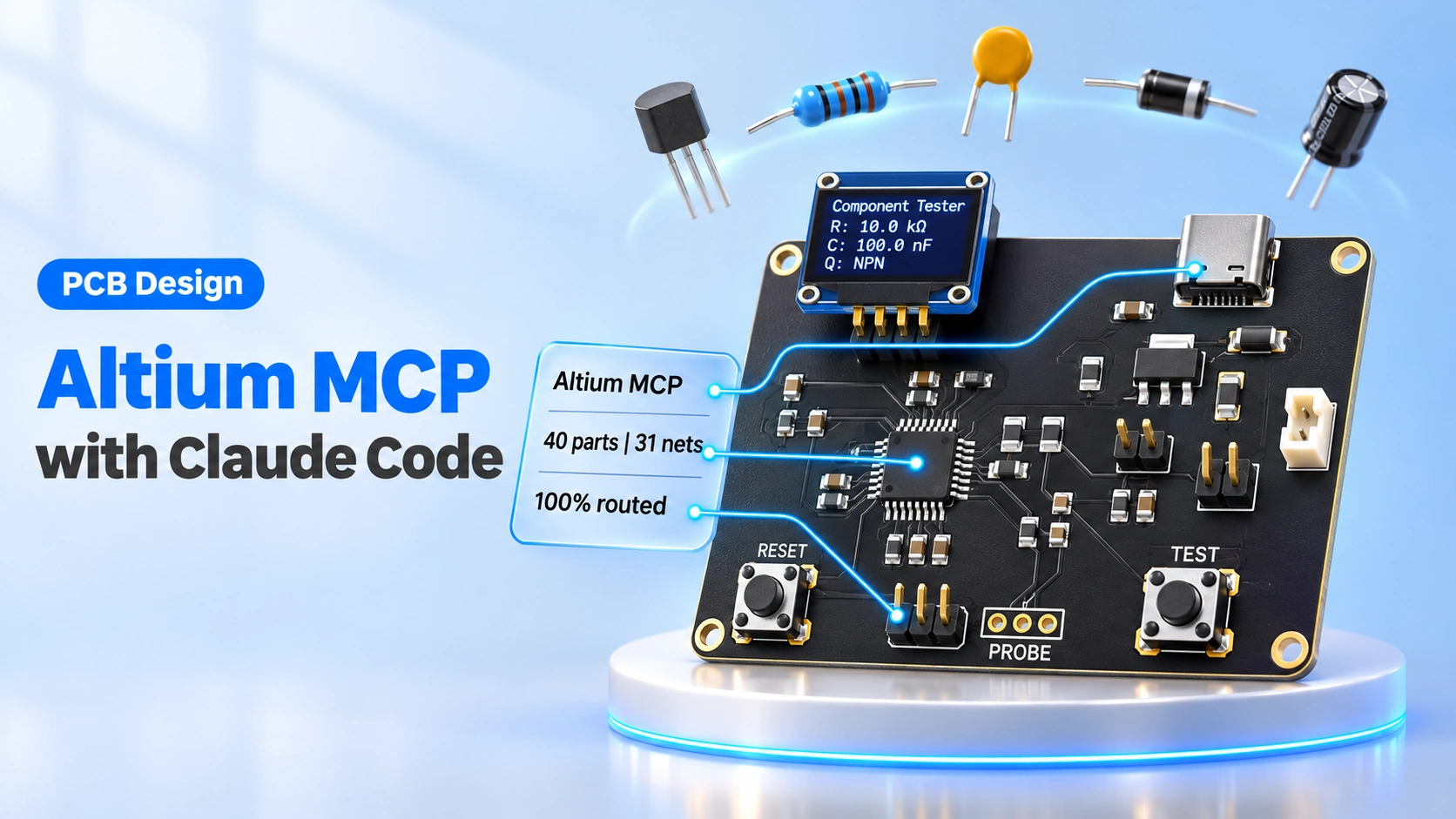
Introduction
Can Claude Code help design a PCB directly in Altium Designer? With an Altium MCP server, it can access a live project, create and modify design elements, and execute tasks through tool calls. But how much of the PCB design process can it actually handle?
To find out, I used eda-agent, a third-party open-source MCP server, to rebuild my CH32V005 component tester as a 2-layer PCB. The project covers everything from component selection and schematic creation to footprint placement, routing, and design checks. This is a hands-on walkthrough of the workflow, including what Claude Code could automate and which engineering decisions remained under my control.
In this guide, you will learn:
- What an Altium MCP server is and how eda-agent works
- How to connect eda-agent to Claude Code and verify the setup
- How to build a PCB from component selection to a routed 2-layer board
- Where Claude Code needed corrections and human intervention
- How many tokens the workflow consumed and what its practical limitations were
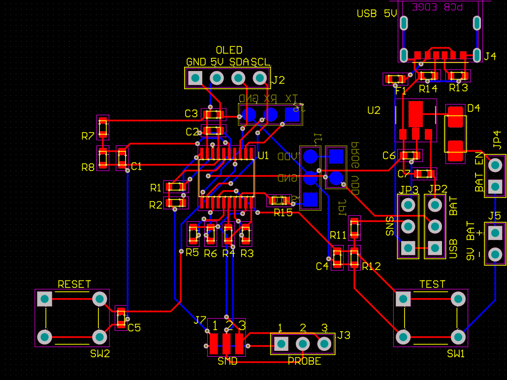
Figure: The CH32V005 component tester routed in Altium Designer through the Altium MCP server on a 60 x 45 mm 2-layer board.
Note
eda-agent is a third-party open-source project. Neither JLCPCB nor Altium develops, endorses, or supports it, and this article is for educational purposes only.
Before installing any repository, review its code, the data it shares, and what it can change. The author, JLCPCB, and Altium are not responsible for any damage to designs, files, or computers, or for information shared via the server.
What Is an Altium MCP Server?
An Altium MCP server is a bridge that exposes Altium Designer's scripting functions as tool calls an AI client can request. Claude Code requests an operation; the server runs it on the open design, and Altium returns the result as data.
MCP, the Model Context Protocol, is the open standard that Claude Code uses to communicate with these servers. Altium Designer does not run an AI model itself; the model behind Claude Code decides which tools to call.
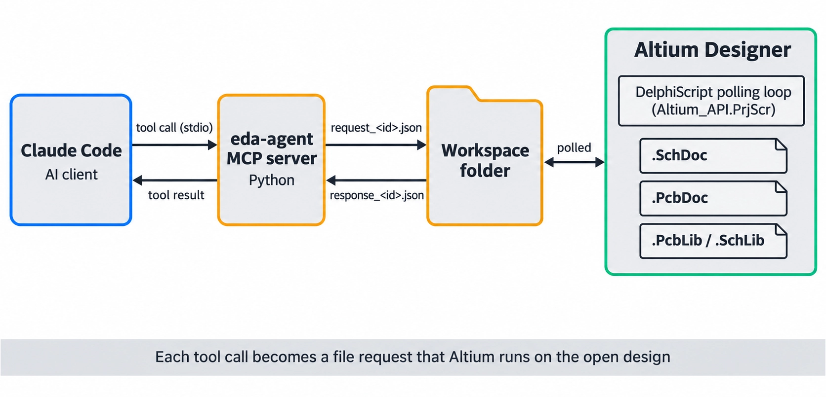
Figure: Altium MCP data path from Claude Code through the eda-agent server and its workspace files to the DelphiScript loop inside Altium Designer.
eda-agent wrote each tool call from Claude Code as a request file, running Claude Opus 5.5 for most of this build, and a DelphiScript loop inside Altium ran it and wrote the reply.
The Altium MCP Server Used in This Build
I used eda-agent 0.8.1 by George Saliba (salitronic), released under the Apache-2.0 license. It edits a live Altium session rather than exported files, and it covers libraries, schematics, and boards on a single server. Its author marks it experimental and notes that some tools can crash Altium's DelphiScript engine, so use it on a backed-up project. The same approach works in KiCad, as shown in this KiCad MCP guide.
Altium MCP Capabilities: Tool Groups and Safety Switches
eda-agent registers several hundred tools, grouped by the document they act on. In its minimal toolset, Claude Code sees two meta-tools, tool_catalog to search and tool_invoke to run, and reaches the other tools through them.
| Tool Prefix | Acts On | Used in This Build For |
|---|---|---|
| lib_ | .SchLib and .PcbLib libraries | Symbols, footprints, and footprint links |
| sch_ | The open .SchDoc | Drawing sheets from templates |
| pcb_ | The open .PcbDoc | Placement and routing |
| obj_ | Schematic or board objects | Tenting vias, edits, and deletes |
| proj_ | The project | Compiling, nets, and ERC |
| app_ | Altium itself | Saving and switching documents |
Four safeguards limit what the server can do:
- EDA_AGENT_READONLY=1: Refuses every command that is not a read. I started in this mode.
- EDA_AGENT_UI_AUTOMATION=0: Refuses synthesized keyboard and mouse input, so the server cannot click through Altium dialogs.
- Script block: Even in write mode, the server refuses to run Altium's script processes.
- EDA_AGENT_UPDATE_CHECK=0: Stops the daily update check from reaching the network.
How to Set Up the Altium MCP Server with Claude Code
Setup has four parts: install the eda-agent in a Python environment, load its project script in Altium, start the polling loop, and register the server with Claude Code. Start in read-only mode and enable write access when you need it.
The easy way: Give Claude the repo link or screenshots of these lines, and tell Claude to install and set up the environment for your user.
1. Install eda-agent in a Python 3.11 or newer virtual environment, then copy its Altium scripts:
|
|---|
2. Register the script project in Altium once: Preferences > Scripting System > Global Projects > Install from file, then select Altium_API.PrjScr.
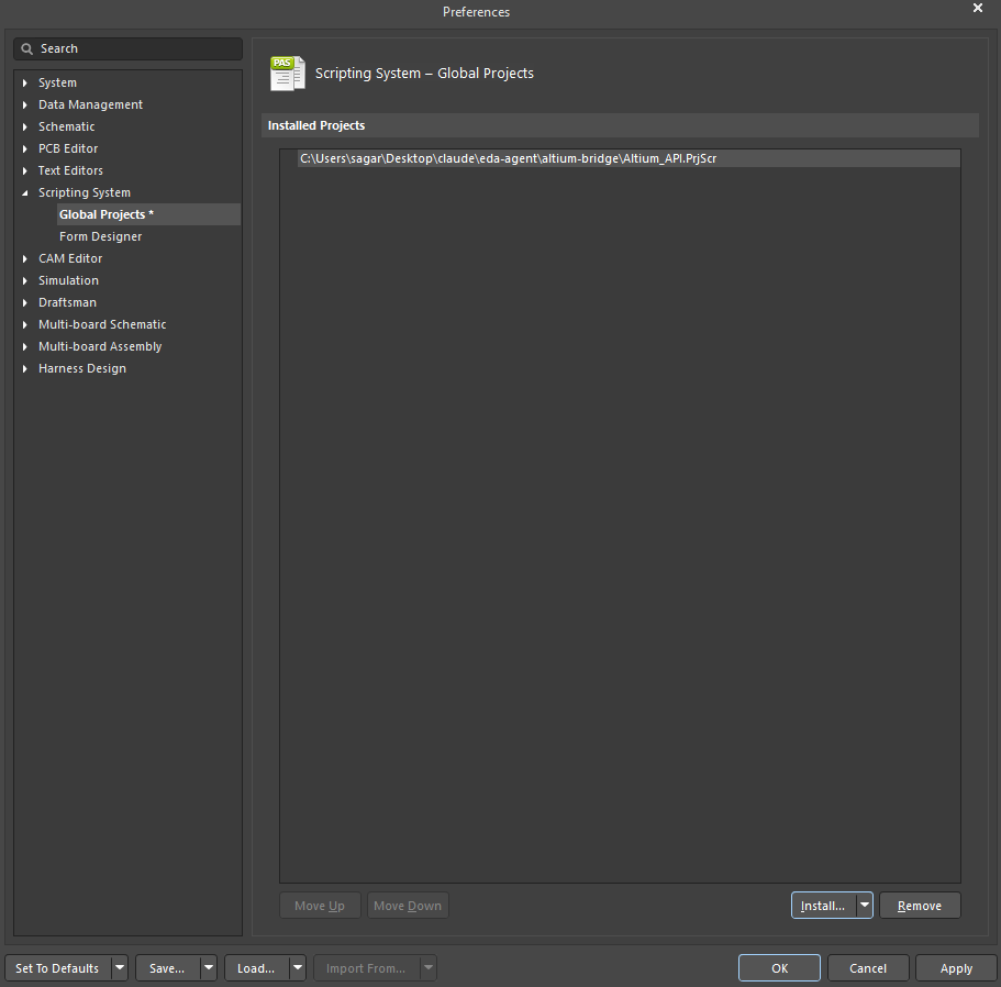
Figure: Altium Preferences showing the eda-agent Altium_API.PrjScr script project under Global Projects.
3. Start the polling loop: File > Run Script, expand Altium_API and Dispatcher.pas, select StartMCPServer, and click OK.
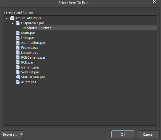
Figure: StartMCPServer selected in Altium Designer's Run Script dialog to start the Altium MCP polling loop.
4. Register the server with Claude Code in read-only mode. Run this command yourself, because in my setup Claude Code was not permitted to change its own MCP configuration:
|
|---|
5. Restart Claude Code. The Altium tools load only in a new session.
6. Enable write access when ready: run claude mcp remove altium --scope user, repeat the add command with EDA_AGENT_READONLY=0, and restart Claude Code again.
The --headless flag skips the eda-agent web dashboard; the status window in Altium still runs.
The Altium MCP Test Project: A CH32V005 Component Tester
The test board is a component tester that can identify and measure common electronic components. You connect a part to its three probes, and the firmware identifies and measures it: transistors, MOSFETs, diodes, thyristors, resistors, capacitors, or inductors.
Many transistor tester designs are available, and several build on a single open-source AVR project. I had already written my own RISC-V firmware for WCH CH32V chips, so the next job was a PCB. My version extends the AVR design to CH32V MCUs.
The project builds on:
- AVR Transistortester: the original design by Markus Frejek, carried on by Karl-Heinz Kübbeler, on the mikrocontroller.net AVR Transistortester page.
- Source code and manuals: the transistortester repository, with the firmware, hardware files, and documentation.
- ArduTester V1.13: plouc68000's Arduino Uno port, on Arduino Project Hub.
My firmware reimplements those measurement methods for RISC-V rather than translating the AVR code. It builds at 19,448 bytes of flash and 732 bytes of RAM, and it has not been bench-tested yet.
Step 1: Choosing Components for the Altium MCP Build
I asked Claude Code to choose the parts, starting with the MCU. It checked six candidates against live JLCPCB stock and recommended the CH32V005F6P6 because it was in stock and pin-identical to the original chip.
Why Claude Code Chose the CH32V005F6P6 MCU
| MCU | JLCPCB Stock on 2026-11-03 | Board Change Needed |
|---|---|---|
| CH32V006F8P6 (original) | 0 | None, but it could not be bought |
| CH32V005F6P6 (C54824605) | 195 | None, pin-identical in TSSOP-20 |
| CH32V007 | 0 | New package |
| CH32V003F4P6 | 25,148 | None, but 16 KB of flash cannot hold the 19,448-byte firmware |
| PY32F030F18P6 | 379 | New pinout and a firmware port |
| ATmega328P-AU | 35,775 | Full redesign |
What the CH32V005F6P6 brings to the tester:
- Core and memory: A 32-bit QingKe RISC-V2C core at up to 48 MHz, with 32 KB of flash and 6 KB of SRAM.
- 5 V operation: Rated from 2.0 to 5.5 V, or 2.4 to 5.5 V with the ADC running, so it runs at 5 V like the AVR original.
- ADC: 12-bit, with sampling above 1 Msps at a 4.5 to 5.5 V supply.
- Comparator timing: The op-amp output on PD4 is also the TIM2_CH1 capture input, so the AVR tester's comparator timing method carries over.
Claude recommended the change from the stock data and the WCH datasheet, and I approved it.
Other Components on the Tester BOM
For the rest of the board, Claude kept the proven tester values and checked each part against JLCPCB stock.
| Reference | MFR.Part # | JLCPCB Part# | Role |
|---|---|---|---|
| U2 | MCP1702-5002E/MB, SOT-89 | C18299 | 9 V to 5 V LDO, 2 µA typical quiescent current |
| D4 | SS14 Schottky, SMA | C2480 | Battery reverse-polarity protection |
| J4 | SHOU HAN 6-pin USB-C | C456012 | Power-only USB input |
| F1 | SMD0603P025TF | C20786 | 250 mA PTC fuse on USB |
| R1 to R6 | 680 Ω and 470 kΩ 1%, 0603 | C23228, C23178 | Probe resistors |
| C3, C6 | 10 µF 25 V, 0603 | C96446 | Bulk capacitors |
| SW1, SW2 | HRO K2-1102DP-C4SW-04 | C110153 | 6 x 6 mm through-hole tact switches |
Claude also checked the USB-C footprint against the manufacturer's drawing and found the old footprint's pads longer and shifted back by 0.25 mm. Each buyable part carries a JLCPCB part number and MPN, which you can check in the JLCPCB Parts Library.
Step 2: Drawing the Altium Schematic Through the MCP
Claude Code drew 16 symbols and the schematic sheets through the MCP, then compared Altium's compiled netlist with a pin-to-net spec from the verified EasyEDA design. The first pass matched all 33 nets and 134 pins, with 0 ERC errors.
- Spec first: the verified pin-to-net list was added to build_spec.json, the reference for every netlist check.
- Symbols and sheets: symbols were created one per call, and sch_draw_template drew each sheet from a template, stopping before the first wire if the wiring would short two nets.
- Footprints: a 14-footprint library built from KiCad 10 dimensions, including custom USB-C, probe-pad, test-pad, and switch footprints.
Sheet 1: MCU Front End and Probe Network
Sheet 1 holds the MCU, the probe network, and the comparator threshold, where every tester measurement starts.
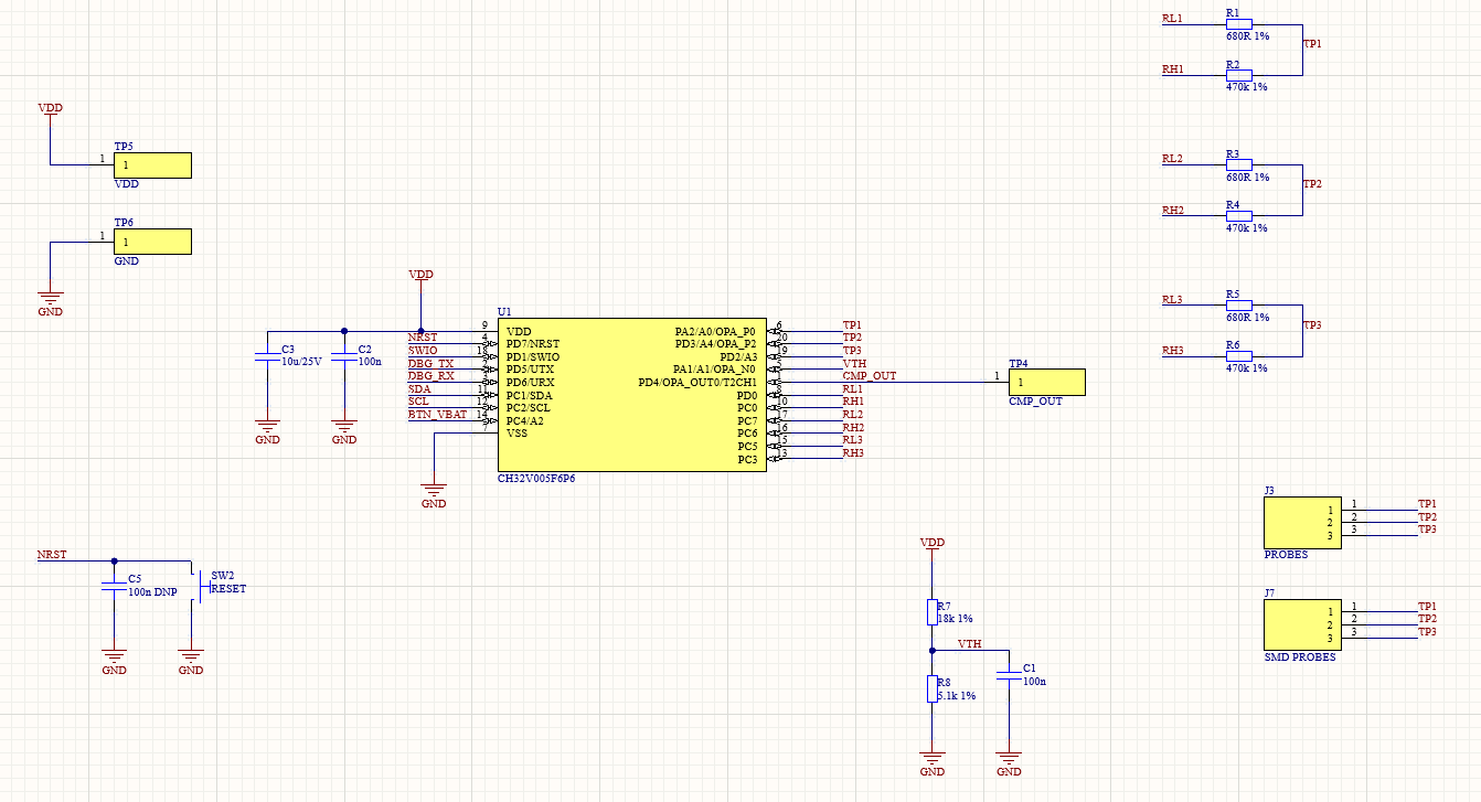
Figure: Sheet 1 of the Altium MCP schematic: the CH32V005F6P6, the 680 Ω and 470 kΩ probe resistors, the VTH divider, and the J3 and J7 probe connectors.
| MCU Pin | Net | Function |
|---|---|---|
| PA2, PD3, PD2 | TP1, TP2, TP3 | Probe ADC inputs; TP1 and TP2 also reach the comparator |
| PD0, PC7, PC5 | RL1 to RL3 | Probe drive through 680 Ω |
| PC0, PC6, PC3 | RH1 to RH3 | Probe drive through 470 kΩ |
| PA1 | VTH | Comparator threshold input |
| PD4 | CMP_OUT | Comparator output to TIM2 capture |
| PC4 | BTN_VBAT | Supply sense and TEST button |
| PC1, PC2 | SDA, SCL | OLED I2C bus |
| PD5, PD6 | DBG_TX, DBG_RX | UART debug |
| PD1, PD7 | SWIO, NRST | Programming and reset |
- VTH divider: R7 (18 kΩ) and R8 (5.1 kΩ) set the threshold at 0.2208 x VDD, about 1.10 V at 5 V. That recreates the AVR tester's 1.1 V-to-5 V ratio, so its lookup tables stay valid.
- Probe connectors: J3, a 3-pin header, and J7, three bare SMD pads, are wired in parallel for leaded and surface-mount parts.
- Support parts: C2 and C3 decouple VDD, SW2 resets the MCU (C5 is DNP), and TP4 to TP6 expose CMP_OUT, VDD, and GND.
Sheet 2: Power, USB-C, and Interfaces
Sheet 2 holds both power inputs, the power and sense selectors, and the interface headers.
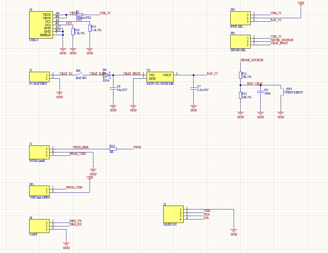
Figure: Sheet 2 of the Altium MCP schematic: the USB-C input, the 9 V battery path through the MCP1702 LDO, the PWR SEL and SENSE SEL jumpers, and the interface headers.
- USB-C input: R13 and R14 (5.1 kΩ) pull CC1 and CC2 to ground, thereby identifying the board as a power sink, and F1 supplies USB_5V.
- 9 V battery path: J5 feeds JP4 (BAT EN), D4, and the MCP1702 LDO to make BAT_5V. D4 blocks a reversed battery, and removing JP4 disconnects the battery completely.
- Power select: JP2 connects VDD to USB_5V on pins 1–2 or BAT_5V on pins 2–3; open means off.
- Sense select: JP3 routes USB_5V or VBAT_PROT to the sense divider and must match JP2, but nothing on the board enforces this.
- Sense and button: R11 (18 kΩ) and R12 (10 kΩ) scale the sensed voltage by 10/28, so 9 V appears as about 3.2 V at BTN_VBAT. SW1 pulls the same node low, so one ADC pin reads the supply and the TEST button.
- Headers: J1 is the WCH-LinkE header, with JP1 left open so the WCH-LinkE does not power VDD by default. J6 carries the UART, and J2 the OLED's I2C bus.
What Changed in the Schematic During Review
| Revision | Change | Parts, Nets |
|---|---|---|
| C2 | Slide switch replaced by two separate 1x3 jumpers (JP2, JP3), so a misplaced shunt cannot join 9 V to the 5 V rail | 48, 33 |
| C4 | JP4 battery jumper added | 52, 34 |
| C5 | I2C level shifter removed (Q1, Q2, R16, R17) | 48, 32 |
| C6 | R9 and R10 removed, since the OLED module has its own pull-ups; three sheets merged into two | 46, 32 |
| C8 | OLED moved to 5 V (U3, C8, C9 removed), BAV199 clamps D1 to D3 removed, switches changed to through-hole | 40, 31 |
Step 3: Placing the Components Through the Altium MCP
Claude Code made the first placement through the MCP. It had no overlaps, but its ratsnest crossed the whole board, so I placed every part by hand.
First Placement by Claude Code
pcb_place_components placed 46 parts on a 75 x 55 mm board, each carrying its schematic UniqueId and pad nets, so Altium treated the board as in sync without an ECO dialog. Claude proposed a 60 x 45 mm board. I approved it, and the parts moved with pcb_import_placement.
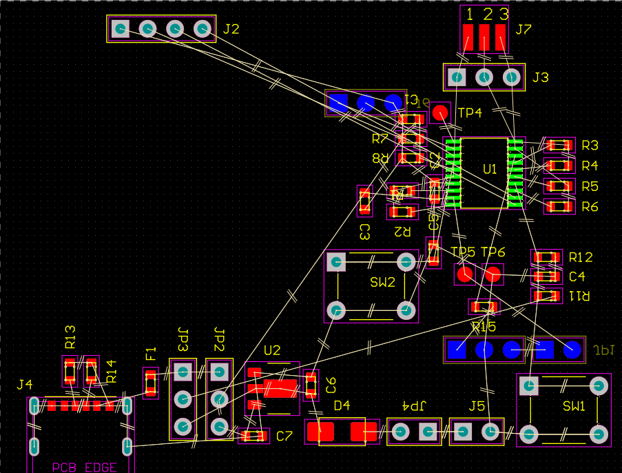
Figure: Claude Code's placement through the Altium MCP before hand placement.
Hand Placement and Silkscreen Clean-Up
I placed the USB-C connector on the top edge, the probe connectors on the bottom edge, the OLED header at the top, and the power jumpers beside the battery input. Claude read back my positions from the board before editing, so it didn't overwrite my layout.
- Bottom side: J1, J6, and JP1 moved to the bottom layer, later as bottom-only SMD header footprints. Since obj_modify cannot change a footprint, Claude deleted each part and placed it again at the same position, rotation, and UniqueId.
- Alignment: equivalent parts were aligned, such as R3-R6 evenly spaced and J7 in line with J3.
- Silkscreen labels: 28 net and function labels, such as probe numbers, OLED pins, and jumper positions.
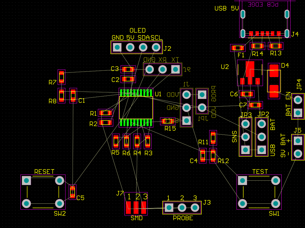
Figure: Hand placement of the tester on the 60 x 45 mm Altium MCP board.
Step 4: Autorouting the Board Through the Altium MCP
eda-agent's pcb_autoroute tool runs the server's own router, not Altium's Situs autorouter, against the board's design rules. With Altium's default rules, it reached 97.6%; with rules set inside JLCPCB's 2-layer capabilities, it reached 100%.
Altium Default Rules vs. Rules Set to JLCPCB Capabilities
| Rule | Altium Default | Value Used | JLCPCB 2-Layer Minimum |
|---|---|---|---|
| Clearance | 10 mil | 0.20 mm | 0.10 mm |
| Via diameter and hole | 50 and 28 mil | 24 and 12 mil (0.61 and 0.30 mm) | 0.25 and 0.15 mm |
| Solder mask sliver | 10 mil | 4 mil (0.10 mm) | 0.10 mm bridge, green, 1 oz |
| Track width | 10 mil | 10 mil | 0.10 mm |
Every adjusted value meets JLCPCB's minimum, and the clearance and via sizes keep a margin above it. General PCB routing rules cover width and spacing beyond this board.
| Result | Run 1: Default Rules | Run 2: Adjusted Rules |
|---|---|---|
| Completion | 97.6% | 100% |
| Unrouted nets | 2 (RL2, RL3) | 0 |
| Tracks at 10 mil | 269 | 270 |
| Vias, and vias in pads | 37, with 7 in pads | 48, with 0 in pads |
| Clearance flags | 18, all U1 pad pairs | 0 |
| Mask-sliver flags | 31 | 14 |
| Applied to the board | No | Yes |
Run 1 failed at the MCU: RL2 and RL3 could not reach U1, and all 18 clearance flags are U1's own pads, 9.84 mil apart at 0.65 mm pitch, inside the 10 mil default clearance. Run 2 was applied with 270 tracks, 48 vias, and no copper pour.
Altium DRC Results After Routing
Altium's design rule check found 0 copper violations
| DRC Rule | Violations |
|---|---|
| Clearance, short-circuit, unrouted net, width, hole | 0 |
| Minimum solder mask sliver, 4 mil | 0 |
| Silk to solder mask, 10 mil | 0 |
| Silk to silk, 10 mil | 0 |
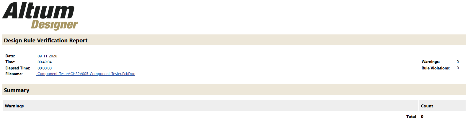
Figure: Altium DRC summary for the Altium MCP-routed tester
Step 5: Altium MCP Output Files and Design Documents
The MCP build produced the Altium project, its libraries, a verification spec, and review reports. Gerber, drill, BOM, and pick-and-place files have not yet been generated, and the board has not been ordered.
| File | What It Contains |
|---|---|
| .PrjPcb project and twoSchDoc sheets | The Altium project and schematic |
| .PcbDoc | The routed 60 x 45 mm board |
| .SchLib and .PcbLib | 16 symbols; 14 footprints plus 2 bottom-side SMD headers |
| build_spec.json | The pin-to-net spec for netlist comparison |
| DRC report and autoroute job results | Rule check and both router runs |
| Schematic PDF | A print of both sheets |
Outputs Still Needed for a JLCPCB Order
- Open items: 1.0 mm silkscreen text, the TP4-to-TP6 decision, a ground pour, power-net track widths, via tenting and mask slivers, and three designator rotations.
- Gerber and drill files: export them using this guide on how to generate Gerber files in Altium Designer.
- BOM and pick-and-place: export both from the JLCPCB numbers already on the parts for PCB assembly.
- DFM review: upload the Gerbers to JLCDFM and check the mask slivers there.
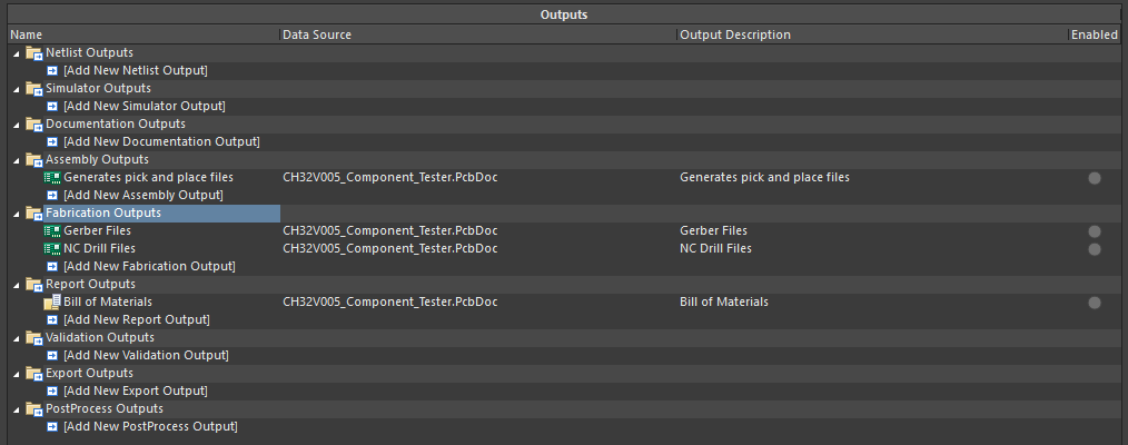
Figure: Output Job setup in Altium Designer for the CH32V005 tester, ready to generate the Gerber, drill, BOM, and pick-and-place files for a JLCPCB order.
Altium MCP Accuracy: Where Human Review Was Needed
The Altium MCP output was fast but not self-checking. Most errors surfaced in a compile, an ERC run, or a read-back of the board, and the engineering decisions still needed a person.
Altium MCP Errors and Tool Limits in This Build
| Problem | Fix |
|---|---|
| Bulk symbol creation put every pin on the last symbol | One symbol per call, with a pin-count check |
| Claude's edit to a sheet-generator script commented out two net labels | Caught by compile and ERC; labels restored |
| A sheet redraw re-issued four UniqueIds | Four board parts placed again with the new IDs |
| U1 drifted up to 0.5 mm after delete-and-place edits | Moved back; positions now read back after each edit |
| A PCB query read another open board | The board is now focused before each query |
| obj_modify cannot change a footprint or text rotation | Parts placed again; three rotations left for manual fixing |
| The pcb_autoroute call hung for about 30 minutes after the job finished | Result recovered from the job status |
Design Decisions the Engineer Made
- Approving the CH32V005F6P6 and the 60 x 45 mm board size
- Two separate jumpers instead of a slide switch
- Removing the level shifter and the probe clamps, and running the OLED on 5 V
- Placing every part, moving J1, J6, and JP1 to the bottom, and approving every delete
Where AI Saves Prototype Time in an Altium MCP Build
AI can shorten the time to a prototype by producing repetitive design files faster than drawing them by hand.
- Libraries and sheets: the first 16 symbols and three schematic sheets took about 17 minutes, and the 14-footprint library about 9 minutes.
- Component search: Claude compared six MCUs against live JLCPCB stock and found a pin-identical alternative, a stock-checked comparison that a general web search does not return in one step.
- Repeat checks: ERC, netlist comparisons, and DRC summaries ran after each change.
In this build, though, every stage of the PCB design still needed human input.
Altium MCP Token Usage: Models and Tool Calls by Session
The build ran across two Claude Code sessions and processed about 186 million tokens. About 98% were cache reads, because each reply re-reads the whole conversation. Session 2 switched models with /model.
| Item | Session 1 | Session 2 | Total |
|---|---|---|---|
| Work covered | Schematic to hand placement | Footprints, routing, DRC | Full build |
| Model | Claude Opus 5.5 | Claude Opus 5.5 (49 replies), Claude Sonnet 5.5 (45) | Mixed |
| Assistant replies | 365 | 96 | 461 |
| All tool calls | 536 | 109 | 645 |
| Altium MCP tool calls | 340 | 84 | 424 |
| Output tokens | 345,679 | 39,036 | 384,715 |
| Input, uncached | 800 | 202 | 1,002 |
| Input written to cache | 2,386,008 | 664,051 | 3,050,059 |
| Input read from cache | 165,279,616 | 17,456,267 | 182,735,883 |
| Total processed | 168,012,103 | 18,159,556 | 186,171,659 |
- What raised the count: large inline tool results, such as placement payloads, netlists, and a 207-entry DRC list, plus the redraws after the bulk-symbol error.
- How to reduce it: save large results to a file and summarize them with a script, as was done for the DRC report.
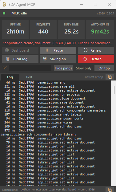
Figure: The EDA Agent status window in Altium Designer logging Altium MCP requests: 440 requests in 2 h 10 min of uptime, each with its duration.
Conclusion
An Altium MCP server makes Claude Code a fast CAD operator inside Altium Designer, not an autonomous PCB designer. Use Claude Code for stock-checked part searches and the server for symbols, footprints, schematic entry, and routing runs, and keep the circuit decisions, placement, and final review with the engineer.
With that split, the CH32V005 tester went from component selection to a routed 2-layer board in two sessions. Review any third-party MCP server before you install it.
Once your PCB design is finalized and passes the necessary DFM checks, export your Gerber files and upload them to JLCPCB to get an instant fabrication quote.
Turn your AI-assisted PCB design into a physical board.
FAQs About Altium MCP
Can an Altium MCP Server Design a PCB on Its Own?
No. In this build, Claude Code drew the schematic, placed parts, and routed the board, but the engineer made the circuit decisions, the final placement, and approved every delete.
Does an Altium MCP Server Send My Design Data to the AI?
Yes. Anything the server reads, such as part values, net names, and parameters, enters the Claude Code conversation and is processed by the AI provider. Check this before opening confidential designs.
Does the Altium MCP Server Use Altium's Own Autorouter?
No. eda-agent's pcb_autoroute runs the server's in-house router against the board's design rules, and it writes tracks and vias only after the job is applied.
Which Altium Designer Version Works with This MCP Server?
Altium Designer 20 or later is preferred, according to the eda-agent README, with Python 3.11 or newer. This build used Altium Designer 26.11.1.5 and eda-agent 0.8.1.
Can an Altium MCP Board Go Straight to Fabrication?
No. This board still needs Gerber, drill, BOM, and pick-and-place files, 1.0 mm silkscreen text, and a DFM review of its mask slivers before ordering.
Popular Articles
• GPT-6 Astra PCB Design in EasyEDA Pro: What Worked, What Failed, and What We Learned
• Altium MCP with Claude Code: From Setup to PCB Design
• KiCad MCP: How to Design a PCB with Claude Code [Step-by-Step]
• Altium MCP: AI PCB Design with GPT-6 and Codex [Step-by-Step Guide]
• AI PCB Design: From Prompt to PCB with EasyEDA Pro
Keep Learning
Choosing the Right PCB Shape
key takeaway Choose a PCB shape based on layout, space, and application requirements. Consider edge clearance, cutouts, and manufacturing feasibility early. Select suitable routing and panelization methods for reliable production. Work with JLCPCB to turn custom PCB designs into manufacturable products. Selecting the right PCB shape is an important part of electronic product design. Beyond determining how a circuit board fits inside an enclosure, its geometry also affects component placement, signal r......
Designing Durable Custom Keyboard PCBs: Tailored Solutions and Expert Fabrication
So what's a keyboard PCB? In simple terms, it is the printed circuit board that is contained in the center of any keyboard, connecting the key switches to the controller, which communicates with your computer. Hitting a key closes a circuit on the PCB, which the controller records what key it was and transmits that keycode back to your host device. The mechanical-keyboard community is a subculture that has developed out of a niche hobby to become a successful subculture in the mechanical-keyboard worl......
GPT-6 Astra PCB Design in EasyEDA Pro: What Worked, What Failed, and What We Learned
Key Takeaways What was tested: GPT-6 Astra was given access to a native EasyEDA Pro 3.2.149 installation and asked to design a stereo TPA3116D2 amplifier from a four-line written brief. What it produced: The run resulted in a 44 × 34 mm, two-layer PCB with 40 SMD components and an editable native EasyEDA Pro project with embedded libraries. Where it failed: The first complete import opened cleanly and looked plausible, yet the initial native verification reported 50 association mismatches involving 12......
Claude Code PCB Design: Can It Build a Real Board in EasyEDA Pro?
Key Takeaways Claude Code PCB design: Using Claude Opus 5.5 and EasyEDA Pro 3.2.149, I converted a 47-component, three-page schematic from a PDF into a fully routed, two-layer PCB with zero DRC errors. EasyEDA Pro integration: The EasyEDA API skill connects Claude Code to EasyEDA Pro through a local bridge server and the Run API Gateway extension. This allows Claude to control the editor via JavaScript, with a 30-second timeout per API call. Design verification: A successful API response doesn't alway......
Guide to PCB Via Design: Best Practices, Tips, and Key Considerations
High-quality PCB design not only requires innovative concepts but also relies on a deep understanding of PCB manufacturing processes. Via design, as one of the critical steps in PCB design, is crucial for both PCB performance and manufacturing efficiency. Can vias be designed in any size? To answer this question, let’s first understand how holes on a PCB are created. 1. Cutting the Material: PCB manufacturers use automatic cutting machines to slice large copper-clad laminates into substrates of specif......
AI PCB Design: From Prompt to PCB with EasyEDA Pro
Key Takeaways AI PCB design uses AI agents to automate schematic creation, component selection, layout, and verification inside a real EDA editor — not just generate images. The workflow connects EasyEDA Pro to an AI coding agent (Claude Code or Codex) through the EasyEDA API Gateway, the open-source API Skill, and a local bridge server. Setup takes about ten minutes and is fully local-first: designs, API calls, and intermediate code never leave your machine. Because the agent places real library part......