Claude Code PCB Design: Can It Build a Real Board in EasyEDA Pro?
15 min
- Claude Code PCB Design Results: What the AI Built
- How Claude Code Controls EasyEDA Pro Through the API Skill
- How to Connect Claude Code to EasyEDA Pro From GitHub
- Building a Multi-Page Schematic From a PDF With Claude Code
- Making a Schematic JLCPCB Assembly-Ready With Live Stock Checks
- EasyEDA Pro 3.2.149 API Issues and Fixes
- PCB Component Placement with Claude Code
- Autorouting an EasyEDA Pro Board With Freerouting
- What Claude Code Cannot Do in PCB Design Yet
- Conclusion
- FAQs About Claude Code PCB Design
Key Takeaways
- Claude Code PCB design: Using Claude Opus 5.5 and EasyEDA Pro 3.2.149, I converted a 47-component, three-page schematic from a PDF into a fully routed, two-layer PCB with zero DRC errors.
- EasyEDA Pro integration: The EasyEDA API skill connects Claude Code to EasyEDA Pro through a local bridge server and the Run API Gateway extension. This allows Claude to control the editor via JavaScript, with a 30-second timeout per API call.
- Design verification: A successful API response doesn't always mean the design is correct. By reading back and checking the netlist, I verified all 138 pin connections across 33 nets and identified six missing GND connections that needed fixing.
- PCB routing: EasyEDA Pro 3.2.149 doesn't provide an autorouter through its API, so I used Freerouting in single-threaded mode. The vias were imported first, followed by the tracks, to complete the routing.
- Manual review: Claude Code worked with coordinates and API data rather than directly viewing the board. Visual inspection, mechanical clearance checks, thermal considerations, and final component selection still required human review.
I designed a working PCB using Claude Code and EasyEDA Pro, with AI handling everything from schematic creation to PCB routing. I used Claude Opus 5.5 and the official EasyEDA API skill to connect Claude Code with EasyEDA Pro, allowing Claude to interact directly with the PCB design software.
In this article, I'll walk through the complete process, from setting up the API connection and integrating EasyEDA Pro with Claude Code. It rebuilt the three-sheet schematic of my CH32V006 component tester from a PDF, swapped out-of-stock parts, and routed a two-layer board to a clean DRC.
However, the process wasn't entirely smooth. Some component attributes were lost without warning, the API bridge timed out, and the autorouter was missing. Each issue required a workaround, which I'll also cover so you know what to expect when trying this yourself.
In this case study, you will learn:
- How to connect Claude Code to EasyEDA Pro from GitHub
- How to rebuild and verify a schematic from a PDF
- How to route the board with Freerouting
- Which steps still need a human engineer
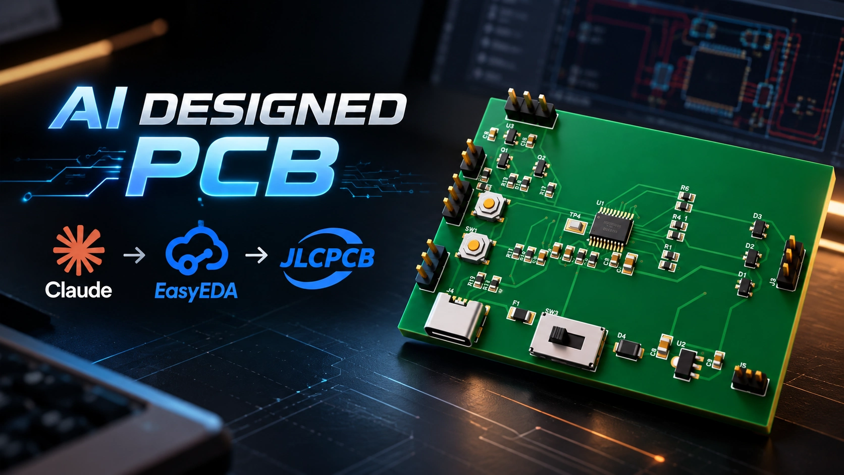
Figure: Claude Code PCB design result: the routed CH32V006 tester PCB
Claude Code PCB Design Results: What the AI Built
Claude Code, running Claude Opus 5.5, took a real 47-part design from a design specification document, and routed a two-layer PCB with zero DRC errors. I handled project creation, dialog approvals, and every sourcing decision.
The board is my CH32V006 three-probe component tester, a port of the AVR-based ArduTester to a WCH RISC-V microcontroller.
| Task | Done by Claude Code | Human Step | Result |
|---|---|---|---|
| Setup | Installed the skill, started the bridge, ran the first API call | Enabled Allow External Interaction | Live link to EasyEDA Pro 3.2.149 |
| Schematic | Placed 47 parts (27 unique LCSC devices) on 3 pages | Created the empty project | Every part is an LCSC library part with a footprint |
| Netlist check | Read back pins, wires, and labels, then compared them with the PDF | Reviewed the report | 138/138 pins, 33 nets, no shorts |
| Stock swaps | Checked JLCPCB stock and proposed replacements | Approved each swap and kept the MCU | 8 part changes |
| Placement | Placed all footprints from the written zone rules | Clicked Apply on the import dialog | 71.1 × 50.8 mm, 2 layers, no pad collisions |
| Routing | Ran Freerouting and imported the routes | None | 443 segments, 28 vias, 33/33 nets connected |
| DRC | Fixed reported errors and rebuilt the pours | Pasted the DRC log into the session | Schematic: 0 errors, 0 warnings; PCB: 0 errors |
How Claude Code Controls EasyEDA Pro Through the API Skill
Claude Code controls EasyEDA Pro by writing JavaScript that runs inside the open editor, is sent through a local bridge server, and is processed by the Run API Gateway extension. It edits the live design rather than generating circuit images.
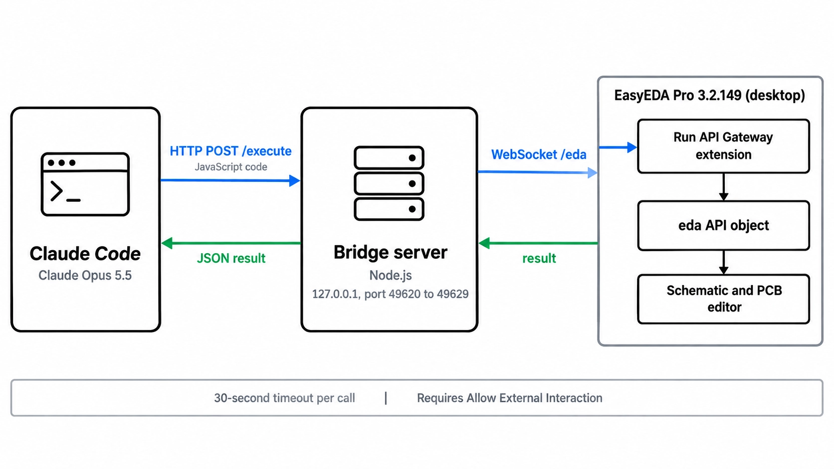
Figure: Claude Code sends JavaScript to the bridge, which relays it to the Run API Gateway extension inside EasyEDA Pro
The EasyEDA API skill gives Claude Code three things:
- API reference: About 120 classes, 62 enums, and 70 interfaces, so the model looks up real method signatures instead of guessing them.
- Bridge server: A Node.js server that runs locally on your computer and connects Claude Code to EasyEDA Pro. It uses the local IP address 127.0.0.1 and automatically selects an available port between 49620 and 49629.
- SKILL.md instructions: How to find the bridge, select an EasyEDA window, and send code.
How to Connect Claude Code to EasyEDA Pro From GitHub
Setup takes six steps:
1. Download the EasyEDA API skill.
2. Install the required dependency.
3. Register the skill with Claude Code.
4. Install the extension in EasyEDA Pro.
5. Start the local bridge server.
6. Run a test command to verify that Claude Code and EasyEDA Pro are connected and working correctly.
The AI PCB design guide for EasyEDA Pro covers prompting in more depth.
My setup used:
- Windows 11 and the EasyEDA Pro 3.2.149 desktop client in local mode
- Node.js 24 (the skill requires version 18 or later)
- Claude Code with Claude Opus 5.5
- Java 21, needed only for the Freerouting step
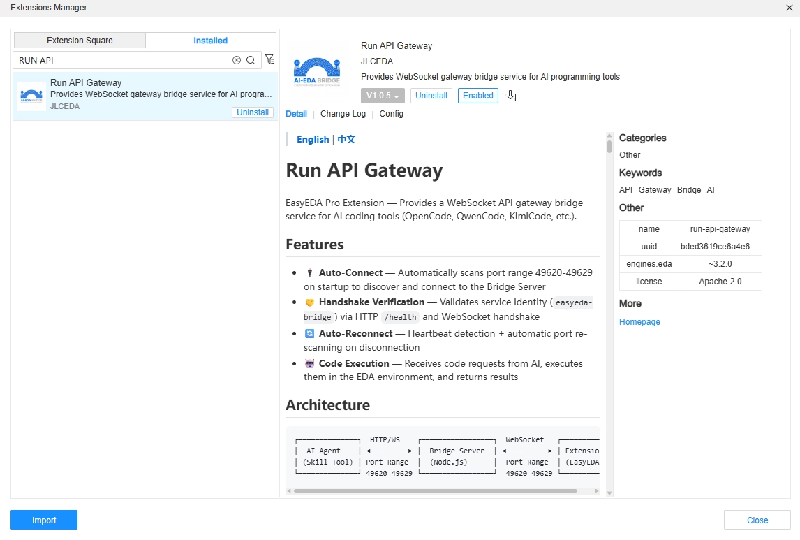
Figure: EasyEDA Run API Gateway Extension
Install the extension (Run API Gateway) from the extension manager under EasyEDA advanced settings.
The setup sequence: (copy and paste this sequence; in Claude, it will automatically set up all the things for you)
1. Download the skill from GitHub and unzip it.
2. Run npm install in the skill folder. The only dependency is the ws WebSocket package.
3. Register the skill with Claude Code. On Windows, I created a directory junction from Command Prompt (cmd.exe), because mklink is not a PowerShell command:
|
|---|
4. Install run-api-gateway_v1.0.6.eext in EasyEDA Pro from the Run API Gateway extension page.
5. Start the bridge as a standalone process in PowerShell:
|
|---|
6. Send the first test call from a Bash shell (Git Bash or WSL on Windows), using the port the bridge printed at start-up:
|
|---|
The easy method: Give this setup sequence to Claude, grant all required permissions, and it will automatically set it up for you. For more info, you can watch this video: AI Designed This PCB in 2 Hours.
Fixing "Bridge Not Found": Allow External Interaction
If the extension never connects, check its permission first. Without Allow External Interaction enabled in the Extension Manager, the extension's sys_WebSocket.The register call is blocked with no error message.
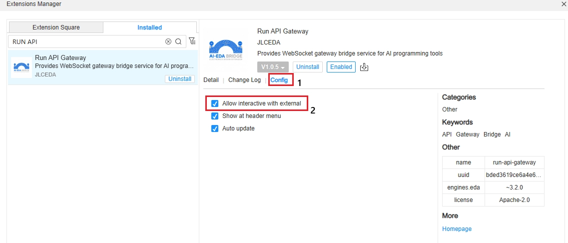
Figure: EasyEDA Pro Extension Manager with Allow External Interaction enabled for Run API Gateway
After enabling it, use API Gateway → Reconnect. The extension stops retrying after five failed attempts, so a bridge that starts later needs a manual reconnection.
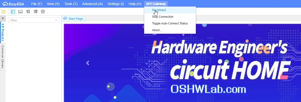
Figure: API Gateway Reconnect menu in EasyEDA Pro
Building a Multi-Page Schematic From a PDF With Claude Code
I provided Claude Code with the original three-page KiCad schematic as a PDF, along with the design specifications and a detailed pin map (CONNECTIONS.md). The CONNECTIONS.md file lists each microcontroller pin, its connected net, and the reason for that assignment. Based on this information, Claude Code organized the design into three schematic pages:
- MCU and Front End: Microcontroller and component measurement circuitry.
- Power and Interfaces: Power supply and external connections.
- OLED Interface: Display connections and supporting circuitry.
The process involved four main challenges: selecting the right components from the JLCPCB library, positioning them correctly, generating schematic pages, and handling API timeouts during the design process.
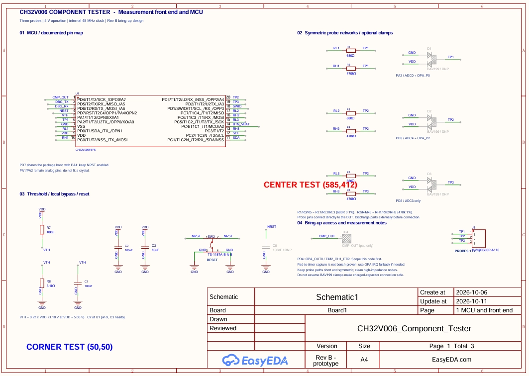
Figure: EasyEDA Pro schematic first page
- Resolving Every Part to an LCSC Library Device: Claude Code resolved each part using lib_Device.getByLcscIds, so every symbol had a real footprint. It then placed each device once, read back its real pin positions, and deleted it, so later wires could land exactly on the pins.
- Learning the EasyEDA Schematic Coordinate System: The schematic API uses 10-mil units, with y increasing upward. The A4 frame spans 0 to 1170 units horizontally and 0 to 825 units vertically.
- Generating Pages From a Written Spec: Claude Code drew each page using power symbols, short labeled wire stubs, and global net names instead of long wires. Each connection stays local to its pin, which keeps it easy to verify.
Making a Schematic JLCPCB Assembly-Ready With Live Stock Checks
Using the connections.md references, Claude Code selected suitable components from the JLCPCB Parts Library. Claude Code checked JLCPCB stock for every part and proposed in-stock replacements, preferring Basic parts.
I reviewed and approved each suggested replacement to make sure it matched the original design requirements. Even components with similar specifications can differ in pinout, voltage ratings, tolerances, or electrical behavior, so every substitution needs to be checked before the schematic is finalized.
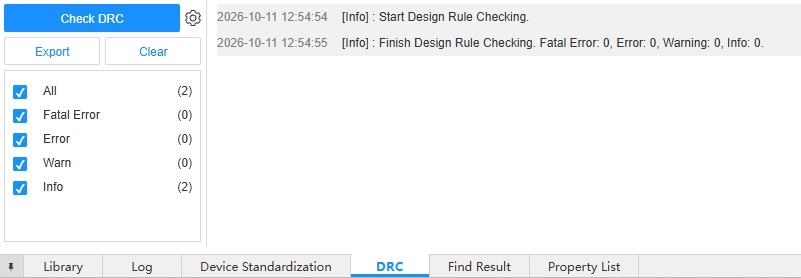
Figure: EasyEDA Pro schematic DRC reporting 0 errors and 0 warnings
Each part's type, Basic or Extended, is shown in the JLCPCB Parts Library; see how to identify Basic and Extended parts before you upload a BOM.
| Original Part | Replacement | LCSC Part | Library Type | Reason |
|---|---|---|---|---|
| 680 Ω 0.1% (R1, R3, R5) | 680 Ω 1% | C23228 | Basic | In stock; slightly lower accuracy on low-resistance and ESR readings |
| 39k / 11k divider (R7, R8) | 18k / 5.1k | C25810 / C23186 | Basic | Threshold ratio 0.2208 vs. 0.220 |
| 0466.250NR fuse (F1) | SMD1206P025TF 0.25 A PTC | C20798 | Extended | 0.25 A hold current, resettable; it trips at a higher current and more slowly than the fast-acting fuse |
| 2.2 µF 25 V (C6) | 10 µF 25 V 0805 | C15850 | Basic | Basic part at the same voltage rating |
| MCP1700 (U3) | XC6206P332MR | C5446 | Basic | Same SOT-23 pinout |
| BSS138 (Q1, Q2) | 2N7002 | C8545 | Basic | Works with the 3.3 V gate at 100 kHz I2C |
| C&K 7203SYCGE toggle (SW3) | SS-23D07-G050 slide | C54305660 | Extended | Original toggle at 0 stock |
| Keystone 5015 test point (TP4) | Bare pad | Not in BOM | None | Nothing to source |
EasyEDA Pro 3.2.149 API Issues and Fixes
Seven API problems in EasyEDA Pro 3.2.149 shaped this build. Several returned success while leaving the design wrong, so read-back checks were the reliable way to detect them.
| Symptom | Cause | Fix |
|---|---|---|
| Supplier Part reads "0603WAF4701T5E.1," and EasyEDA warns that component attributes do not match the supplier part | Parts placed through the API lose their attributes | One full modification () that sets supplier ID, MPN, manufacturer, name, and other properties together |
| The warning returns after a later edit | A name-only modify() breaks the attributes again | Rewrite all attributes in the same call every time |
| "Wire has multiple net names" | Two different net labels on one connected wire | Keep one net name per wire |
| Netlist export hangs | The export call never returns | Build the netlist from read-back data, as the verifier does |
| DRC returns counts only | The API reports totals, not error locations | Paste the DRC log from the editor into the session |
The GPT-6 Astra EasyEDA Pro review took a different approach to the same editor: it imported files rather than using the live API.
PCB Component Placement with Claude Code
Claude Code placed all 47 footprints from the written zone rules, then checked pad clearances with a script. EasyEDA's importChanges() call waits for a human to click Apply, so placement begins with a single manual step.
The zone rules came from the layout notes in CONNECTIONS.md:
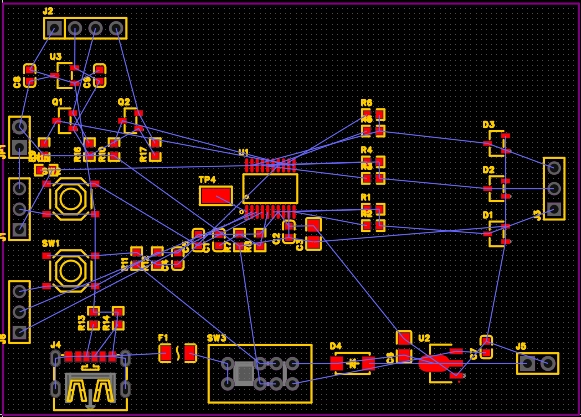
Figure: Placed the tester board with the probe, power, programming, and display zones
- Probe header (J3): On the right edge, to keep the three probe traces short.
- Threshold divider (R7, R8, C1): Tight to the MCU pin 5, away from the probe drivers.
- Power section: USB-C, battery header, regulators, and switch along the bottom edge.
- Programming header (J1): On the left edge.
- OLED header (J2): At the top left.
A scripted check then compared every pad pair and found one overlap. The final layout has no pad collisions and nothing within 20 mil of the board edge.
Autorouting an EasyEDA Pro Board With Freerouting
The EasyEDA Pro 3.2.149 API has no autorouter call, so the board was routed outside the editor. Claude Code exported the pads to a Specctra DSN file, ran Freerouting headless, and drew the returned routes back through the bridge.
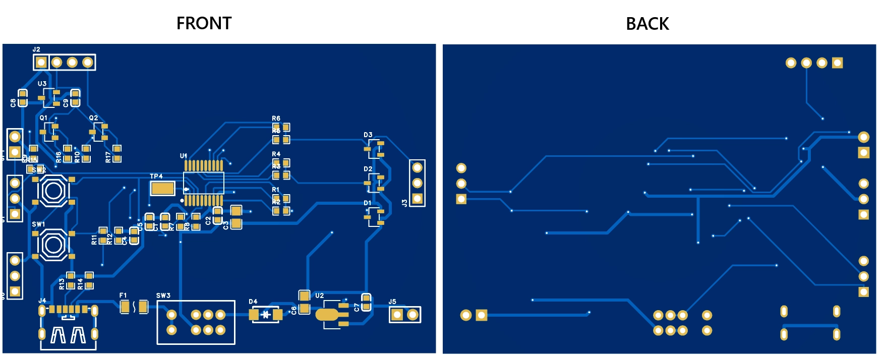
Figure: Fully routed 2D view of final PCB
The routing pipeline:
1. Export pad positions and nets from the open PCB to pads.json through the bridge.
2. Build the DSN with gen_dsn.py: 10 mil signal traces, 20 mil power traces, 8 mil clearance, and vias with a 12 mil drill and a 24 mil pad.
3. Run Freerouting v2.1.0 headless on Java 21. Releases from v2.2.0 onward require Java 25.
|
|---|
4. Check the returned SES file with check_ses.py, which must report "open nets 0".
5. Import the routes with import_ses.mjs, placing vias first and tracks second.
6. Run PCB DRC, then rebuild the copper pours.
What Claude Code Cannot Do in PCB Design Yet
In this workflow, Claude Code did not directly see the PCB layout. Instead, it worked with component coordinates and data returned by the EasyEDA Pro API. While it could create and modify the design, several important checks still required manual review:
- Visual inspection: Checking component placement, trace routing, spacing, and the overall PCB layout.
- 3D clearance: Verifying component heights, connector positions, and mechanical fit using the PCB's 3D view.
- Thermal checks: Reviewing components that may generate heat and ensuring sufficient copper area for heat dissipation.
- Datasheet verification: Checking pinouts, footprints, component dimensions, and electrical specifications against manufacturer datasheets.
- Component selection: Reviewing part substitutions, checking JLCPCB stock availability, and confirming that replacements meet the design requirements.
These checks are important because passing a Design Rule Check (DRC) does not guarantee that a PCB is electrically correct, mechanically suitable, or ready for manufacturing.
For a broader comparison of tools used at different stages of PCB development, see AI Tools for PCB Design.
The open items when the scripts finished:
- Visual review: No one had visually reviewed the routed layout. Silkscreen overlaps, part orientation, and overall placement still need a human pass.
- SW3 slide switch: Its footprint pins are unevenly spaced, and the schematic assumes the slider shorts adjacent pins. The real contact layout and actuator direction need the datasheet drawing.
- USB-C edge: Whether the receptacle must overhang the board edge is a mechanical check.
- Battery polarity: J5 assumes pin 1 is +9 V, because the source PDF was ambiguous.
- MCU sourcing: The CH32V006 must be consigned, or the design switches to the V005.
- Manufacturing files: The Gerber, BOM, and pick-and-place (CPL) files still need to be exported and inspected.
- In-built human steps: Project creation, the Apply click, the DRC log, and every approval.
- Bridge stability: Low memory caused the bridge process to terminate twice while it was running as a Claude Code background task. Running it as a standalone process fixed this.
Conclusion
Claude Code PCB design works on real projects. Using EasyEDA Pro, I converted a 47-component, three-page schematic from a PDF into a fully routed PCB with zero DRC errors, demonstrating how AI can assist in the PCB design process.
Use it for placement, wiring, and routing, and verify each step with scripts that read back the design. Keep visual review, mechanical checks, and sourcing decisions with an engineer, and you get a verified layout without giving up control of the board.
- Once your design passes review, take it to manufacturing with JLCPCB. Upload your PCB files and get an instant quote to move from a verified design to a physical board.
FAQs About Claude Code PCB Design
Q: Can Claude Code Design a PCB on Its Own?
No. Claude Code can place, wire, and route a real board through the EasyEDA API, but it does not see the canvas. Visual review, mechanical checks, and sourcing still need an engineer.
Q: Does EasyEDA Pro Have an API for AI Agents?
Yes. The EasyEDA API skill exposes the EasyEDA Pro JavaScript API via a local bridge, allowing Claude Code and similar agents to run code in the open editor.
Q: Does the EasyEDA Pro API Include an Autorouter?
Not in version 3.2.149. Its API has no autorouting call, so this build routed the board in Freerouting and imported the routes through the bridge.
Q: How Do I Secure the EasyEDA API Bridge?
Run it only while you work, and stop it afterward. In skill version 1.1.43, the bridge has no authentication, so add a shared token and an Origin check to bridge-server.mjs.
Q: Why Does EasyEDA Say Component Attributes Do Not Match the Supplier Part?
Parts placed through the EasyEDA Pro 3.2.149 API lose their supplier attributes. Rewriting the supplier ID, MPN, manufacturer name, and other properties in a single modify() call clears the warning.
Popular Articles
• AI Tools for PCB Design: Which Tool Fits Your Workflow Stage?
• AI PCB Design: From Prompt to PCB with EasyEDA Pro
• GPT-6 Astra PCB Design in KiCad: From Brief to Verified Native Project
• GPT-6 Astra PCB Design in EasyEDA Pro: What Worked, What Failed, and What We Learned
• How to Design Your Own Keyboard PCB: From Layout to Firmware
Keep Learning
Claude Code PCB Design: Can It Build a Real Board in EasyEDA Pro?
Key Takeaways Claude Code PCB design: Using Claude Opus 5.5 and EasyEDA Pro 3.2.149, I converted a 47-component, three-page schematic from a PDF into a fully routed, two-layer PCB with zero DRC errors. EasyEDA Pro integration: The EasyEDA API skill connects Claude Code to EasyEDA Pro through a local bridge server and the Run API Gateway extension. This allows Claude to control the editor via JavaScript, with a 30-second timeout per API call. Design verification: A successful API response doesn't alway......
How to Design a PCB with Flux.ai (Step-by-Step Guide)
Key Takeaways This step-by-step Flux PCB design tutorial demonstrates the complete workflow by creating a compact 15 × 15 mm USB 2.0 hub, refining the layout, routing high-speed differential traces, and preparing manufacturing files for JLCPCB PCB fabrication and assembly. We are all hearing news; new AI models are being released every month. And it has finally reached the schematic editor. Flux.ai is a browser-based AI PCB design tool with a built-in AI agent that behaves like a junior hardware engin......
AI Tools for PCB Design: Which Tool Fits Your Workflow Stage?
AI tools can now assist with PCB architecture, schematic generation, component selection, placement, routing, and design verification. However, different tools target different stages of the PCB workflow. This guide compares AI tools for PCB design based on what they actually do, what inputs they require, and where they fit within a real engineering workflow. In this guide, you will learn: The 6 types of AI PCB tools and the input each one needs What AI PCB design tools do, compared stage by stage How......
AI PCB Design: From Prompt to PCB with EasyEDA Pro
Key Takeaways AI PCB design uses AI agents to automate schematic creation, component selection, layout, and verification inside a real EDA editor — not just generate images. The workflow connects EasyEDA Pro to an AI coding agent (Claude Code or Codex) through the EasyEDA API Gateway, the open-source API Skill, and a local bridge server. Setup takes about ten minutes and is fully local-first: designs, API calls, and intermediate code never leave your machine. Because the agent places real library part......
GPT-6 Astra PCB Design in KiCad: From Brief to Verified Native Project
Key Takeaways What OpenAI published: The launch page features a 15-second condensed clip of GPT-6 Astra performing PCB layout in KiCad. What the model did: It turned a four-line brief into a 44 × 34 mm, two-layer PCB, covering the circuit, footprints, component placement, routing, and a native two-sheet schematic. Where the work went: Placement and routing were only part of the work. Two linked schematic sheets, project-local libraries, and UUID-based links between 45 components and their footprints w......
GPT-6 Astra PCB Design in EasyEDA Pro: What Worked, What Failed, and What We Learned
Key Takeaways What was tested: GPT-6 Astra was given access to a native EasyEDA Pro 3.2.149 installation and asked to design a stereo TPA3116D2 amplifier from a four-line written brief. What it produced: The run resulted in a 44 × 34 mm, two-layer PCB with 40 SMD components and an editable native EasyEDA Pro project with embedded libraries. Where it failed: The first complete import opened cleanly and looked plausible, yet the initial native verification reported 50 association mismatches involving 12......