How to Design a PCB with Flux.ai (Step-by-Step Guide)
12 min
- What Is Flux.ai?
- The Project Brief: A USB Hub That Fits Inside a Laptop
- Step 1: Create a Project and Choose a Custom Build
- Step 2: Write a Clear Prompt for the AI Agent
- Step 3: The AI Plans the Design and Writes Its Own Notes
- Step 4: AI Component Selection and Netlist Building
- Step 5: Review the AI-Generated Schematic
- Step 6: Automated Design Checks
- Step 7: The AI Generates the Board Outline and Placement
- Step 8: Refine the Placement and Route It Yourself
- Step 9: Export the Gerber, BOM, and CPL Files from Flux.ai
- Step 10: Order the PCB from JLCPCB
- Conclusion
- FAQs about Flux.ai

Key Takeaways
This step-by-step Flux PCB design tutorial demonstrates the complete workflow by creating a compact 15 × 15 mm USB 2.0 hub, refining the layout, routing high-speed differential traces, and preparing manufacturing files for JLCPCB PCB fabrication and assembly.
We are all hearing news; new AI models are being released every month. And it has finally reached the schematic editor.
Flux.ai is a browser-based AI PCB design tool with a built-in AI agent that behaves like a junior hardware engineer. You just have to describe the product, and it plans the architecture, selects components, wires the schematic, runs electrical checks, and even places the board for you. The obvious question is whether the output is actually manufacturable, or just a pretty demo.
To find out, we are designing a USB 2.0 hub with two downstream ports on a PCB with a form factor of 15 × 15 mm. Small enough to tuck inside a laptop.
In this Flux.ai PCB design tutorial, we will walk through the complete workflow, from the first AI prompt to the finished layout. I will show how to export the Gerber, BOM, and CPL files and order the board from JLCPCB.
What Is Flux.ai?
Flux.ai is a cloud EDA platform that runs entirely in the browser. When you create a new project, Flux.ai asks, "What do you want to build?" And offers guided templates from a beginner blinking LED to an advanced motor controller for a robot arm.
The fourth card: "Your own idea - Start from scratch." Since there is a lot of diversity in hardware design, I have chosen a custom design of a laptop-internal USB hub, which is not exactly a template project.
I started on the free plan, which includes some AI credits. That is enough to run a small project like this one end-to-end. Manual schematic and PCB editing is unlimited on the free tier, so the credits are only consumed when the AI agent does work for you.
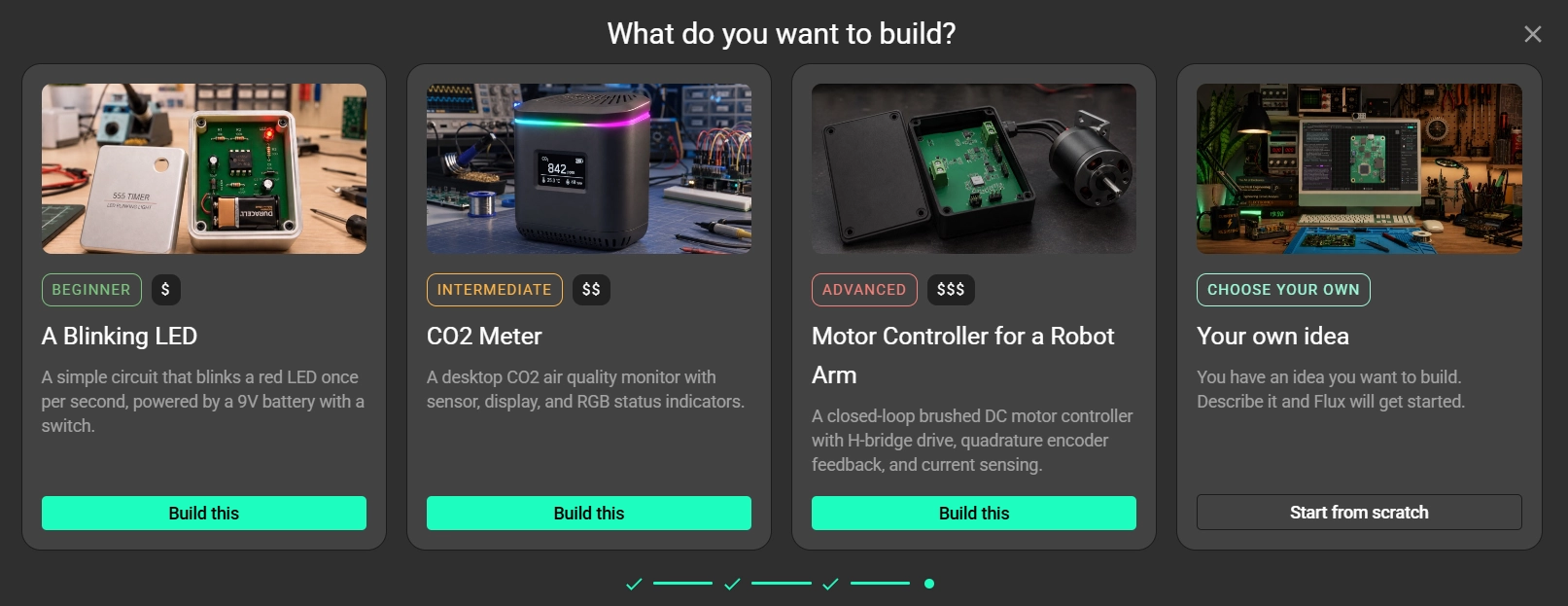
Fig1. The Flux build template
The Project Brief: A USB Hub That Fits Inside a Laptop
| Requirement | Target |
|---|---|
| Function | USB 2.0 high-speed hub with 1 upstream and 2 downstream ports |
| Board size | 15 × 15 mm maximum |
| Upstream connection | 4 soldered wires only to USB |
| Downstream connection | Soldered wires to pads |
| Stack-up | 4-layer with controlled impedance |
Step 1: Create a Project and Choose a Custom Build
The workspace has three zones: the AI chat panel on the left, the working area in the middle (Files, Schematic, and PCB tabs), and the components and library panel on the right, where you can search parts or manage project properties.
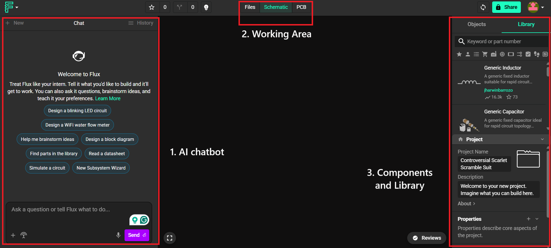
Fig2. Flux workplace
Step 2: Write a Clear Prompt for the AI Agent
Everything depends on the quality of the prompt, so I kept it specific to the function and the hard size limit:
"I want to make a small USB hub which fits inside my laptop, PCB should be under 15x15mm, and I need USB2.0 with 2 downstream ports."
The response is where Flux.ai first impressed me. Instead of blindly drawing something, the agent evaluated feasibility and proposed an architecture.
Answer was like: a compact hub controller IC with one upstream and two downstream ports, solder pads instead of connectors to stay inside the size budget, bus-powered operation from the laptop's 5 V rail, ESD protection arrays on every D+/D− pair, and a 4-layer PCB for signal integrity at this density.
It then asked me to choose between five connection methods: solder pads, an FPC connector, a board-to-board connector, or repurposing an existing internal USB device. I confirmed: four soldered wires on the upstream side, and soldered wires on both downstream ports, too.
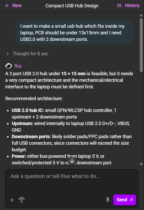
Fig3. Flux.ai AI agent: the junior hardware designer
Then, with a few more questions and answers, Flux.ai and I arrived at the same plot and agreed on the final design.
Step 3: The AI Plans the Design and Writes Its Own Notes
Once the interface question was settled, the agent generated a plan. It has created a "USB Hub Design Notes" document inside the project files. It records the requirements, the implemented architecture, layout status, verification status, and a candid list of open risks. You can refine or query the document directly from the editor.
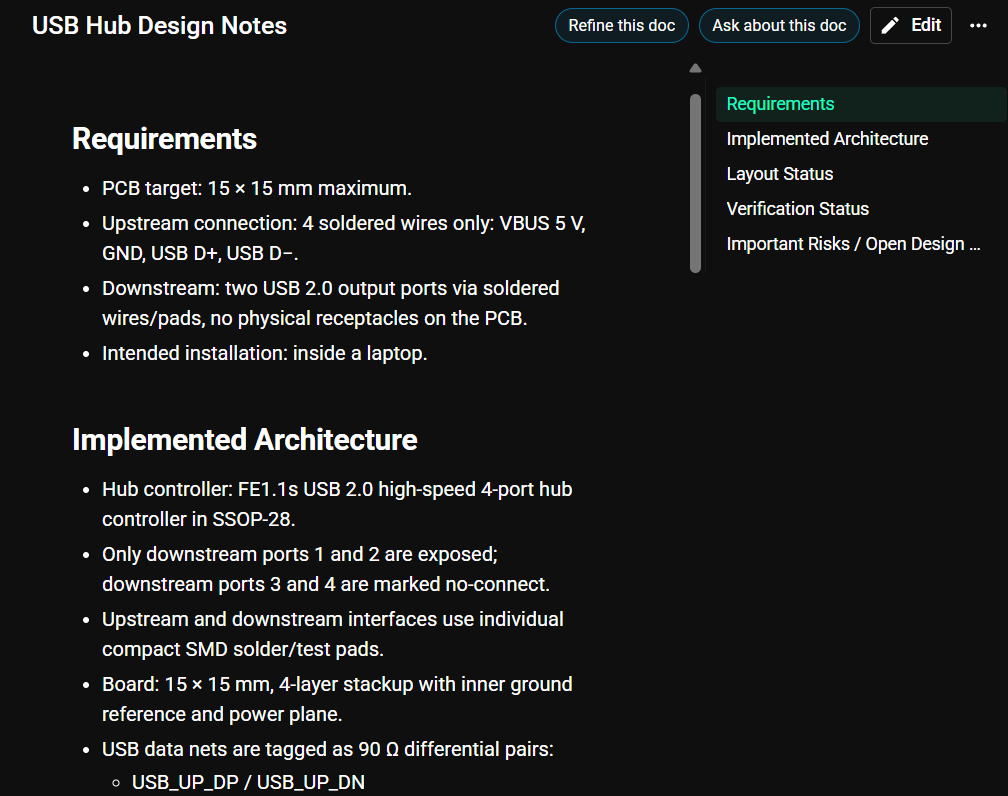
Fig4. Flux automatically created USB Hub Design Notes document
For anyone who has inherited an undocumented board, an EDA tool that documents its own decisions as it works is a quietly big deal.
Step 4: AI Component Selection and Netlist Building
So after the plan, the game of component selection begins, selecting the FE1.1s USB 2.0 high-speed hub controller from Terminus Technology in an SSOP-28 package. It chose this part because Flux's library had a usable, which is an availability-driven decision rather than a purely theoretical one.
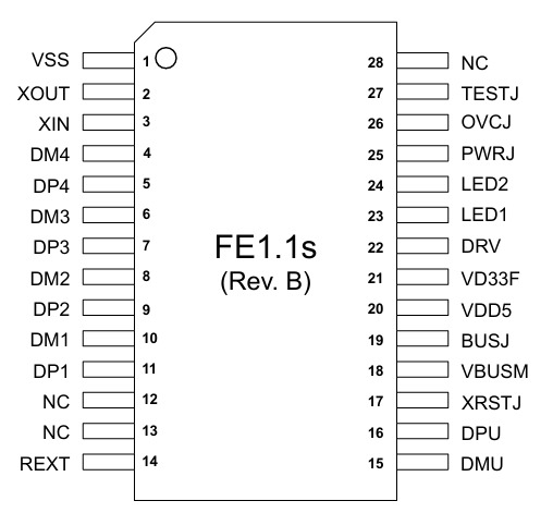
Fig5. FE1.1s Pin diagram
The FE1.1s is technically a 4-port hub, so the design exposes downstream ports 1 and 2 and marks ports 3 and 4 as no-connect.
The IC pulls its weight in a constrained design like this: it integrates the USB 2.0 transceivers, the upstream 1.5 kΩ pull-up and downstream 15 kΩ pull-downs, 5 V-to-3.3 V and 1.8 V regulators, a power-on-reset circuit, and a 12 MHz oscillator with an internal PLL that multiplies up to the 480 MHz high-speed clock. Every one of those integrated blocks is an external component we do not have to fit on a 15 × 15 mm board.
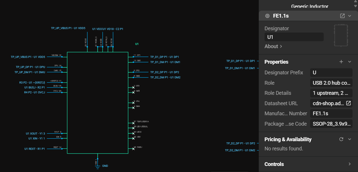
Fig6. Placement of parts in Flux
As it placed the parts, the agent built the netlist itself by naming the USB data nets (USB_UP_DP/DN for upstream, USB_D1 and USB_D2 pairs for the two downstream ports) and tagging all three pairs as 90 Ω differential. This is the correct USB 2.0 differential impedance, and will drive the routing rules later.
Step 5: Review the AI-Generated Schematic
Within a few minutes, the agent had a complete, wired schematic. Here is the input (upstream) section: four solder pads for VBUS, GND, D+, and D−, with a USBLC6-2P6 ESD protection array sitting on the data lines before they reach the hub, and the decoupling network around the controller.
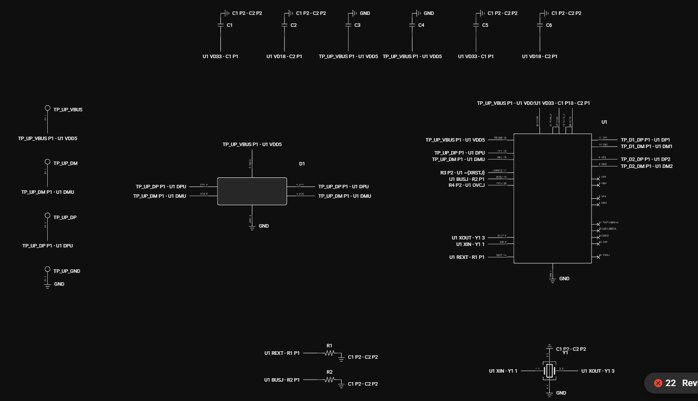
Fig7. Input side schematic of USB hub in Flux
The output section mirrors the same discipline on both downstream ports; each gets its own USBLC6-2P6 array and its own VBUS, D+, D−, and GND pads:
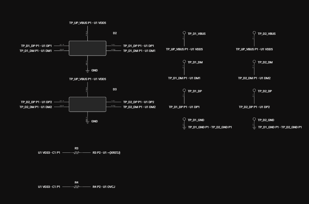
Fig8. Output side schematic of USB hub in Flux
And the full schematic ties it together as:
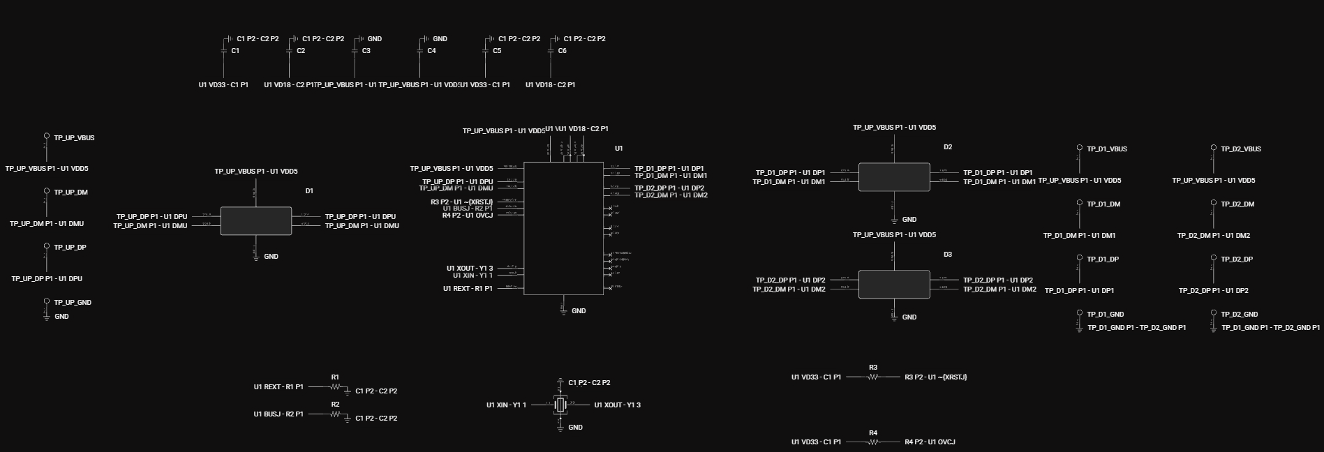
Fig9. Full schematic of USB hub in Flux
The support circuitry follows the FE1.1s datasheet's application requirements closely, which is exactly what I would check first in any AI-generated design:
- Power: upstream VBUS feeds the VDD5 pin; the internal regulator outputs VD33_O and VD18_O, which are tied to their supply pins with proper decoupling.
- Clock: a 12 MHz SMD crystal on XIN/XOUT.
- Configuration: BUSJ is pulled low for bus-powered operation, XRSTJ is pulled high to the 3.3 V rail, and OVCJ is tied high because this minimal version has no overcurrent-monitoring switch. REXT gets its precision bias resistor, and unused LED/EEPROM pins are left unconnected.
Step 6: Automated Design Checks
Flux.ai runs a continuous review suite, and the agent re-checks its own work after building the schematic.
The electrical rule checks, like driver conflicts, duplicate designators, floating pins, no-connect violations, pin-to-pin conflicts, shorted components, missing power, and single-pin nets, are all passed.
The only open items at this stage were design-rule errors, and every one of them was an airwire: the ratsnest of a board that is placed but not yet routed. That is not a defect; it is a to-do list.
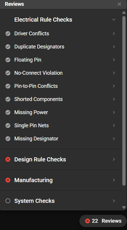
Fig10. Automatic design rule checking in Flux
Step 7: The AI Generates the Board Outline and Placement
Switching to the PCB tab, the agent had already generated a 15 × 15 mm board outline on a 4-layer stack-up with a stackup like: signal on top and bottom, with an inner ground reference plane and a power plane between them.
Then AI runs an auto component placement according to the design. The placement logic was sensible; the main controller sits in the center, upstream solder pads on the left, downstream port 1, and port 2 pads sit on the upper and right edge, respectively. Each ESD array landed next to the pad group it protects, and small passives were placed onto the bottom layer.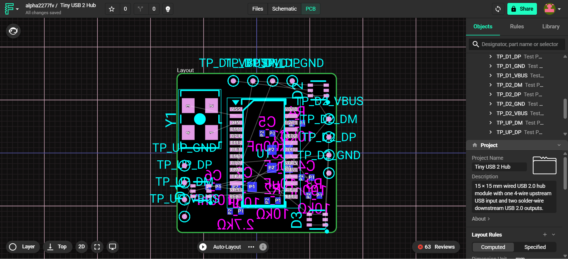
Fig11. Board outline and placement in Flux
Step 8: Refine the Placement and Route It Yourself
This is where I took over. The auto-placement was a solid 80% starting point, but on a board this dense. The last 20% is the difference between routable and non-routable. 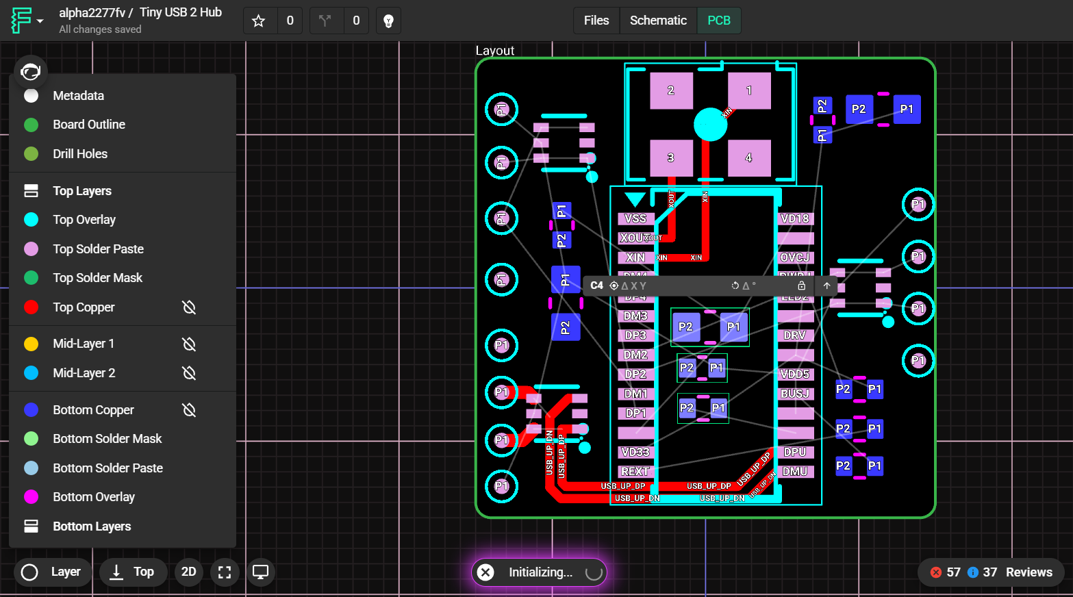
Fig12. Refining the PCB routing in Flux
I choose to route manually rather than rely on the autorouter. The rules I held myself to are the standard ones for any high-speed differential interface: keep each 90 Ω pair short, tightly coupled, and length-matched. Power distribution and ground stitching filled in around the signal work.
After routing, the airwire errors cleared, and the board passed its checks. Total time from first prompt to finished layout: a single sitting, the AI handled the hours of schematic capture and library work, and I spent my time where human judgment actually adds value.
Step 9: Export the Gerber, BOM, and CPL Files from Flux.ai
Flux.ai exports standard fabrication outputs, so moving from the cloud editor to a manufacturer is painless.
From the project menu in the top-left corner, choose Export > Manufacturing Files (Gerbers, etc.) (.zip). The same Export menu also provides Bill of Materials (.zip) and Pick & Place (.zip) — the three deliverables an assembly service needs.
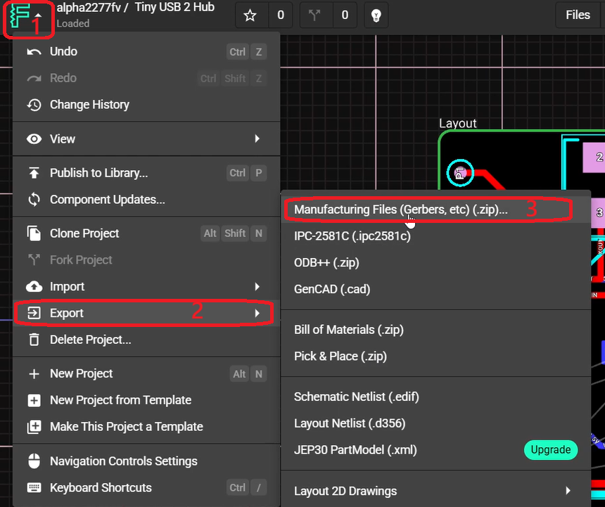
Fig13. Fabrication files generation in Flux
The manufacturing archive unpacks into a complete, conventionally named file set — copper layers for all four layers (f_cu, in1_cu, in2_cu, b_cu), solder mask, paste, and silkscreen Gerbers for both sides, the board outline (edge_cuts), an NC drill file, a D356 netlist for electrical test, the BOM folder, and a pick_and_place.csv:
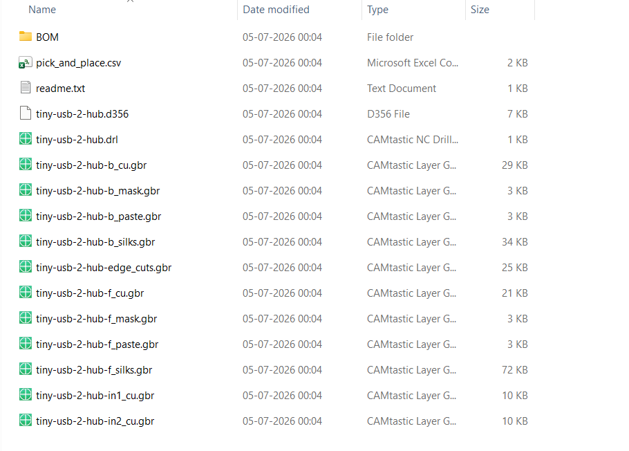
Fig14. Gerber file exported from Flux
| File | What it is | Who uses it |
|---|---|---|
| _cu.gbr, _mask.gbr, _paste.gbr, _silks.gbr | Copper, solder mask, paste, and silkscreen Gerber layers | PCB fabrication |
| edge_cuts.gbr | Board outline | PCB fabrication |
| .drl | NC drill file | PCB fabrication |
| .d356 | IPC-D-356 netlist | Electrical testing |
| BOM folder | Bill of materials with part numbers | Assembly (component sourcing) |
| pick_and_place.csv | Component positions and rotations | Assembly (SMT placement) |
Step 10: Order the PCB from JLCPCB
With the files in hand, the JLCPCB ordering flow takes only a few minutes:
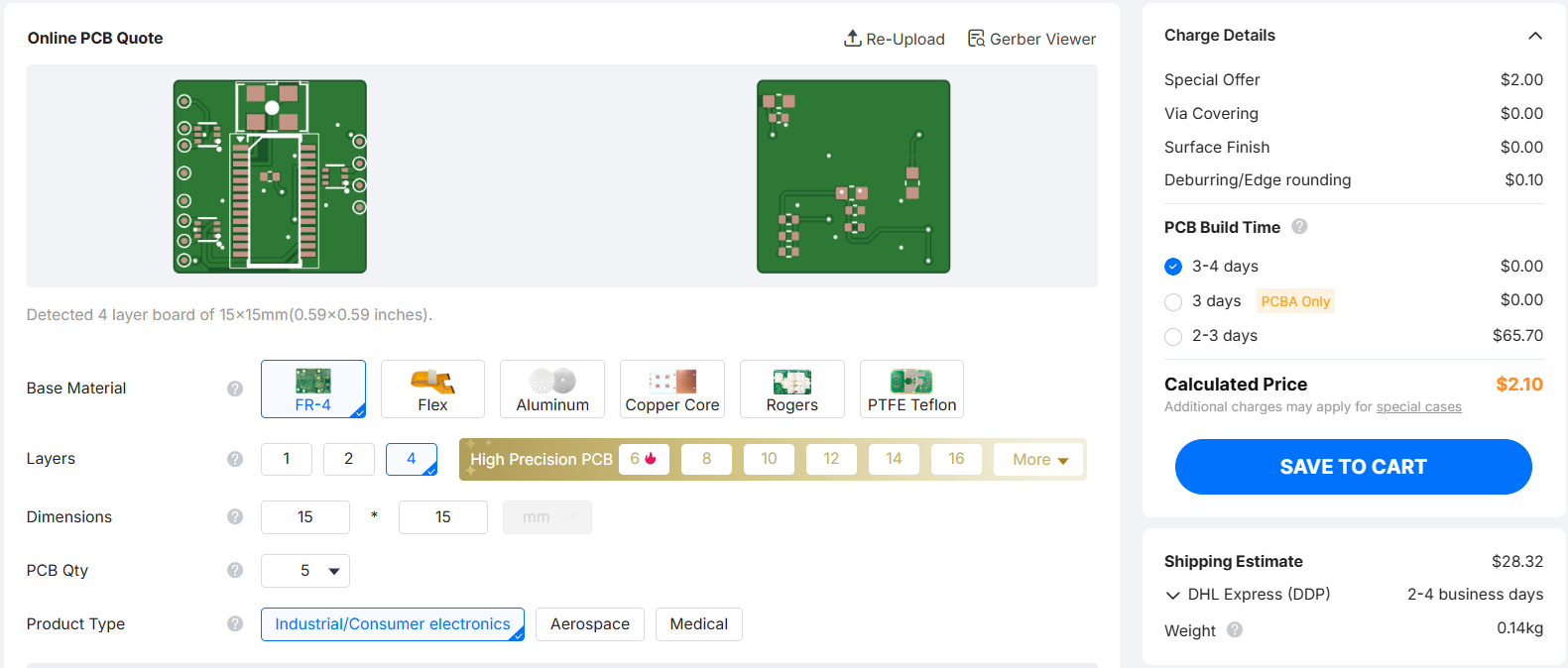
Fig15. Order the PCBs from JLCPCB
- Upload the Gerbers: On the JLCPCB quote page, upload the manufacturing .zip straight from Flux. The viewer reads the board outline and layer count automatically and renders a preview.
- Set the fabrication options: Confirm the 4-layer stack-up and the 15 × 15 mm dimensions, then pick quantity, thickness, and surface finish.
If you want a fully assembled PCB, toggle on SMT assembly, and choose the side to assemble.
Then load the BOM and the pick_and_place.csv (CPL) exported from Flux. After matching the components and going through the list, place an order.
A few days later, a fully assembled 15 × 15 mm hub arrives, from a one-sentence prompt to a manufactured board with almost all of the schematic capture done by an AI agent.
Conclusion
Flux.ai did not replace the engineer in this project; it just changed the workflow. I spent almost half of the time building custom components, symbols, and footprints. The schematic work has also been reduced because it directly takes the data from the schematics; the work that used to take 10 hours now takes almost 2 hours. The AI agent turned a one-sentence brief into a correctly-architected, ERC-clean schematic with sensible component choices. The human work concentrated exactly where it should: refining placement, and judging the power-architecture trade-offs the AI flagged.
Just as importantly, the output is completely standard. The Gerber, BOM, and CPL files that Flux.ai exports drop into JLCPCB's fabrication and assembly flow without any conversion, and every component in this design comes from the stocked parts library.
FAQs about Flux.ai
Q: Is Flux.ai free to use?
Yes. The free plan includes unlimited manual schematic and PCB editing, plus a starter allowance of AI credits, which was enough to complete this hub design. Paid plans add a larger monthly allowance of AI compute units for heavier agent use.
Q: Can the Flux.ai agent design a complete PCB without human input?
It extends impressively to architecture, component selection, a checked schematic, board outline, and placement. But it left the board unrouted, and high-speed routing, placement refinement, and power-architecture decisions.
Q: Does JLCPCB accept fabrication files exported from Flux.ai?
Yes. Flux.ai exports industry-standard Gerbers, an NC drill file, a BOM, and a pick-and-place CSV. They upload to JLCPCB's quote and assembly system exactly like files from KiCad or Altium, with no conversion needed.
Popular Articles
• AI Tools for PCB Design: Which Tool Fits Your Workflow Stage?
• AI PCB Design: From Prompt to PCB with EasyEDA Pro
• GPT-6 Astra PCB Design in KiCad: From Brief to Verified Native Project
• GPT-6 Astra PCB Design in EasyEDA Pro: What Worked, What Failed, and What We Learned
• How to Design Your Own Keyboard PCB: From Layout to Firmware
Keep Learning
Mastering PCB Design Rules: A Comprehensive Guide for Optimal Results
Key Takeaways Follow core PCB design rules for reliable electrical and mechanical performance. Optimize trace width, spacing, impedance, and vias for signal integrity and manufacturability. Apply DFM and DRC early to identify potential manufacturing and layout issues. Consider thermal management, grounding, and testing during the PCB design stage. Align design rules with your PCB manufacturer’s capabilities to improve production reliability and reduce redesigns. PCB design rules are essential guidelin......
KiCad MCP: How to Design a PCB with Claude Code [Step-by-Step]
Key Takeaways Claude can design PCBs in KiCad: By connecting Claude to KiCad through an MCP server, you can use AI to create and modify PCB designs. In this project, Claude helped turn a 5 A XL4015 buck converter netlist into a two-layer, 63 × 33 mm PCB layout with zero ERC violations and zero DRC errors after minor initial fixes. Set up Claude securely: Use a KiCad MCP server that starts in read-only mode. Review the server code before installing it, connect through stdio, and allow editing only in a......
Claude Code PCB Design: Can It Build a Real Board in EasyEDA Pro?
Key Takeaways Claude Code PCB design: Using Claude Opus 5.5 and EasyEDA Pro 3.2.149, I converted a 47-component, three-page schematic from a PDF into a fully routed, two-layer PCB with zero DRC errors. EasyEDA Pro integration: The EasyEDA API skill connects Claude Code to EasyEDA Pro through a local bridge server and the Run API Gateway extension. This allows Claude to control the editor via JavaScript, with a 30-second timeout per API call. Design verification: A successful API response doesn't alway......
How to Design a PCB with Flux.ai (Step-by-Step Guide)
Key Takeaways This step-by-step Flux PCB design tutorial demonstrates the complete workflow by creating a compact 15 × 15 mm USB 2.0 hub, refining the layout, routing high-speed differential traces, and preparing manufacturing files for JLCPCB PCB fabrication and assembly. We are all hearing news; new AI models are being released every month. And it has finally reached the schematic editor. Flux.ai is a browser-based AI PCB design tool with a built-in AI agent that behaves like a junior hardware engin......
AI Tools for PCB Design: Which Tool Fits Your Workflow Stage?
AI tools can now assist with PCB architecture, schematic generation, component selection, placement, routing, and design verification. However, different tools target different stages of the PCB workflow. This guide compares AI tools for PCB design based on what they actually do, what inputs they require, and where they fit within a real engineering workflow. In this guide, you will learn: The 6 types of AI PCB tools and the input each one needs What AI PCB design tools do, compared stage by stage How......
AI PCB Design: From Prompt to PCB with EasyEDA Pro
Key Takeaways AI PCB design uses AI agents to automate schematic creation, component selection, layout, and verification inside a real EDA editor — not just generate images. The workflow connects EasyEDA Pro to an AI coding agent (Claude Code or Codex) through the EasyEDA API Gateway, the open-source API Skill, and a local bridge server. Setup takes about ten minutes and is fully local-first: designs, API calls, and intermediate code never leave your machine. Because the agent places real library part......