Designing a Precision 72-LED Wearable Watch: Building a 40mm Round PCB with JLCPCB SMT Assembly
10 min
- Introduction and Motivation
- System Architecture and Component Selection
- PCB Layout and Wearable DFM Engineering
- One-Stop PCBA Assembly via JLCPCB and LCSC
- Assembly, Firmware and Enclosure Integration
- Firmware Optimization and LED Multiplexing
- Project Feedback and Experience
- FAQ about the 72-LED Wearable Watch
Key Takeaways
This case study explores the design and fabrication of a 72-LED wearable watch built on a precision 40mm round PCB. Learn how JLCPCB SMT assembly eliminated hand-soldering 70+ 0603 LEDs, how ENIG surface finish ensures reliability in wearable applications, and how a clever panelization strategy with mouse-bite breakaway tabs enabled automated assembly of a circular board. The project demonstrates a complete workflow from EasyEDA schematic capture to firmware optimization and commercial-grade stainless steel enclosure integration.
Introduction and Motivation
Building custom wearable hardware remains one of the most rewarding yet challenging domains in modern electronics. While off-the-shelf smartwatches rely on complex OLED screens and power-hungry processors, open-source project creator Taifur set out to create a minimalist, industrial-grade timepiece: The LED Round Watch.
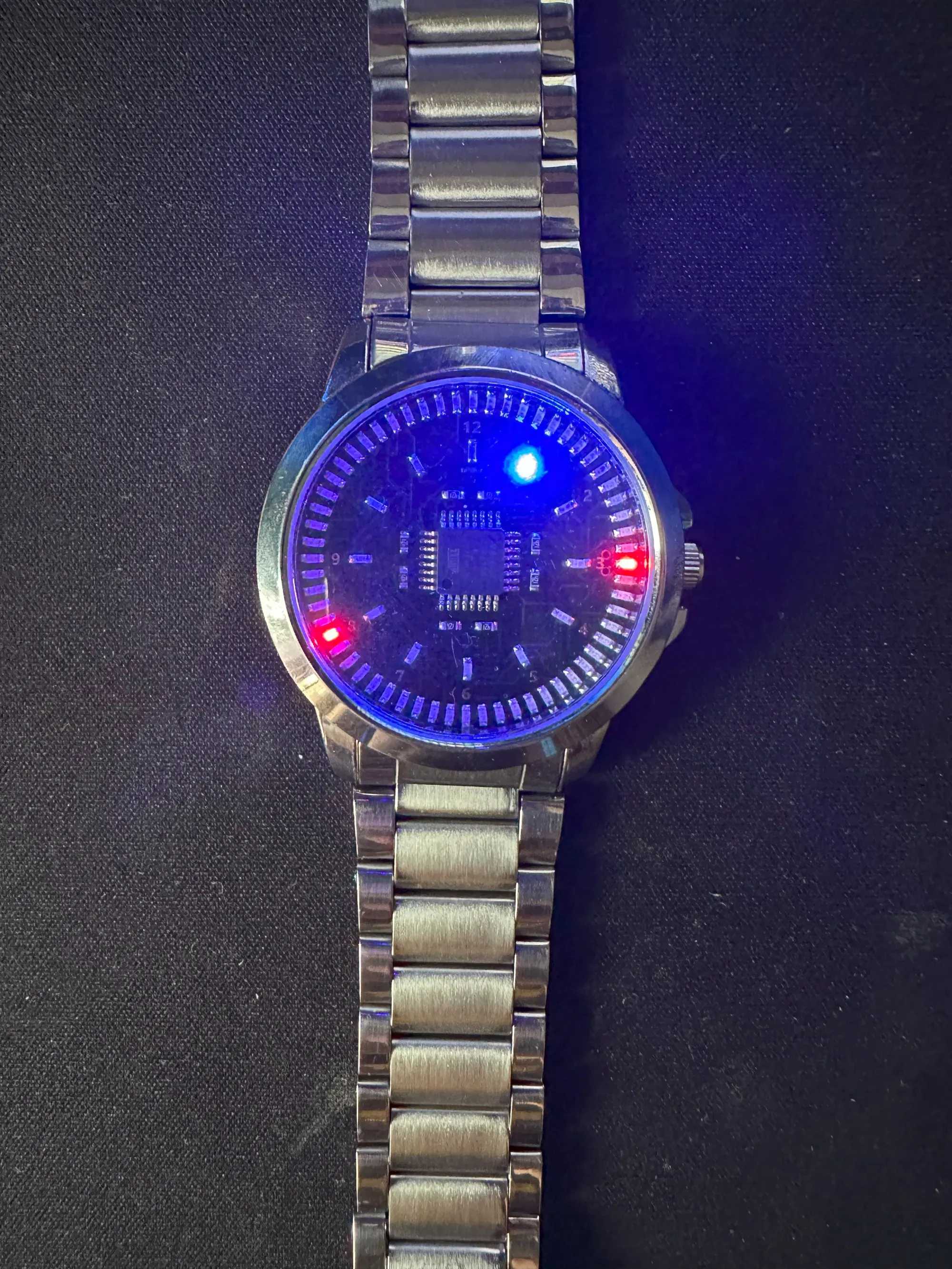
The core vision was simple yet technically demanding: build a wristwatch driven by a ring of 72 individual SMD LEDs powered by an ATmega328P microcontroller and a high-precision DS3231 Real-Time Clock (RTC).
However, translating a 72-LED radial circuit into a wearable form factor presents major engineering hurdles:
- Mechanical Constraints: The total PCB diameter could not exceed 40mm to fit inside a commercial off-the-shelf watch case.
- Assembly Complexity: Hand-soldering over 70 surface-mount LEDs alongside fine-pitch ICs (TQFP-32 package) on a 40mm board is prone to bridging, misalignment, and thermal stress.
- Aesthetic Minimalism: No unsightly headers, bulky connectors, or loose wiring could be visible on the display face.
To overcome these obstacles, Taifur turned to EasyEDA for schematic capture and PCB layout, and relied on JLCPCB PCB Assembly (PCBA) service to manufacture and assemble the high-density board in one seamless workflow.
System Architecture and Component Selection
To ensure long-term timekeeping accuracy and sleek visual dynamics, the hardware architecture was structured into four core functional blocks:
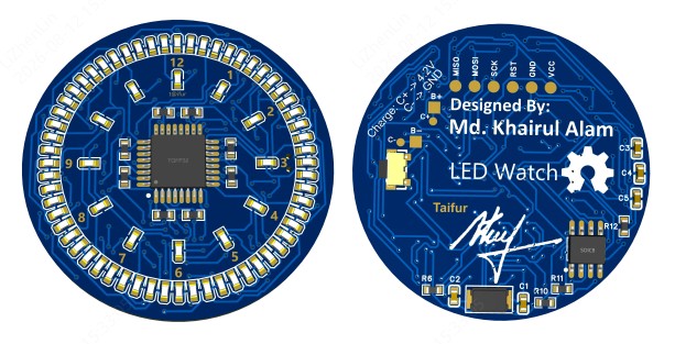
Hardware Specifications Overview
| Subsystem | Component | Package / Specs | Function |
|---|---|---|---|
| Main Processing Unit | Microchip ATmega328P-AU | TQFP-32 (0.8mm pitch) | Drives LED multiplexing matrix & I2C time reading |
| Real-Time Clock (RTC) | Maxim Integrated DS3231MZ | SOIC-8 / TCXO | Maintains ±2ppm timekeeping accuracy |
| Hour Display | 12x SMD LEDs | 0603 Package (Blue) | Indicates hours (1 through 12 position) |
| Minute / Second Display | 60x SMD LEDs | 0603 Package | Indicates minutes and seconds in a 360° ring |
| Current Limiting | 8x SMD Resistor Networks | 0603 / 0805 | Prevents LED thermal runaway and regulates brightness |
| Power Source | CR2032 / LIR2032 Coin Cell | 3V SMD Battery Holder | Compact power supply mounted on bottom PCB |
| Programming Interface | 6x Exposed Pogo Pin Pads | 2.54mm Pitch Gold Pads | ISP / UART firmware flashing interface |
Key Circuit Design Details
- Main Processor ATmega328P-AU: Chosen for its wide community support and low standby current in sleep modes, the ATmega328P in a TQFP-32 package provides sufficient I/O pins to drive the multiplexed LED array while maintaining an ultra-thin physical profile.
- High-Precision Timekeeping DS3231 RTC: Unlike standard RTCs that rely on external 32.768 kHz crystals, the DS3231 features an integrated Temperature-Compensated Crystal Oscillator (TCXO). This guarantees an accuracy of ±2 minutes per year, essential for a standalone wristwatch without Wi-Fi or Bluetooth sync.
- Radial 72-LED Matrix: The watch face uses 12 Blue 0603 LEDs for hours and 60 SMD LEDs for minutes/seconds. By using multiplexed matrix driving controlled by 8 current-limiting resistors, the ATmega328P can individually illuminate any hour/minute/second LED combination without requiring bulky LED driver ICs.
PCB Layout and Wearable DFM Engineering
Designing a circular PCB for a wearable product requires strict adherence to Design for Manufacturing (DFM) guidelines to ensure structural integrity and flawless SMT component placement.
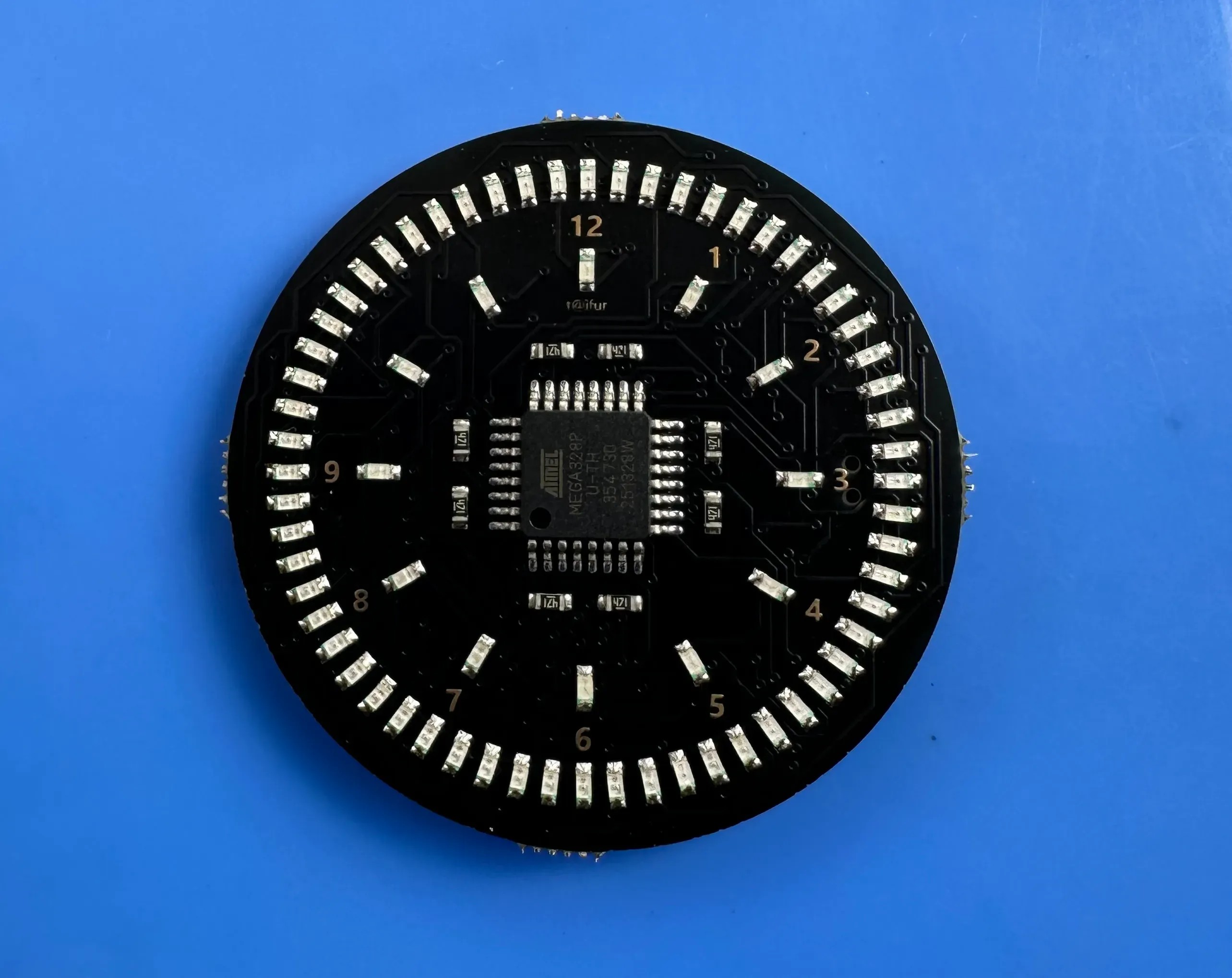
Double-Sided Component Layering Strategy
To maintain a high-end commercial aesthetic, component placement was split logically across both sides of the board:
- Top Layer (Display Face): Houses only the ATmega328P MCU, the 72 radially aligned LEDs, and 8 current-limiting SMD resistors. This creates a symmetrical, minimalist face reminiscent of precision analog watch dials.
- Bottom Layer (Utility & Power): Houses the DS3231 RTC, decoupling capacitors, time-adjustment tactile push button, coin-cell battery clip, and programming pads.
JLCPCB Manufacturing Parameters and DFM Compliance
| Parameter | Specification / Value |
|---|---|
| Board Layers | 2-Layer FR-4 |
| Board Diameter | Exactly 40.0 mm |
| PCB Thickness | 1.0 mm (Optimized for Watch Case) |
| Outer Copper Weight | 1 oz (35 µm) |
| Surface Finish | ENIG (Electroless Nickel Immersion Gold) |
| Solder Mask Color | Matte Black / Dark Green |
| Silkscreen Color | High-Contrast White |
| Min Trace Width / Clearance | 5 mil / 5 mil (0.127mm) |
| Min Via Hole Size | 0.3 mm drill / 0.5 mm pad |
| Edge-to-Copper Clearance | ≥ 0.3 mm (Prevents Shorts on CNC Routing) |
Why ENIG Surface Finish is Essential for Wearables
ENIG (Electroless Nickel Immersion Gold) was specified over standard HASL. ENIG offers two major advantages for wearable applications:
- Flat Surface Planarity: Crucial for solder joint reliability on fine-pitch components like the TQFP-32 ATmega328P and 0603 LEDs.
- Corrosion and Oxidation Resistance: Gold plating protects exposed pads—such as the 6 programming pads—from oxidation caused by ambient moisture or skin contact.
Panelization and Breakaway Frame (Mouse Bites)
Because a 40mm circular board cannot easily travel through automated SMT conveyor belts, the board was designed inside a rectangular carrier frame attached via mouse-bite breakaway tabs (stamp holes).
- Mouse Bite Hole Specs: 0.5mm diameter holes spaced at 0.8mm pitch along the 40mm circumference curve.
- CNC Milling: JLCPCB precision CNC routing cuts the 40mm circle accurately to within ±0.1mm, ensuring an exact drop-in fit into the stainless steel case.
One-Stop PCBA Assembly via JLCPCB and LCSC
One of the largest bottlenecks in projects involving 70+ SMD components is manual soldering. Hand-soldering 0603 LEDs in a tight 360-degree circle frequently results in misaligned components, solder bridges, or damaged LED lenses due to excessive soldering iron heat.
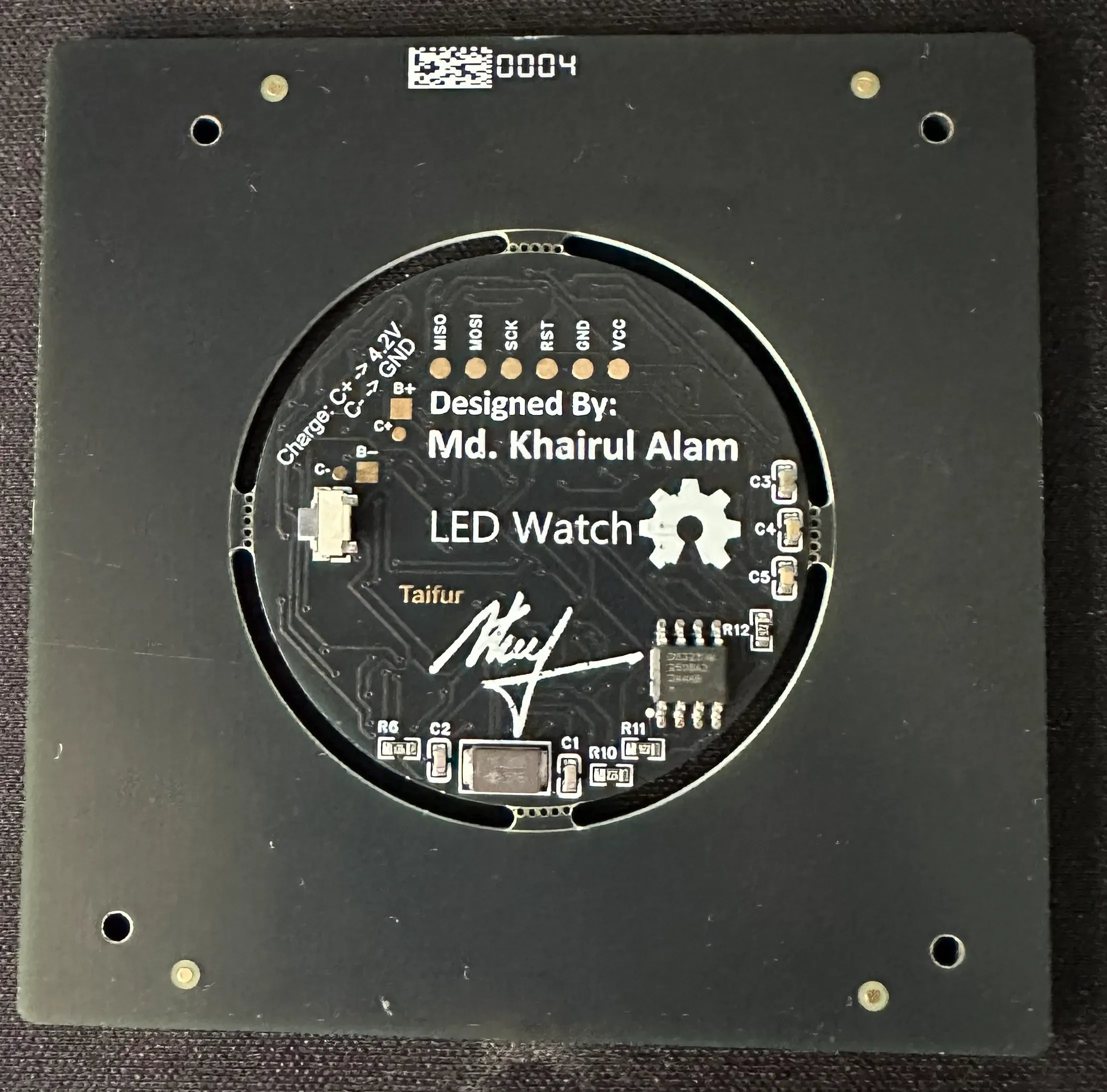
The JLCPCB Assembly Advantage
- LCSC Part Sourcing: All standard parts (ATmega328P, DS3231, 0603 LEDs, resistors, capacitors) were selected directly from the JLCPCB / LCSC Component Library, ensuring 100% stock availability and zero manual component sourcing delays.
- Automated CPL and BOM Matching: Uploading the BOM (Bill of Materials) and CPL (Component Placement List / Pick-and-Place file) generated from EasyEDA allowed JLCPCB online visualizer to instantly align all 72 LED footprints and rotation angles.
- Automated Optical Inspection (AOI): Every assembled board underwent AOI testing at the JLCPCB factory to guarantee zero tombstoned LEDs or pin bridging on the ATmega328P.
Assembly, Firmware and Enclosure Integration
Once the assembled PCBA arrived, finalizing the watch required four straightforward steps:
-
Separating the Board from the Carrier Frame
Using side flush cutters, the main circular watch PCB was snapped away from the outer rectangular carrier frame along the pre-scored mouse bites.
-
Firmware Upload via 6-Pin Pogo Pin Clip
Rather than soldering permanent header pins (which would prevent the PCB from lying flat inside the watch case), 6 exposed test pads were embedded on the bottom PCB layer connected to the ATmega328P ISP/UART lines (VCC, GND, RESET, MOSI, MISO, SCK). Using a 6-pin 2.54mm Pogo Pin Probe Clip connected to an Arduino UNO (configured as ISP) or USB-TTL adapter, firmware was uploaded in seconds without soldering a single wire.
-
Battery Installation and Power Wiring
A CR2032 / LIR2032 coin cell battery holder was secured to the bottom contacts. In deep-sleep mode, the ATmega328P consumes under 5 microamps, allowing the watch to run for months on a single coin cell while the DS3231 maintains accurate timekeeping.
-
Stainless Steel Enclosure Drop-In
Designing custom 3D-printed watch cases often results in bulky, fragile enclosures with poor water resistance. This project bypassed this issue by sourcing a commercial 40mm Stainless Steel Watch Case. Thanks to JLCPCB 1.0mm PCB thickness and precise 40mm CNC edge routing, the completed watch board dropped seamlessly into the steel casing, secured tightly by the threaded rear bezel.
Firmware Optimization and LED Multiplexing
The custom open-source Arduino sketch (led_round_watch.ino) controls timekeeping and display rendering efficiently.
Key Firmware Features
- Active Display Triggering: To preserve battery, the LEDs light up in a sleek sweeping animation upon pressing the bottom tactile button, displaying the time for 5 seconds before returning to low-power sleep.
- Time Adjustment Mode: Holding the tactile button enters setting mode, allowing the user to increment hours and minutes directly without connecting to a computer.
Project Feedback and Experience
Reflecting on the fabrication and assembly experience with JLCPCB, project designer Taifur shared:
"Designing a watch case from scratch with a 3D printer often looks unpolished and lacks durability. Using a commercial 40mm stainless steel case gave the watch a professional finish, but it meant the PCB had to be perfectly fabricated within exact dimensional limits.
Having JLCPCB assemble the top side with all 72 LEDs and the ATmega328P was a total game-changer. SMT soldering 70+ tiny LEDs by hand would have taken hours and had a high chance of failure. The ENIG finish looks incredible, the boards arrived in days, and everything worked flawlessly on the very first revision!"
FAQ about the 72-LED Wearable Watch
Q: How are all 72 LEDs controlled using an ATmega328P with limited GPIO pins?
The design employs multiplexed matrix driving with current-limiting resistors, enabling the ATmega328P to control the 12 hour LEDs and 60 minute/second LEDs individually without needing additional driver ICs.
Q: How do you program the watch without soldering bulky header pins?
Firmware is flashed via 6 exposed gold-plated pads on the bottom PCB layer using a 6-pin 2.54mm pogo pin probe clip, allowing headerless programming that preserves mechanical enclosure tolerances.
Q: Why is ENIG surface finish recommended for this wearable PCB?
ENIG provides a flat surface critical for fine-pitch SMT components like the TQFP-32 MCU while protecting exposed programming pads against corrosion from humidity and skin contact.
Q: How long does the coin cell battery last and how is power conserved?
The watch operates for months on a CR2032 battery because the MCU stays in deep-sleep mode consuming under 5µA, illuminating the LEDs for only 5 seconds when the push button is triggered.
Q: How does JLCPCB assemble small circular PCBs on automated SMT lines?
The 40mm round PCB is produced inside a rectangular panel frame with breakaway mouse-bite tabs, allowing automated pick-and-place equipment to assemble the components before the final board is detached.
Conclusion on the 72-LED Wearable Watch
The 72-LED Round Watch is a stellar example of what modern hardware enthusiasts can achieve by pairing open-source design tools like EasyEDA with professional turnkey fabrication services like JLCPCB.
By offloading high-density SMT assembly to JLCPCB, hardware designers can focus on creative engineering, firmware optimization, and industrial design—transforming complex DIY concepts into commercial-grade wearable products.
Whether you are building a custom smartwatch, an IoT sensor badge, or a high-density LED display, JLCPCB provides fast, reliable, and affordable PCB fabrication and SMT assembly services.

Explore the project files on OSHWLab, download Gerbers and BOM, and start your own build. Order at JLCPCB and experience the joy of turning pixels into precise, tactile reality.
Popular Articles
• PiBrick Pocket-CM5: A Compact Raspberry Pi CM5 Handheld PC Built with JLCPCB
• From Membrane Frustration to Custom Mechanical Mastery: Taifur's V3 Full Keyboard Project
• Turn Your Raspberry Pi Pico into a Professional JTAG Programmer with DirtyJTAG & OpenFPGALoader
• Premium Portable Speaker Built with 8-Layer PCBs, DSP & Smart Amps
• ESP32 Smart Control Board for Realistic RC Model Automation
Keep Learning
Athena: Building a High-Performance 6-Layer PCB for Rocket Avionics
Key Takeaways Athena is an open-source flight computer with a triple-MCU architecture, redundant sensors, and multiple communication interfaces on a compact 6-layer PCB. The 80 × 140 mm board integrates three STM32 MCUs, three IMUs, barometers, GNSS, LoRa, Bluetooth, CAN, USB, flash storage, SD card, and power management. The 6-layer PCB provides routing capacity, organized power distribution, signal organization, and compact functional integration for this complex design. The project demonstrates how......
PiBrick Pocket-CM5: A Compact Raspberry Pi CM5 Handheld PC Built with JLCPCB
Key Takeaways The piBrick Pocket-CM5 is a fully functional, smartphone-sized Raspberry Pi CM5 handheld PC with a physical QWERTY keyboard, AMOLED display, and M.2 NVMe SSD The project utilizes JLCPCB's 4-layer PCB fabrication with controlled impedance (90-ohm for USB, 100-ohm for PCIe/MIPI DSI) to maintain signal integrity Designed using EasyEDA and fabricated by JLCPCB, the project was submitted to the EasyEDA Spark program, successfully securing parts and materials sponsorship for its development. J......
Designing a Precision 72-LED Wearable Watch: Building a 40mm Round PCB with JLCPCB SMT Assembly
Key Takeaways This case study explores the design and fabrication of a 72-LED wearable watch built on a precision 40mm round PCB. Learn how JLCPCB SMT assembly eliminated hand-soldering 70+ 0603 LEDs, how ENIG surface finish ensures reliability in wearable applications, and how a clever panelization strategy with mouse-bite breakaway tabs enabled automated assembly of a circular board. The project demonstrates a complete workflow from EasyEDA schematic capture to firmware optimization and commercial-g......
From Membrane Frustration to Custom Mechanical Mastery: Taifur's V3 Full Keyboard Project
Note Motivation: Replaced a dust-prone membrane keyboard with a durable, custom DIY alternative. Specs: 87-key TKL layout powered by Raspberry Pi Pico (RP2040), featuring hot-swap support, QMK, OLED, and an encoder. Design: A unique 3-layer PCB stack featuring symmetrical routing, an exposed controller, and visible "diode art". Support: Designed using EasyEDA and fabricated by JLCPcB, the project was submitted to the EasyEDA Spark program successfully securing parts and materials sponsorship for its d......
ESP32 Smart Control Board for Realistic RC Model Automation
Key Takeaways This project demonstrates how a well-designed custom PCB, manufactured and assembled through JLCPCB, can democratize advanced electronics for hobbyists. Key lessons include: Prioritizing compact, high-density layouts while respecting DFM rules. Leveraging professional SMT assembly for complex boards. Designing with clear labeling and modularity for user-friendliness. Choosing a manufacturing partner whose capabilities match your project's needs for consistent results. Project Overview: B......
Premium Portable Speaker Built with 8-Layer PCBs, DSP & Smart Amps
Project Background and Introduction When you unbox a beautifully crafted portable speaker that delivers rich, room-filling sound with crisp highs, deep bass, and intelligent audio processing, it’s easy to imagine it came from a big-name factory. But behind this elegant Harman/Kardon-inspired design lies the story of an innovative maker who turned a personal passion project into a fully functional, high-performance audio system—entirely prototyped and produced with JLCPCB’s PCB and PCBA services. This ......