
HASL Surface Finish : Proven Reliability and Cost Efficiency in High-Quality PCB Manufacturing
12 min
- HASL vs. ENIG: A Practical Comparison for Designers
- The Professional HASL Application Process
- Key Benefits of HASL in Reliable PCB Fabrication
- How JLCPCB Excels in HASL Surface Finish Delivery
- Frequently Asked Questions (FAQ)
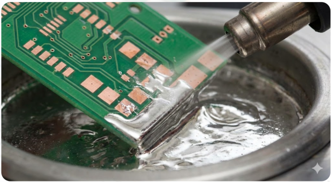
In case you have ever been confused by seeing the acronym HASL on the PCB spec sheet and wondered what it means, here is the brief description: HASL is the abbreviation of Hot Air Solder Leveling, and it is one of the oldest, and still most dependable, surface finishes in the printed circuit board. You simply put the board into a pot of molten solder, typically a tin-lead or lead-free blend, and blow hot air over the solder to remove the excess and leaving a thin coat of solder on each exposed copper pad.
Why then do we have to cover exposed copper? Copper melts as soon as you leave it out: a thin sheet of copper oxide comes up in a few days, and it is a nightmare to solder--you may manage to do it, or you may not at all. HASL provides those pads with a sacrificial shield to keep air and moisture off, and in the process pre-tins all the pads so that you are ready to enjoy an excellent solderability in the future. It is kind of sunscreen on your board, but your solder joints are happier in this case throughout the year.
The resultant HASL finish is solid, easy to examine visually (you can literally see that shiny solder coating), and it wets up well when you are assembling the board. Since ancient times, HASL has been the default of general-purpose boards, fast prototyping, and consumer electronics in large volumes where the price and reliability are superior to the requirement of ultra-fine pitch.
Evolution from Leaded to Lead-Free HASL for Modern Compliance
The initial process of HASL was based on the eutectic tin-lead (Sn63/Pb37) solder alloy, melting at a comfortable 183 o C to form extremely smooth and bright finishes. This has been the gold standard in years. Next was the RoHS directive of the European Union in 2006 and lead became persona non grata in the majority of consumer electronics.
Use lead-free HASL, in which the tin-lead alloy is substituted with other alloys such as SAC305 (tin-silver-copper) or tin-copper alloys. The alloys are more difficult to melt (about 217 to 227 o C), which implies that the process requires a closer thermal control and more careful air knife calibration. The resultant surface is somewhat less planar than conventional leaded HASL- a trade-off that is acceptable with small-scale parts but is not at all objectionable to regular SMD and through-hole designs.
The good news? New fabrication plants such as JLCPCB have invested in state-of-the-art lead free HASL lines that yield exceptionally repeatable results. The leaded to lead-free conversion was not smooth, but the industry has grown up to the extent that currently lead-free HASL is the default offering when it comes to making HASL PCBs that are compliant.
Pro-Tip: If your design uses components with pitch finer than 0.5mm, consider whether the slight surface unevenness of lead-free HASL might cause bridging. For most standard designs, though, lead-free HASL remains the most cost-effective compliant option.
HASL vs. ENIG: A Practical Comparison for Designers
Cost, Shelf Life, and Planarity Advantages of HASL
ENIG vs HASL debate is technically one of the most prevalent debates in PCB design forums - as these two finishes literally control the market. We can deconstruct the places of HASL victory. The obvious huge benefit is cost. HASL is significantly cheaper than ENIG (Electroless Nickel Immersion Gold), typically by 30-50 percent based on the complexity and volume of the board. The HASL raw materials (mainly tin based solder) are significantly cheaper than nickel silver chemistry used in ENIG. In cost-sensitive applications, particularly in consumer electronics and hobby builds, this price difference may literally be the difference between success and failure.
Another HASL strength is shelf life. High quality HASL finish can remain solderable up to 12 months or longer in case you store it well. ENIG also has a very good shelf life, but HASL can do this without the chance of developing black pad syndrome a nickel corrosion defect peculiar to ENIG that can lead to disastrous failures of solder joints. Where HASL is weak in comparison with ENIG is planarity. Hot-air leveling process automatically produces a somewhat domed solder mask on pads that would not be optimal with fine-pitch BGAs or QFN packages which require a perfectly flat landing. ENIG has a thin and uniform layer of gold and provides a flatter surface.
When ENIG Outperforms HASL in High-Reliability Applications
ENIG is especially a big deal when you require ultra-flat surfaces, wire-bonding and long-term contact durability. It is commonly used in medical equipment, space equipment, and high-frequency radio frequency boards since nickel barrier prevents copper diffusion and the gold plating ensures that solder connections remain solid despite months of shelf life. ENIG is essentially the only viable choice when it comes to applications using the aluminum wire bonding such as the majority of semiconductor packaging. HASL simply cannot provide you with the correct surface on which you can form a bond. Moreover, in a harsh environment where the board has to work in extreme temperatures with temperature swings, the more predictable intermetallic growth of ENIG is a huge scorecard over the thicker and less uniform solder layer in HASL.
Real-World Scenarios Favoring HASL in Volume Production
This is where HASL is most useful: high-volume production with standard-pitch parts (0.65mm - and larger), through-hole components, and standard SMD components. Consider consumer electronics, IoT sensor boards, LED lighting controllers, power supplies, and industrial control boards, all that fits. At volumes of thousands or tens of thousands boards per month and where your BOM does not contain ultra-fine-pitch packages, you can save you considerable money without any degradation of reliability when you use HASL instead of ENIG. Many customers of JLCPCB discovered that converting their ENIG-based production boards to lead-free HASL reduces the unit cost per unit, and that the process does not reduce the first-pass yields when assembling a product.
The Professional HASL Application Process
Fluxing, Tinning, and Precise Hot Air Leveling Steps
Frankly, HASL is extremely easy, it is only a matter of dipping, blowing, and you are through, however, the performance of the true professionals requires a plethora of carefully synchronized actions. The fabricated PCB is then subjected to complete cleaning and pre-treatment such that the copper surfaces are free of oxides, oils and other contaminants. This is followed by a flux coating that is used to ensure that the solder becomes wet and prevents re-oxidation in the tinning process. The board is then immersed in a bath of molten solder maintained at exactly regulated temperatures (typically 250-260°C for lead-free alloys).
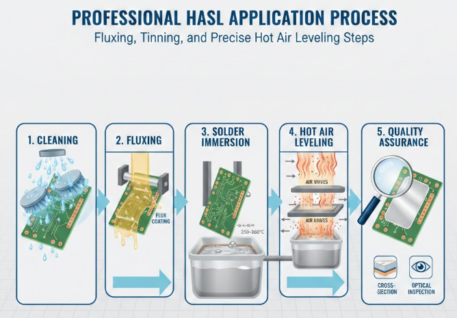
The most important stage is the hot-air leveling. Both sides of the board are blasted with high pressure air knives, clearing the excess solder as the board is pulled out of the bath. The rate of withdrawal, air pressure, air temperature, and the gap between the knife are factors which contribute to the ultimate coating thickness and uniformity. Excessive pressure will cause solder to be stripped off the small pads; excessive pressure will cause thick uneven deposits. Finding that equilibrium is the key between professional fabrication and mere amateur efforts.
Thickness Control and Uniformity in Industrial Lines
Typical Fines of prof HASL lines are 1 to 25 mu, industry sweet spot is approximately 2-15 mu. It requires a lot of high-tech equipment with lots of adjustable knobs to get the same thickness across an entire panel, particularly when the ground pads are huge and the signal pads are small.
The new vertical HASL machines (which JLCPCB uses) are much more capable of maintaining the thickness even than the older horizontal machines. The solder empties out evenly due to the rotation of the machines and the air knives reach both sides of the board simultaneously and this makes the entire plate a bit more uniform.
Quality Assurance for Solderability and Durability
After HASL is on the boards undergo rigorous QA. Solderability tests (typically IPC J-STD-003) ensure that the finish does in fact wet up once the board is assembled. An optical inspection is performed to identify any irregular coverage, bare copper, non-hazardous bridging, or excessive accumulation. The boards are sometimes made into cross-section slides to ensure that the actual coating thickness is checked and to examine the intermetallic layers. All these measures ensure that at the time when a board comes out of the line it is going to support during the final assembly and work continuously.
Key Benefits of HASL in Reliable PCB Fabrication
Excellent Wettability for Wave and Reflow Soldering
Wicked wettability of HASL is the first reason it has been a success in my projects. Since the surface already contains solder coating, it only desires new solder both during wave and reflow. That pre-tinned finish reduces the possibilities of tombstoning, weak joints, and those irritating non-wetting failures that other finishes continue to produce. In the case of boards containing a mixture of both through-hole and surface-mount components, HASL maintains the same level of solderability in both processes. It is a major victory should you be attempting to achieve the greatest first-pass yield and not have to drag off a million solder drills.
Robust Protection Against Oxidation and Environmental Stress
The solder shell on the board is a hard metal cover that prevents oxidation and other menacing effects of the environment. Compared to OSP, which disintegrates during heat and humidity exposures, HASL remains solid over months during storage. And so when your boards are sitting in stock weeks or months before you put them together, HASL can still hold. It is also really durable to everyday handling. Fingerprints or small scratches or those conditions inherent in a typical warehouse will not ruin its solderability as easily as delicate finishes such as immersion silver or OSP.
Scalability for High-Volume and Cost-Sensitive Projects
The economics of HASL improve with size. They are inexpensive in materials, the dip-and-blow process only requires a few seconds a panel, and the equipment is a fine-tuned, battle-proven product. HASL is the choice when running high volume, and it is most important to save on unit cost. In terms of supply-chain, everything that is compatible with HASL can be found everywhere. You will never find a contract manufacturer who cannot do HASL-finished boards and this will reduce the pain of vendor selection and supply risk.
How JLCPCB Excels in HASL Surface Finish Delivery
Advanced Equipment for Consistent Lead-Free HASL Results
JLCPCB has the best vertical HASL lines which are completely calibrated to lead-free SAC alloys. These machines maintain the coating thickness constant regardless of the density and pad shape of different panels, and so you can rely on the solder spots regardless of the complexity of your board. The modern equipment translates to tight process windows and increased first pass yield, which is a win to all.
Integrated DFM Support to Optimize HASL Compatibility
Prior to the release of your board into production, JLCPCB performs automated DFM checks on your Gerber files to identify possible HASL compatibility problems. They mark issues such as pad-to-pad distance that is too small (poor solder bridging), small thermal reliefs, and other design anomalies that can cause the finish to be disrupted. This preventive strategy will identify trouble at an early stage before it becomes costly production errors to save time and money on revision cycles.
Proven Track Record in Delivering High-Yield HASL Boards
JLCPCB delivers millions of boards annually and has developed its HASL process to provide a good high yield. It does not matter whether you are ordering five prototypes or five thousand production panels, the same strict controls and quality checks are applicable. And that reliability is the reason engineers continue to give a thumbs up, knowing that their boards will be on time, they will fit the specifications and will be available to build.

Frequently Asked Questions (FAQ)
Q. What is HASL, and is it still relevant in modern PCB manufacturing?
HASL (Hot Air Solder Leveling) is a surface finish that coats exposed copper pads with a thin layer of solder alloy. Despite being one of the oldest finishes in the industry, it remains highly relevant due to its excellent solderability.
Q. Is lead-free HASL as reliable as traditional leaded HASL?
Yes. While lead-free HASL requires higher processing temperatures and produces a slightly less planar surface. Modern equipment and refined processes have closed the reliability gap significantly.
Q. When should I choose ENIG over HASL?
Choose ENIG when your design includes fine-pitch BGAs (below 0.5mm pitch), requires wire bonding and demands ultra-flat pad surfaces. For standard designs, HASL offers better value without compromising quality.
Q. Can HASL be used for high-frequency or RF applications?
HASL can be used for moderate-frequency designs, but the variable solder thickness may affect impedance consistency at very high frequencies. For RF applications above a few GHz, immersion silver or ENIG typically provides better signal integrity due to their thinner surface profiles.
Q. How long can HASL-finished boards be stored before assembly?
Properly stored HASL boards (in sealed bags with desiccant, away from heat and humidity) can maintain solderability for 12 months or longer. This is significantly better than OSP finishes, which typically have a shelf life of 6 months or less.
Keep Learning
Conformal Coating in PCB Technology: Benefits, Challenges, and Future Developments
If you're searching for conformal coating, you're likely looking for a reliable way to protect your PCB from moisture, dust, chemicals, or harsh environments. Choosing the right coating directly affects product reliability, performance, and lifespan. In this guide, you'll learn what conformal coating is, the main types available, and how to select the best option for your application. We'll also cover key benefits, application methods (manual, automated, and selective), as well as inspection, rework, ......
Preventing Black Pad Defects: Ensuring Reliable ENIG Finish in Professional PCB Manufacturing
Key Takeaways Black Pad is caused by excessive nickel corrosion during the ENIG immersion gold step, leading to brittle solder joints and hidden BGA/QFN failures. Key prevention methods: tight chemistry control (temperature, pH, time), consistent phosphorus content, and regular bath monitoring. High-reliability alternatives: ENEPIG (lowest risk) or nickel-free finishes like Immersion Silver and OSP. Always source ENIG from manufacturers with strict process controls. Ever get a great-looking board, wor......
Solder Mask Colors: Boost Your PCB Performance, Style & Reliability
Key Takeaways Solder mask color directly impacts AOI accuracy, thermal performance, and PCB reliability — it is not purely cosmetic. Green remains the industry benchmark for the highest manufacturing yields and fastest turnaround at no extra cost. White maximizes light reflection for LED applications, while black offers a premium aesthetic for high-end consumer products. Red and yellow provide superior visual contrast for prototyping, debugging, and safety-critical inspections. JLCPCB offers all seven......
Why Copper Oxidation Matters in PCB Design & How to Prevent It
Key Takeaways Copper oxidation is a critical concern in PCB design that directly impacts solderability, contact resistance, and long-term reliability. By understanding how oxidation forms and damages copper surfaces, designers can effectively prevent it through appropriate surface finishes (such as HASL, ENIG, and OSP), strategic solder mask application, and strict adherence to proper storage and handling practices per IPC-1601 guidelines. Protecting copper from oxidation ensures better assembly yield......
Comparing OSP Plating with Other PCB Surface Finishes
Key Takeaways OSP stands out as a cost-effective, ultra-flat, and environmentally friendly PCB surface finish with excellent solderability for fine-pitch components, making it ideal for high-volume consumer electronics. However, its short shelf life (3–6 months), sensitivity to handling and oxidation, and limited multi-reflow durability require careful storage and process control. When compared to HASL, ENIG, Immersion Silver, and Immersion Tin, OSP offers superior planarity and lower cost but trades ......
Hard Gold PCB Finish: Achieving Exceptional Wear Resistance and Contact Performance
Surface finishes are not all the same thing, and this is obvious beyond mention when you are dealing with parts that are beaten against one another over and over. Hard gold. The most common finish used when PCBs must complete hundreds or even thousands of insert-and-remove operations before going out of service is essentially a hard alloy of gold electroplated over a nickel barrier coating. The prototypical piece of evidence that demonstrates why this is important is the edge connector, otherwise know......