From Membrane Frustration to Custom Mechanical Mastery: Taifur's V3 Full Keyboard Project
9 min
- Project Motivation: Why Move from Membrane to Custom Mechanical?
- Project Specifications & Technical Parameters
- Schematic Design & Matrix Architecture: Starting in EasyEDA
- PCB Layout: Three-Layer Functional Art
- Ordering & Fabrication with JLCPCB: Seamless Execution
- Assembly Journey: From Boards to Typing Experience
- Results & Real-World Experience
- Why JLCPCB for Keyboard Builders?
- FAQ about Taifur's Custom Mechanical Keyboard
Note
- Motivation: Replaced a dust-prone membrane keyboard with a durable, custom DIY alternative.
- Specs: 87-key TKL layout powered by Raspberry Pi Pico (RP2040), featuring hot-swap support, QMK, OLED, and an encoder.
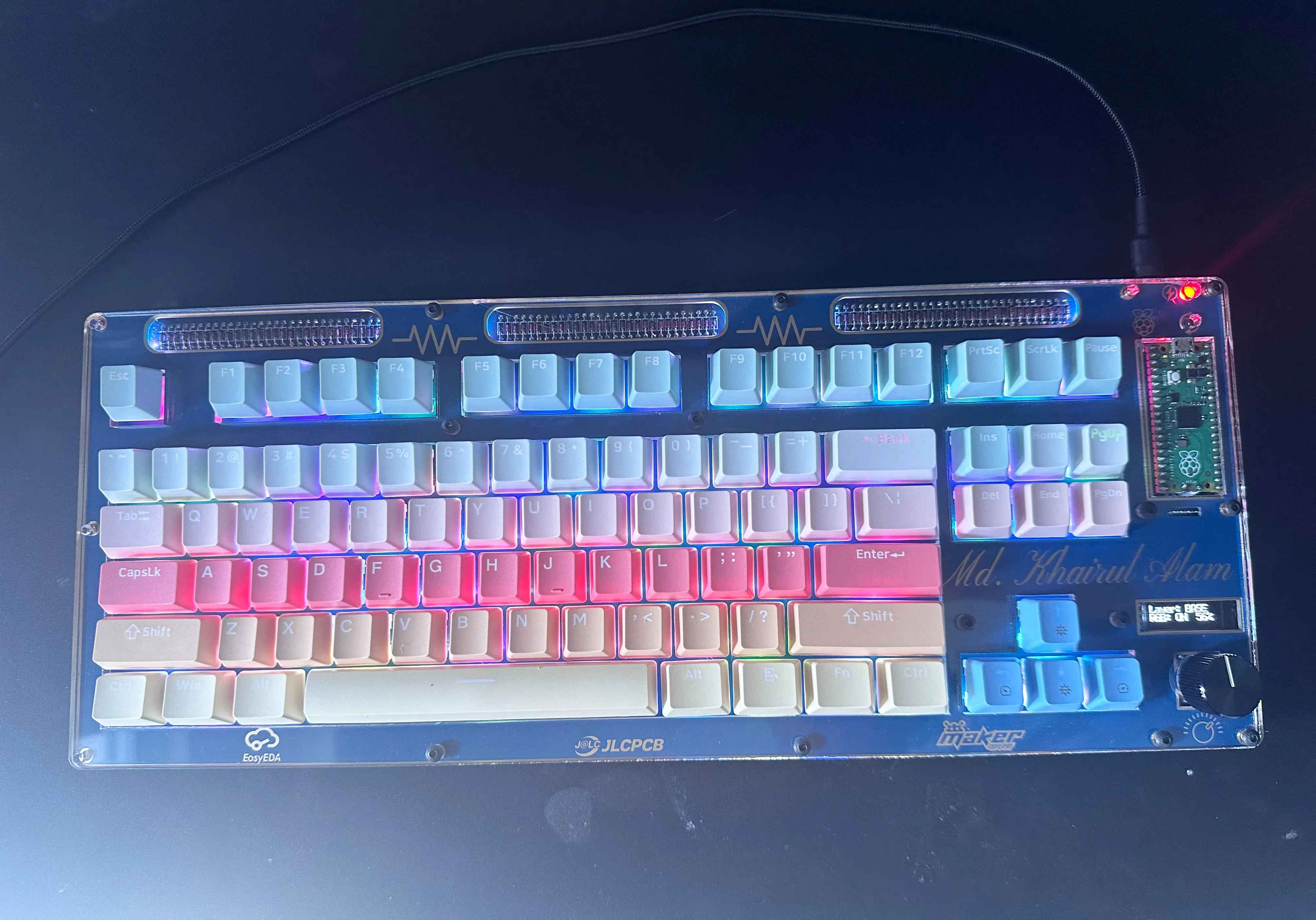
- Design: A unique 3-layer PCB stack featuring symmetrical routing, an exposed controller, and visible "diode art".
- Support: Designed using EasyEDA and fabricated by JLCPcB, the project was submitted to the EasyEDA Spark program successfully securing parts and materials sponsorship for its development.
- Fabrication: Designed in EasyEDA and manufactured via JLCPCB, utilizing SMT assembly to handle the high-density LEDs effortlessly.
In the world of electronics hobbyists and DIY communities, custom mechanical keyboards stand out as one of the most rewarding projects. They combine personalized typing experiences with PCB design, firmware development, and mechanical engineering. Taifur's "Mechanical Keyboard V3 Full" project on OSHWLab is a shining example: a Tenkeyless (TKL) mechanical keyboard featuring a Raspberry Pi Pico (RP2040) controller, full QMK firmware support, per-key RGB lighting, an OLED display, and a rotary encoder.
As a JLCPCB customer, Taifur designed the project in EasyEDA and ordered the multi-layer PCBs through JLCPCB, completing the journey from concept to a fully functional daily driver. This case study explores the project in detail, highlighting how JLCPCB's PCB fabrication and PCBA services helped turn a vision of functional PCB art into reality.
Project Motivation: Why Move from Membrane to Custom Mechanical?
Like many users, Taifur started with standard membrane keyboards. Over time, he noticed performance degradation—stiff, inconsistent, or unresponsive keys caused by dust, debris, and moisture. His desk faces a large window, accelerating dust buildup and forcing him to replace keyboards every few months.
Switching to a mechanical keyboard was a revelation. The distinct feel, sound, and durability sparked deep interest in the community. After researching switches, keycaps, layouts, and DIY projects, he decided to build his own from scratch—not just for personal use, but to share with the maker community that inspired him.
Design Philosophy: Technical reliability + visual symmetry + engineering art. Taifur treated the PCB as a visible design element, focusing on clean trace routing, component symmetry, and aesthetic balance.
Project Specifications & Technical Parameters
The keyboard achieves a strong balance of features, component density, and manufacturability. The table below summarizes the key technical build parameters that supported the design goals and successful fabrication at JLCPCB.
| Parameter | Specification | Benefit / Rationale |
|---|---|---|
| Total Keys | 87 (TKL layout) | Compact yet fully functional for productivity and gaming |
| PCB Layers | 3 separate PCBs (Base + Plate + Frame) | Combines electrical, mechanical support, and aesthetic exposure |
| Total LEDs | 93 (87 per-key + 6 accent) | Rich RGB effects with decorative highlights around diode rows |
| Diodes | 87 (one per key, aligned in 3 rows) | Full NKRO + artistic visual element when backlit |
| Controller | Raspberry Pi Pico (RP2040) | Excellent QMK support and ample GPIO for matrix + peripherals |
| Hot-Swap Support | Yes (all positions) | Easy switch customization without soldering |
| Additional Peripherals | OLED (128×32, I²C), Rotary Encoder, USB Type-C | Enhanced usability with visual feedback and physical controls |
| Board Colors | Black (base), Blue (plate), Purple (frame) | Black maximizes RGB contrast; colored layers add visual depth |
| Typical Board Thickness | 1.6 mm per layer | Standard, rigid, and cost-effective for multi-layer stacking |
| Surface Finish | ENIG (recommended) | Excellent solderability for hot-swap sockets and fine-pitch LEDs |
| Fabrication Turnaround | ~20 days (standard) | Reliable delivery with professional packaging |
This configuration demonstrates efficient use of JLCPCB's standard capabilities while enabling advanced aesthetics and functionality.
Schematic Design & Matrix Architecture: Starting in EasyEDA
While many open-source keyboard projects use KiCad, Taifur chose the familiar EasyEDA platform for faster iteration.
Key Challenges & Solutions:
- Switch Footprint: No ready-made library footprint supported MX-style pads, hot-swap sockets, and proper mechanical cutouts. He customized an existing one for perfect fit and reliability.
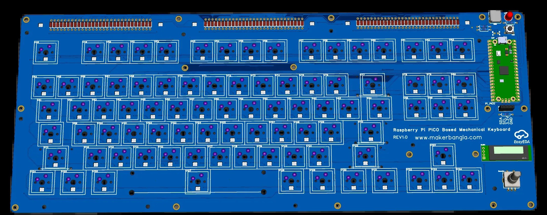
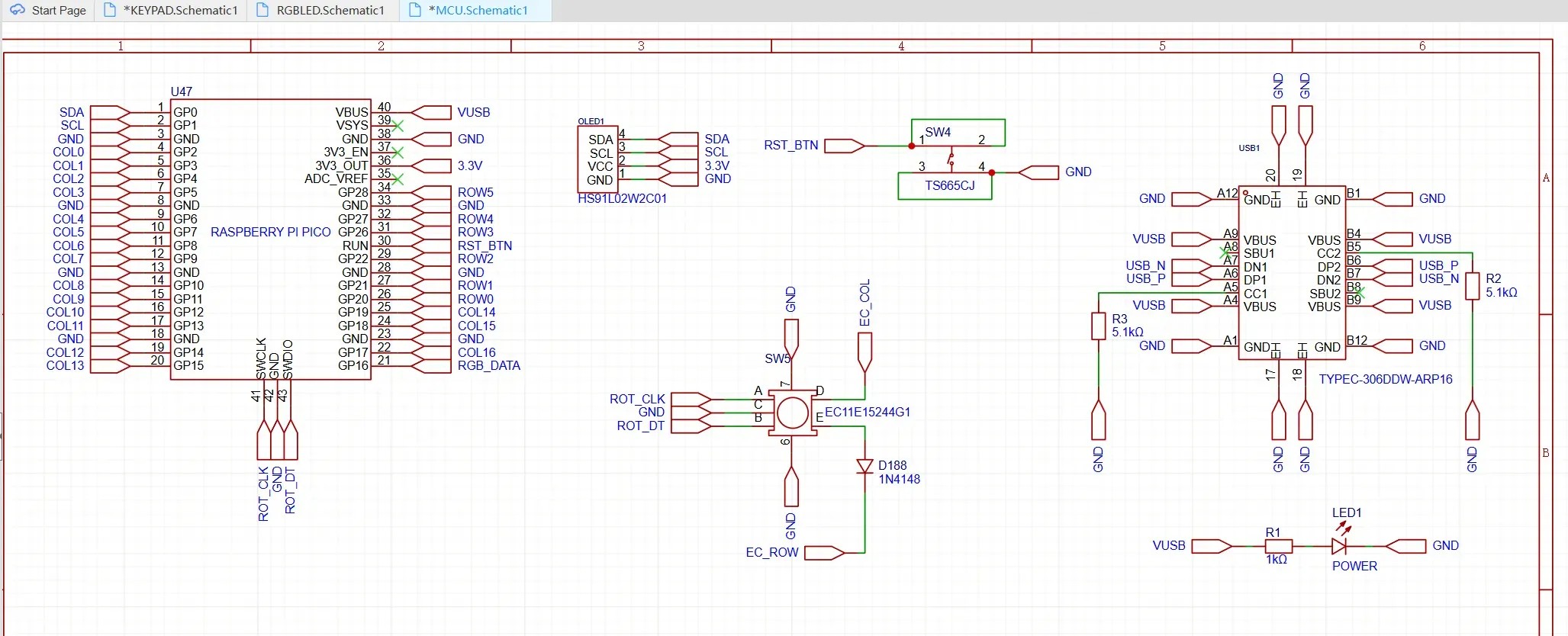
- Key Matrix: 87 keys organized into a 6-row × 14-column matrix to minimize GPIO usage and simplify routing/firmware.
- Anti-Ghosting: One diode per key (column-to-row orientation) for full N-key rollover (NKRO).
- RGB Lighting Circuit: 93 addressable LEDs in a single daisy-chain. 470Ω series resistor on the data line for signal integrity. Multiple decoupling capacitors on the power rail to prevent voltage drops and flickering under full load.
- Peripherals: OLED via I²C (minimal pin usage). Rotary encoder with quadrature pins + push-button integrated into the matrix. USB Type-C wired to Pico for modern, reversible connectivity. Reset button and power LED.
All elements align with JLCPCB's standard capabilities: 2+ layer FR-4 boards, comfortable trace/space rules (typically 6/6 mil or better), and layouts optimized for SMT assembly of hot-swap sockets and fine-pitch LEDs.
PCB Layout: Three-Layer Functional Art
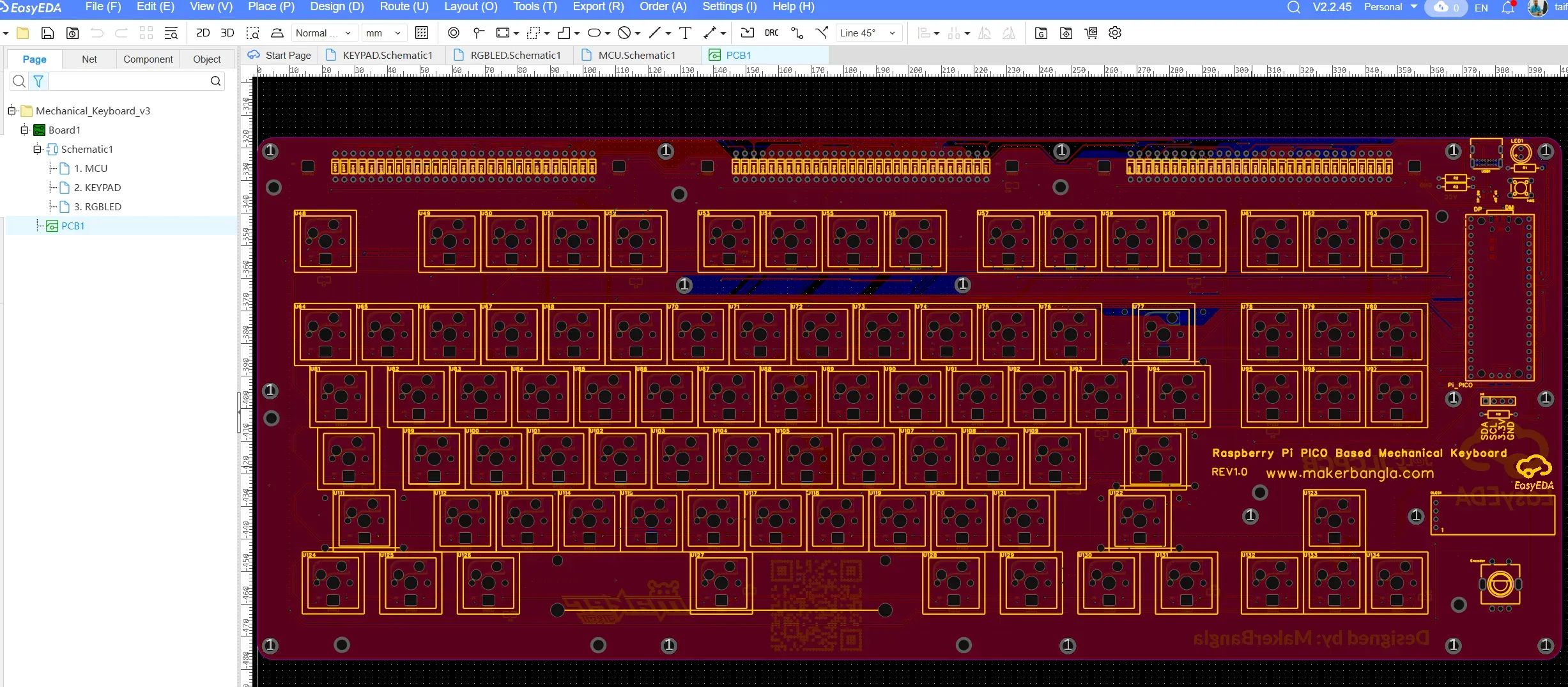
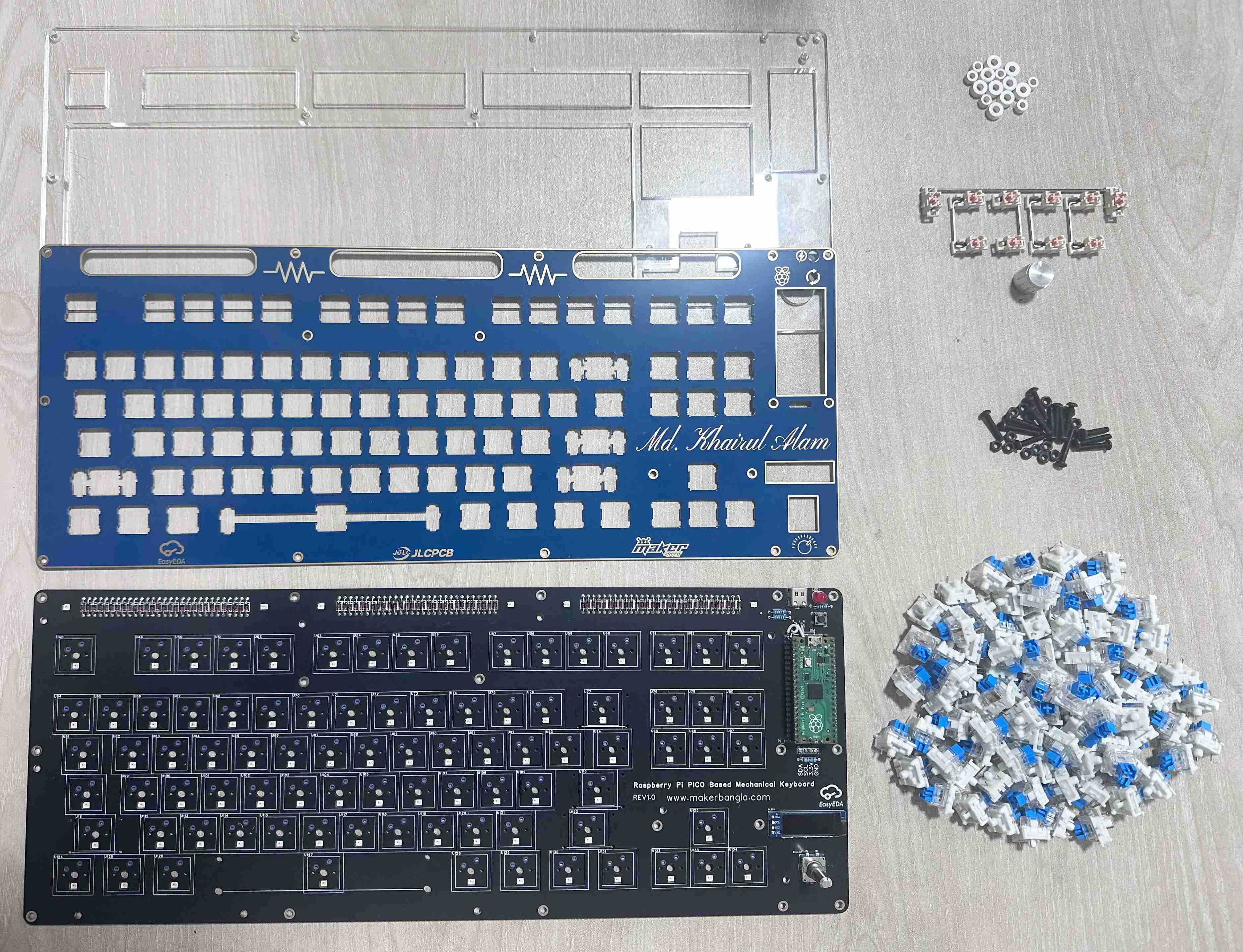
Unlike traditional single-PCB + metal plate designs, Taifur created a three-layer PCB structure where each layer serves electrical, mechanical, and aesthetic purposes:
- Base PCB: Hosts all electronics — hot-swap sockets, diodes, RGB LEDs (bottom-mounted with light cutouts), Pico, OLED, encoder, and Type-C.
- Plate PCB: Provides mechanical switch support with strategic cutouts.
- Frame PCB (optional): Defines shape and rigidity; paired with acrylic top.
Standout Design Features:
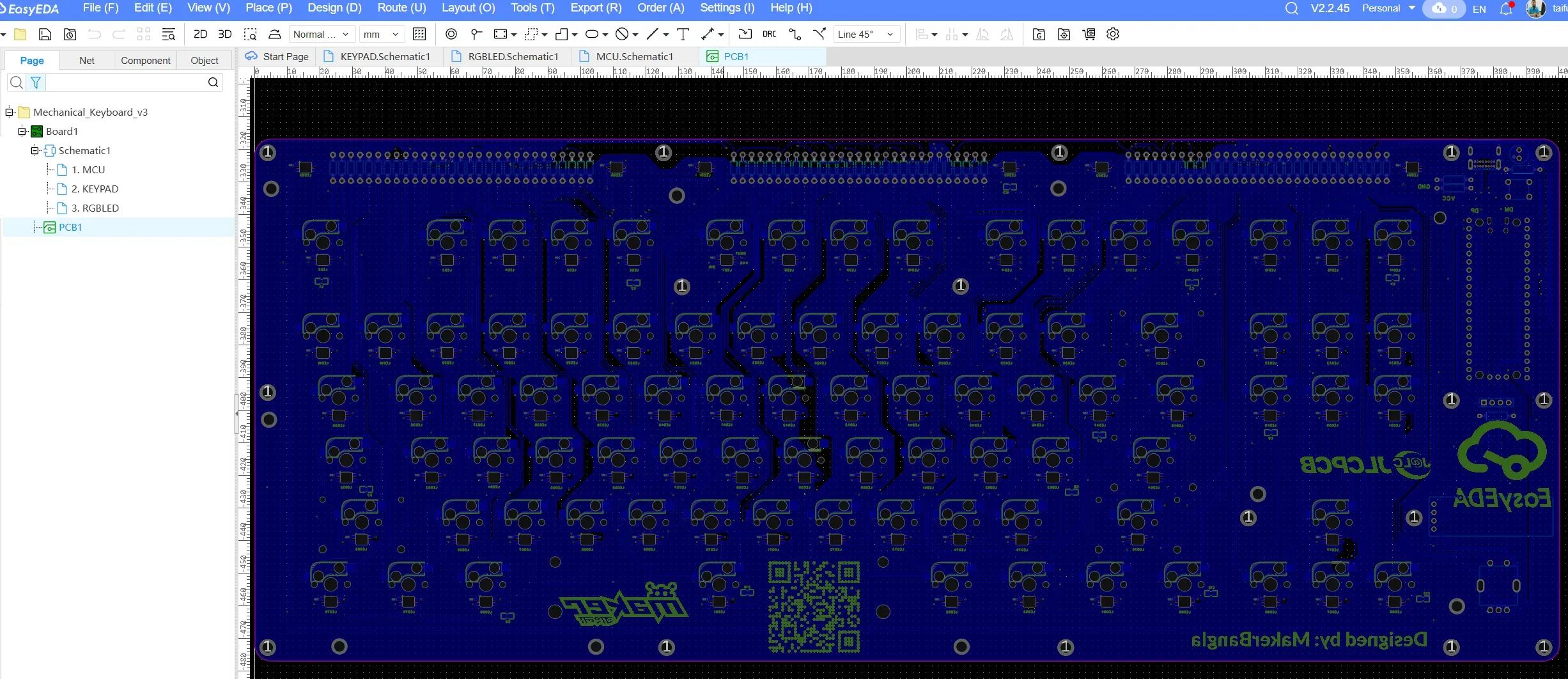
- Diode Art: Diodes aligned into three clean parallel rows instead of scattered placement. Accent RGB LEDs on both sides create striking illuminated frames. Plate and frame windows expose them for visual impact.
- Exposed Controller: Pico mounted visibly on the right side with a matching plate window — celebrating the DIY spirit.
- Precision Workflow: Keyboard Layout Editor (KLE) → SwillKB Plate Builder (DXF export) → EasyEDA for exact switch placement.
- Routing Excellence: Clean, symmetrical traces with careful attention to signal integrity and visual harmony. Bottom-mounted LEDs keep the top surface pristine.
The design strictly adheres to JLCPCB manufacturing rules: standard minimum features, precise multi-layer alignment, recommended ENIG finish for reliable soldering, and black solder mask for enhanced RGB contrast. JLCPCB's capabilities easily support the hot-swap pads, LED cutouts, and complex outlines.
Ordering & Fabrication with JLCPCB: Seamless Execution
After DRC verification in EasyEDA, Taifur ordered directly via the integrated JLCPCB flow. He selected black base boards (for RGB pop), blue plate, purple frame, appropriate thickness, and considered PCBA.
Why JLCPCB Excels Here:
- Integrated Workflow: Gerber, BOM, and CPL files transfer smoothly. In-Stock parts library simplifies sourcing diodes, LEDs, passives, etc.
- Precision Manufacturing: Accurate cutouts, windows, and layer registration.
- PCBA Advantage: Professional SMT handles the high component count (93 LEDs + diodes + connectors), ensuring consistency and saving hours of hand soldering. Double-sided capability is ideal.
After about 20 days, the boards arrived in professional packaging. Quality feedback was excellent: sharp silkscreen, precise soldering, and perfect dimensions.
Assembly Journey: From Boards to Typing Experience
- Solder female headers for the Pico.
- Install M3 spacers and screws to stack layers.
- Mount stabilizers for larger keys.
- Insert hot-swap switches (e.g., Gateron).
- Add acrylic top for protection and aesthetics.
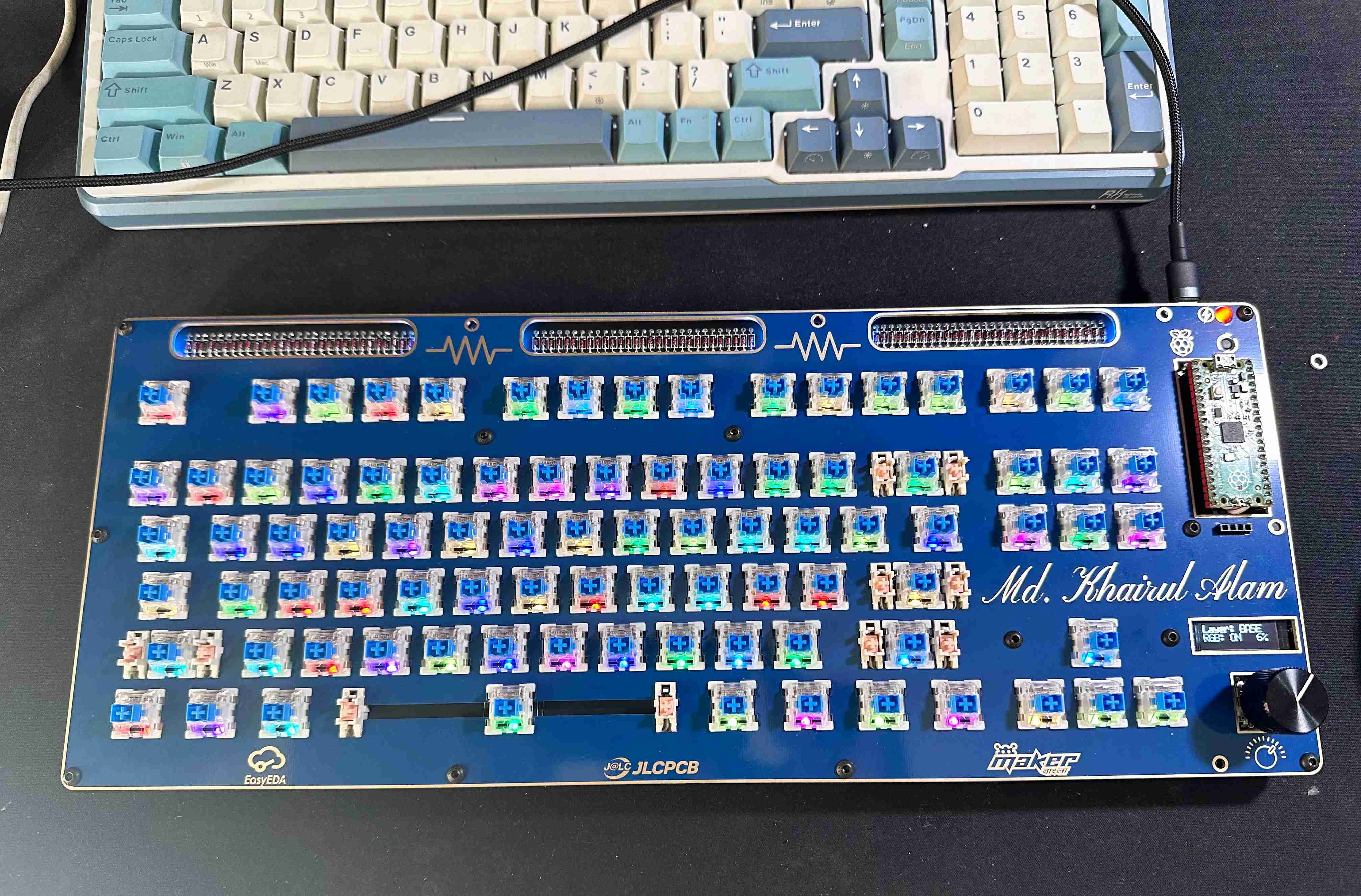
Hot-swap support makes customization effortless. Strategic LED cutouts deliver uniform, beautiful backlighting.
Results & Real-World Experience
The finished keyboard delivers excellent typing feel, vibrant customizable RGB, artistic diode lighting effects, useful OLED feedback, and convenient encoder controls. The exposed design transforms it from a tool into desktop art. Durability in dusty environments far exceeds membrane boards.
Customer Feedback: The project deepened Taifur's PCB design skills and validated JLCPCB's reliability for complex custom builds. The complete hardware-software integration brought immense satisfaction.
Why JLCPCB for Keyboard Builders?
- Rapid prototyping with fast turnaround options.
- Cost-effective small batches and advanced features.
- DFM-friendly tools and documentation reduce errors.
- High-quality SMT for dense designs like per-key RGB.
- Proven track record with countless open-source keyboard projects.
Tips for Similar Projects
- Set DRC according to JLCPCB capabilities early.
- Leverage In-Stock parts for smooth PCBA.
- Consider full assembly service for LED-heavy boards.
- Verify mechanical clearances and lighting paths.
FAQ about Taifur's Custom Mechanical Keyboard
Q: Why choose a Raspberry Pi Pico over a dedicated keyboard MCU?
The RP2040 offers excellent QMK firmware support, ample GPIO pins for large key matrices and peripherals, and an affordable price point. Its dual-core Cortex-M0+ processor handles both matrix scanning and RGB LED control without performance issues, making it a popular choice for DIY keyboard builds.
Q: What is the advantage of a three-layer PCB design?
Separating the base (electronics), plate (mechanical support), and frame (aesthetics/rigidity) into three distinct PCBs allows each layer to be optimized for its function. This approach improves structural rigidity, enables creative visual effects (diode art, exposed controller), and simplifies manufacturing compared to trying to integrate everything into a single board.
Q: Is hot-swap worth it for a custom keyboard?
Yes. Hot-swap sockets allow you to change switches without desoldering, making it easy to experiment with different switch types (linear, tactile, clicky) and customize the typing feel over time. This is especially valuable for first-time builders who are still discovering their preferences.
Q: Can JLCPCB handle complex keyboard PCB designs?
Absolutely. JLCPCB's capabilities easily support the fine-pitch LEDs, hot-swap socket pads, intricate cutouts, multi-layer alignment, and ENIG surface finish required for custom keyboards. The integrated EasyEDA-to-JLCPCB workflow streamlines ordering, and their PCBA service handles high component counts with professional quality.
Q: How long does it take to build a custom mechanical keyboard?
Fabrication typically takes around 20 days with standard JLCPCB service. Assembly time depends on complexity: for a project like Taifur's V3 with PCBA handling most SMT components, final assembly (headers, spacers, switches, stabilizers) can be completed in a few hours. Full hand-soldering of all components would take significantly longer.
Conclusion on Taifur's V3 Keyboard Project
Taifur's Mechanical Keyboard V3 Full demonstrates how thoughtful PCB design can blend technology and art. With JLCPCB's professional fabrication and assembly, makers can confidently bring ambitious ideas to life—whether a TKL keyboard, macro pad, or beyond.
Explore the project files on OSHWLab, download Gerbers and BOM, and start your own build. Order at JLCPCB and experience the joy of turning pixels into precise, tactile reality.
Explore more about EasyEDA Spark now!

Popular Articles
• PiBrick Pocket-CM5: A Compact Raspberry Pi CM5 Handheld PC Built with JLCPCB
• From Membrane Frustration to Custom Mechanical Mastery: Taifur's V3 Full Keyboard Project
• Turn Your Raspberry Pi Pico into a Professional JTAG Programmer with DirtyJTAG & OpenFPGALoader
• Premium Portable Speaker Built with 8-Layer PCBs, DSP & Smart Amps
• ESP32 Smart Control Board for Realistic RC Model Automation
Keep Learning
Athena: Building a High-Performance 6-Layer PCB for Rocket Avionics
Key Takeaways Athena is an open-source flight computer with a triple-MCU architecture, redundant sensors, and multiple communication interfaces on a compact 6-layer PCB. The 80 × 140 mm board integrates three STM32 MCUs, three IMUs, barometers, GNSS, LoRa, Bluetooth, CAN, USB, flash storage, SD card, and power management. The 6-layer PCB provides routing capacity, organized power distribution, signal organization, and compact functional integration for this complex design. The project demonstrates how......
PiBrick Pocket-CM5: A Compact Raspberry Pi CM5 Handheld PC Built with JLCPCB
Key Takeaways The piBrick Pocket-CM5 is a fully functional, smartphone-sized Raspberry Pi CM5 handheld PC with a physical QWERTY keyboard, AMOLED display, and M.2 NVMe SSD The project utilizes JLCPCB's 4-layer PCB fabrication with controlled impedance (90-ohm for USB, 100-ohm for PCIe/MIPI DSI) to maintain signal integrity Designed using EasyEDA and fabricated by JLCPCB, the project was submitted to the EasyEDA Spark program, successfully securing parts and materials sponsorship for its development. J......
Designing a Precision 72-LED Wearable Watch: Building a 40mm Round PCB with JLCPCB SMT Assembly
Key Takeaways This case study explores the design and fabrication of a 72-LED wearable watch built on a precision 40mm round PCB. Learn how JLCPCB SMT assembly eliminated hand-soldering 70+ 0603 LEDs, how ENIG surface finish ensures reliability in wearable applications, and how a clever panelization strategy with mouse-bite breakaway tabs enabled automated assembly of a circular board. The project demonstrates a complete workflow from EasyEDA schematic capture to firmware optimization and commercial-g......
From Membrane Frustration to Custom Mechanical Mastery: Taifur's V3 Full Keyboard Project
Note Motivation: Replaced a dust-prone membrane keyboard with a durable, custom DIY alternative. Specs: 87-key TKL layout powered by Raspberry Pi Pico (RP2040), featuring hot-swap support, QMK, OLED, and an encoder. Design: A unique 3-layer PCB stack featuring symmetrical routing, an exposed controller, and visible "diode art". Support: Designed using EasyEDA and fabricated by JLCPcB, the project was submitted to the EasyEDA Spark program successfully securing parts and materials sponsorship for its d......
ESP32 Smart Control Board for Realistic RC Model Automation
Key Takeaways This project demonstrates how a well-designed custom PCB, manufactured and assembled through JLCPCB, can democratize advanced electronics for hobbyists. Key lessons include: Prioritizing compact, high-density layouts while respecting DFM rules. Leveraging professional SMT assembly for complex boards. Designing with clear labeling and modularity for user-friendliness. Choosing a manufacturing partner whose capabilities match your project's needs for consistent results. Project Overview: B......
Premium Portable Speaker Built with 8-Layer PCBs, DSP & Smart Amps
Project Background and Introduction When you unbox a beautifully crafted portable speaker that delivers rich, room-filling sound with crisp highs, deep bass, and intelligent audio processing, it’s easy to imagine it came from a big-name factory. But behind this elegant Harman/Kardon-inspired design lies the story of an innovative maker who turned a personal passion project into a fully functional, high-performance audio system—entirely prototyped and produced with JLCPCB’s PCB and PCBA services. This ......