
PiBrick Pocket-CM5: A Compact Raspberry Pi CM5 Handheld PC Built with JLCPCB
15 min
- Hardware Architecture and Core Subsystems
- PCB Layout and High-Density Routing Challenges
- JLCPCB Multi-Layer Fabrication and Impedance Control
- SMT Manufacturing and Fine-Pitch Assembly Execution
- Supply Chain Integration with the LCSC Parts Library
- Design for Manufacturing (DFM) Optimizations
- Modular Interconnection via Flex PCBs
- Mechanical Integration and Housing Enclosure
- FAQ about PiBrick Pocket-CM5 Case Study
- Summary of Manufacturing Success
Key Takeaways
- The piBrick Pocket-CM5 is a fully functional, smartphone-sized Raspberry Pi CM5 handheld PC with a physical QWERTY keyboard, AMOLED display, and M.2 NVMe SSD
- The project utilizes JLCPCB's 4-layer PCB fabrication with controlled impedance (90-ohm for USB, 100-ohm for PCIe/MIPI DSI) to maintain signal integrity
- Designed using EasyEDA and fabricated by JLCPCB, the project was submitted to the EasyEDA Spark program, successfully securing parts and materials sponsorship for its development.
- JLCPCB's automated SMT assembly service handles the challenging 0.4mm pitch board-to-board connectors with laser-cut stencils, vision-guided pick-and-place, and AOI quality checks
- Flexible Printed Circuits from JLCPCB enable complex internal routing within the compact enclosure while maintaining connector stability via polyimide stiffeners
- The entire component sourcing is streamlined through the LCSC Parts Library, reducing procurement delays and assembly costs
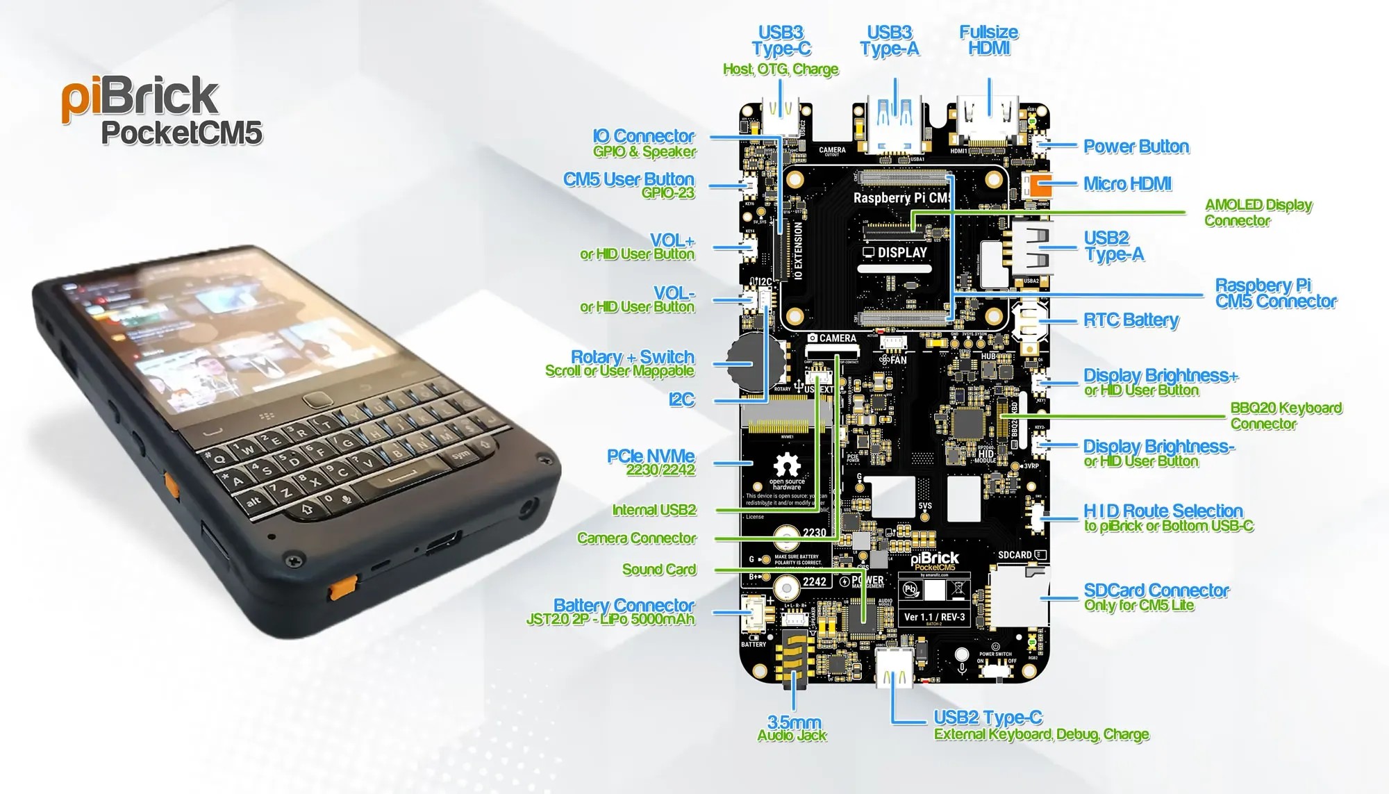
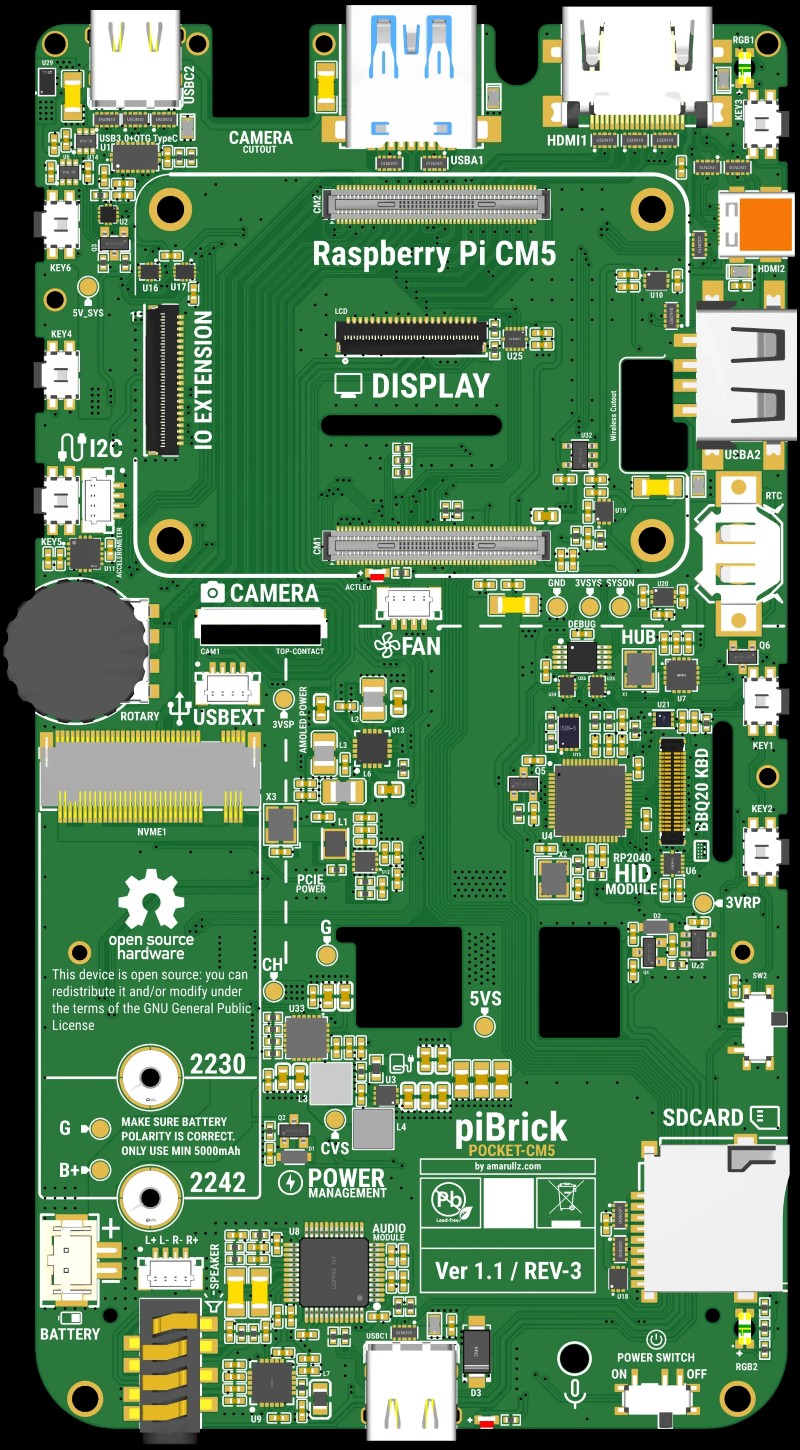
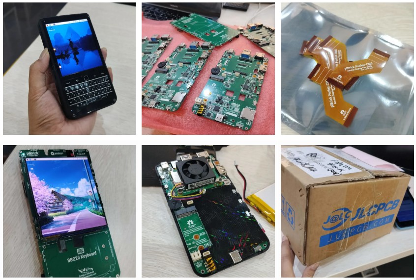
The open-source hardware community has seen a significant shift toward highly integrated, portable computing devices. A standout project in this domain is the piBrick Pocket-CM5, designed by hardware developer Ahmad Amarullah (known as @amarullz on OSHWLab). The project introduces a custom, smartphone-sized carrier board designed specifically for the Raspberry Pi Compute Module 5 (CM5). It allows users to build a fully functional, handheld Linux terminal complete with a physical QWERTY keyboard, an AMOLED display, an M.2 NVMe SSD slot, and a comprehensive power management system.
Bringing a high-density compute module carrier board from a digital schematic to a physical, working device requires highly reliable manufacturing. Because the CM5 breaks out its dense multi-core processor and high-speed I/O interfaces through fine-pitch board-to-board connectors, traditional hand-soldering is out of the question. To achieve the precision necessary for this layout, the developer utilized JLCPCB's turnkey PCB fabrication and Surface Mount Technology (SMT) assembly services.
Hardware Architecture and Core Subsystems
The piBrick Pocket-CM5 is engineered to act as a versatile handheld terminal for system administrators, network engineers, or open-source enthusiasts. To fit this extensive functionality into a compact handheld form factor, the component selection and mechanical placement had to be tightly coordinated.
| Subsystem | Hardware Component | Key Specifications |
|---|---|---|
| Compute Engine | Raspberry Pi CM5 | Multi-core ARM processor, flexible RAM options, native PCIe support |
| Display Panel | 3.92-inch AMOLED | 1080×1240 resolution, 90Hz refresh rate, MIPI DSI interface |
| Primary Input | BlackBerry Q20 Assembly | Full hardware QWERTY layout, integrated optical trackpad |
| Secondary Input | Rotary Encoder + 5 Side Buttons | Tactile navigation, user-definable macro mapping |
| Storage Expansion | M.2 NVMe Slot | Supports 2230 and 2242 form-factor solid-state drives |
| Power Management | Onboard PMIC Architecture | Balanced charging for 5000mAh LiPo battery, multi-rail safety protections |
Desktop-Class Computing Core
The heart of the system is the Raspberry Pi Compute Module 5 (CM5). This System-on-Module (SoM) houses the primary Broadcom processor, RAM, and essential power-regulation chips. By separating the core computing processing unit from the main I/O board, the designer was able to focus entirely on routing peripheral connections on the carrier board, maximizing structural space. The CM5 delivers full desktop-class multi-core performance, allowing the terminal to run native Linux environments like Raspberry Pi OS for on-site diagnostics, server administration, and programming.
Advanced Visual Display Interface
The device utilizes a premium 3.92-inch AMOLED display panel featuring a native resolution of 1080×1240 pixels and supporting a 90Hz refresh rate. AMOLED technology provides exceptional contrast ratios, wide viewing angles, and high power efficiency when displaying terminal interfaces with deep black backgrounds. Capable of driving up to 560 nits of peak brightness for visibility in varying environmental conditions, this display interfaces with the carrier board via high-bandwidth MIPI DSI lanes. This arrangement demands rigorous signal routing to ensure that the high-refresh-rate video signal remains stable and free from electromagnetic interference.
Tactical Human-Machine Interfaces
Unlike typical touch-only mobile devices, the piBrick relies on robust physical input methods to ensure accuracy during intensive terminal operations. It integrates a physical BlackBerry Q20 QWERTY hardware keyboard assembly, allowing users to type terminal commands easily, alongside the original BlackBerry optical trackpad for fine cursor selection. To supplement the keyboard, the carrier board integrates a side-mounted incremental rotary encoder with an embedded push switch, alongside 5 individual tactile physical push-buttons for macro execution and custom system hotkeys.
PCB Layout and High-Density Routing Challenges
The primary challenge of the piBrick Pocket-CM5 project lies in its extreme component density. The overall dimensions of the PCB are restricted by the ergonomics of a handheld device. Within this small footprint, the designer had to route hundreds of traces connecting the CM5's dual high-density 100-pin connectors to various high-speed peripherals.
High-Density Component Positioning
Every square millimeter of the carrier board is utilized. The dual 100-pin connectors form the mechanical and electrical core on one side, while the M.2 NVMe SSD slot, power distribution networks, and audio amplifiers occupy the remaining space. Placing 0402-sized passive filtering components in ultra-close proximity to the high-density ICs was mandatory to decouple electrical noise effectively. This compact arrangement left very narrow corridors for trace escape routing, requiring a careful balance between manufacturing clearance limitations and trace density.
Signal Integrity and Differential Trace Design
When dealing with the high frequencies generated by the Raspberry Pi CM5, signal integrity becomes a primary design concern. The board must handle several high-speed differential pairs simultaneously, which are highly sensitive to layout geometry:
- MIPI DSI Lines: These lines require precise length-matching between the positive and negative traces of each pair to avoid skew, which causes phase shifts and display artifacts.
- PCIe Gen 3 Lanes: Running to the NVMe storage, these lines operate at gigahertz speeds, making them highly sensitive to impedance mismatches. Any unexpected trace geometry deviation, tight 90-degree bend, or unnecessary layer transition (via) introduces signal reflections. These reflections can degrade data packets, resulting in reduced read/write speeds, data corruption, or system instability during heavy storage operations.
JLCPCB Multi-Layer Fabrication and Impedance Control
To satisfy the strict signal integrity requirements of the piBrick Pocket-CM5, the designer opted for a 4-layer PCB structure. JLCPCB's standard multi-layer manufacturing capabilities align directly with the structural requirements of this layout.
Controlled Impedance on the JLC04161H-7628 Stackup
For this 4-layer board, the designer relied on JLCPCB's pre-configured JLC04161H-7628 stackup with a standard overall board thickness of 1.6mm. This stackup defines exact thicknesses for the outer copper layers, internal cores, and prepreg bonding materials. Because the dielectric constant of the FR4 material is stable, the designer calculated trace widths and spacing parameters to achieve target characteristic impedances. Specifically, the traces were matched to 90-ohm for the differential USB lines and 100-ohm for the PCIe and MIPI DSI lines.
Establishing Continuous Reference Ground Planes
In a 4-layer configuration, Layer 1 (Top) and Layer 4 (Bottom) serve as primary signal and component placement layers. Layer 2 is established as a solid, uninterrupted Ground Plane, while Layer 3 serves as the Power Plane. The solid copper on Layer 2 ensures that the return currents of the differential signals flow directly beneath the forward signals, minimizing the loop area. This configuration isolates high-speed digital noise from the sensitive analog audio and power charging sections, keeping overall electromagnetic interference (EMI) exceptionally low.
| Layer Number | Layer Name | Material Type | Thickness | Copper Weight | Primary Engineering Purpose |
|---|---|---|---|---|---|
| Layer 1 | Top Layer | Copper / Plating | 0.035mm | 1 oz | Top signal routing, fine-pitch SMT component pads |
| Inter-layer | Prepreg | FR4 (7628) | 0.2104mm | N/A | High-voltage dielectric isolation, impedance reference |
| Layer 2 | Internal Plain 1 | Copper | 0.0175mm | 0.5 oz | Solid ground reference plane for high-speed signals |
| Core Layer | Internal Core | FR4 | 1.065mm | N/A | Central mechanical core backbone of the PCB structure |
| Layer 3 | Internal Plain 2 | Copper | 0.0175mm | 0.5 oz | Primary power distribution rails and voltage planes |
| Inter-layer | Prepreg | FR4 (7628) | 0.2104mm | N/A | Dielectric separation layer for bottom impedance matching |
| Layer 4 | Bottom Layer | Copper / Plating | 0.035mm | 1 oz | Bottom signal routing, additional component placement |
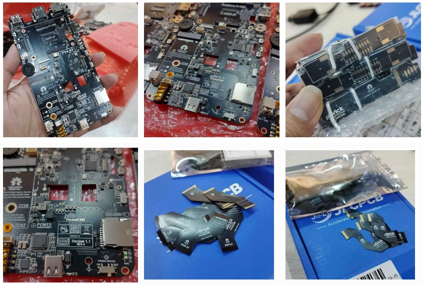
SMT Manufacturing and Fine-Pitch Assembly Execution
The most critical step in physicalizing the piBrick Pocket-CM5 is the soldering of its surface-mount components. The board features several advanced packages, including the dual 100-pin board-to-board connectors for the CM5, which feature a tiny 0.4mm pin pitch. Hand-soldering these pins manually is highly inefficient and carries a high risk of creating solder bridges or cold joints.
Step-by-Step SMT Factory Pipeline
- Laser-Cut Stencil Generation: To assemble the 0.4mm pitch connectors successfully, JLCPCB utilizes laser-cut SMT stencils with engineered aperture optimizations. For fine-pitch components, the stencil openings are modified with precise area ratios and smooth wall geometries to ensure a clean, consistent release of solder paste onto the PCB pads. This prevents excessive paste deposition, which is the root cause of solder bridging during the reflow process.
- Vision-Guided Pick-and-Place: The component placement is handled by high-speed, automated pick-and-place machines equipped with optical alignment systems. The machine registers the board's physical fiducial markers to ensure that the 0.4mm pitch connectors and small 0402 and 0603 passive components are placed exactly on their respective pads.
- Multi-Zone Reflow Profiling: Following placement, the boards pass through a multi-zone reflow oven. The temperature profile is strictly monitored to ensure even heating across the entire board, allowing the solder paste to melt uniformly, wet the component leads, and solidify without inducing structural defects like component tombstoning.
- Quality Assurance via AOI: Post-reflow, every board undergoes Automated Optical Inspection (AOI). The system scans the assembled boards at high speed, comparing them against the design data to check for common assembly defects, such as missing components, misalignment, solder voids, or solder bridges. This guarantees that the fine-pitch connections under the CM5 module are structurally sound before shipping.
Supply Chain Integration with the LCSC Parts Library
Sourcing components for complex designs can often lead to delays, especially when dealing with specialized connectors or specific power management ICs. The piBrick Pocket-CM5 project streamlined this process by sourcing components directly through JLCPCB's integrated LCSC Parts Library.
The design utilizes the high-density 100-pin, 0.4mm pitch board-to-board female sockets (such as the HCTL HC-PBB40C-100DS-0.4V-2.5-02, available under LCSC Part Number C19089280). Because this part is tracked in the JLCPCB assembly database, the pick-and-place machinery is already calibrated for its specific dimensions and packaging constraints, removing the need for manual setup adjustments.
Furthermore, auxiliary resistors, capacitors, and inductors were selected from JLCPCB's "Basic Parts" and "Standard Parts" catalog. Sourcing these standard passives straight from the warehouse means the production run doesn't depend on external third-party part distributors. This reduces the need for custom parts sourcing, lowers assembly costs, and minimizes overall production lead times.
Design for Manufacturing (DFM) Optimizations
To ensure a smooth manufacturing run without delays, the piBrick design incorporates several practical Design for Manufacturing (DFM) details that comply with JLCPCB's production standards.
- Invisible Tracking Barcode Placement: Every PCB processed through an automated assembly line requires a unique 2D tracking barcode. To prevent this barcode from being printed randomly over functional components or exposed copper pads, the developer utilized JLCPCB's "Specify Position" feature. A dedicated 5×5 mm rectangular frame was added to the silkscreen layer underneath where the CM5 module sits, keeping the visible areas of the board clean.
- Tolerance Controls and Clearance Rules: Traces and copper pours maintain a safe distance from the physical outer edges of the PCB to ensure that mechanical routing and panel separation do not clip active lines. Via sizes are chosen within standard drilling limits, preventing breakout issues between the drill hole and its surrounding annular ring on internal layers.
- Minimum Trace Thresholds: The board layout respects reliable manufacturing thresholds, maintaining a minimum trace width and spacing threshold of 3.5 mil to ensure absolute trace structural integrity during the chemical etching process.
Modular Interconnection via Flex PCBs
Because the piBrick Pocket-CM5 is a compact handheld device, it requires sub-assemblies—such as the display interface and peripheral buttons—to sit on different planes within the mechanical enclosure. Standard rigid PCBs cannot bend to fit these spaces, and traditional wiring harnesses are too bulky. To solve this, the project incorporates custom Flexible Printed Circuits (Flex PCBs) manufactured by JLCPCB.
JLCPCB's Flex PCB fabrication line uses a high-quality polyimide base material, allowing for ultra-thin, flexible circuits that can route high-density signals through tight curves. Polyimide provides excellent thermal stability during assembly and retains its mechanical properties under repetitive flexing, ensuring long-term interconnect reliability inside the terminal enclosure.
While flexibility is required to route traces around internal obstructions, the connection points require stability. The custom Flex cables include integrated polyimide stiffeners applied directly behind the exposed gold fingers. These stiffeners increase the thickness of the FPC at the insertion ends, matching the mechanical specification of the ZIF/FFC connectors on the main board. This prevents the flexible substrate from buckling or backing out during final system assembly.
Mechanical Integration and Housing Enclosure
A high-density electronics project is only complete when safely housed in its mechanical shell. The piBrick Pocket-CM5 features a multi-part, custom-designed enclosure optimized for 3D printing.
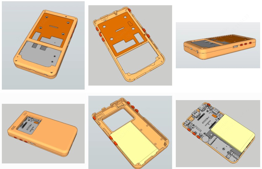
The mechanical housing features precise cutouts to accommodate the rich array of external physical I/O ports. Because the component selection was constrained by strict dimensional limits, the physical orientation of the connectors matches the spacing of the shell's apertures perfectly. The design maps clean cutouts for:
- Twin external USB Type-C data and power ports
- Micro-HDMI display outputs for external monitors
- A spring-loaded MicroSD card expansion slot
- Dedicated physical paths for the side button arrays and the rotary encoder shaft
Because the PCB dimensions and component heights were strictly adhered to during the SMT assembly process, the assembled mainboard slides perfectly into the internal mounting bosses of the enclosure. The alignment between the physical connectors and the printed case openings matches up smoothly, giving the final open-source device a solid, structurally sound, and unified feel.
FAQ about PiBrick Pocket-CM5 Case Study
Q: What is the core processor used in the piBrick Pocket-CM5 and what operating system does it run?
The device is powered by the Raspberry Pi Compute Module 5 (CM5) and natively runs full Linux distributions, such as Raspberry Pi OS, to serve as a handheld workstation.
Q: Why does this project require a 4-layer PCB design instead of a standard 2-layer board?
The 4-layer structure provides dedicated internal power and ground planes. This layer configuration is necessary to manage controlled impedance (90 ohms for USB and 100 ohms for PCIe/MIPI DSI) and preserve high-speed signal integrity.
Q: How is the soldering of the ultra-fine 0.4mm pitch board-to-board connectors handled?
Manual soldering is bypassed entirely by using JLCPCB's automated SMT assembly service. The factory utilizes optimized laser-cut stencils and high-speed pick-and-place machines to prevent solder bridging and ensure accurate component alignment.
Q: How are the peripheral modules and the display connected inside the tight enclosure?
They are linked using custom polyimide Flexible Printed Circuits (Flex PCBs) fabricated by JLCPCB. These thin, flexible circuits allow reliable signal routing around tight corners and include built-in mechanical stiffeners for secure connector fitment.
Summary of Manufacturing Success
The piBrick Pocket-CM5 successfully demonstrates how individual developers and hardware teams can design and manufacture complex single-board computer carrier boards. By utilizing EasyEDA Pro for schematic and layout design, sourcing components through the LCSC Parts Library, and manufacturing the multi-layer boards via JLCPCB's high-density SMT assembly service, the project moves from concept to physical reality without the roadblocks typically associated with advanced prototyping.
The automated application of solder paste via optimized stencils, high-speed pick-and-place component registration, and rigid multi-layer impedance control ensure that the fine-pitch interfaces required by the Raspberry Pi CM5 perform reliably. This integrated manufacturing model provides a predictable, repeatable path for anyone looking to build, iterate, or replicate advanced open-source computing hardware.
If you're passionate about open source hardware and eager to get involved in innovative projects, learn about OsHWLab stars. Join us and work with a global community of makers to bring your ideas to life!
Explore more about the OSHWLab stars now!

Popular Articles
• Turn Your Raspberry Pi Pico into a Professional JTAG Programmer with DirtyJTAG & OpenFPGALoader
• Premium Portable Speaker Built with 8-Layer PCBs, DSP & Smart Amps
• ESP32 Smart Control Board for Realistic RC Model Automation
• PiBrick Pocket-CM5: A Compact Raspberry Pi CM5 Handheld PC Built with JLCPCB
Keep Learning
From Membrane Frustration to Custom Mechanical Mastery: Taifur's V3 Full Keyboard Project
In the world of electronics hobbyists and DIY communities, custom mechanical keyboards stand out as one of the most rewarding projects. They combine personalized typing experiences with PCB design, firmware development, and mechanical engineering. Taifur's "Mechanical Keyboard V3 Full" project on OSHWLab is a shining example: a Tenkeyless (TKL) mechanical keyboard featuring a Raspberry Pi Pico (RP2040) controller, full QMK firmware support, per-key RGB lighting, an OLED display, and a rotary encoder. ......
PiBrick Pocket-CM5: A Compact Raspberry Pi CM5 Handheld PC Built with JLCPCB
Key Takeaways The piBrick Pocket-CM5 is a fully functional, smartphone-sized Raspberry Pi CM5 handheld PC with a physical QWERTY keyboard, AMOLED display, and M.2 NVMe SSD The project utilizes JLCPCB's 4-layer PCB fabrication with controlled impedance (90-ohm for USB, 100-ohm for PCIe/MIPI DSI) to maintain signal integrity Designed using EasyEDA and fabricated by JLCPCB, the project was submitted to the EasyEDA Spark program, successfully securing parts and materials sponsorship for its development. J......
ESP32 Smart Control Board for Realistic RC Model Automation
Key Takeaways This project demonstrates how a well-designed custom PCB, manufactured and assembled through JLCPCB, can democratize advanced electronics for hobbyists. Key lessons include: Prioritizing compact, high-density layouts while respecting DFM rules. Leveraging professional SMT assembly for complex boards. Designing with clear labeling and modularity for user-friendliness. Choosing a manufacturing partner whose capabilities match your project's needs for consistent results. Project Overview: B......
Premium Portable Speaker Built with 8-Layer PCBs, DSP & Smart Amps
Project Background and Introduction When you unbox a beautifully crafted portable speaker that delivers rich, room-filling sound with crisp highs, deep bass, and intelligent audio processing, it’s easy to imagine it came from a big-name factory. But behind this elegant Harman/Kardon-inspired design lies the story of an innovative maker who turned a personal passion project into a fully functional, high-performance audio system—entirely prototyped and produced with JLCPCB’s PCB and PCBA services. This ......
Turn Your Raspberry Pi Pico into a Professional JTAG Programmer with DirtyJTAG & OpenFPGALoader
In the world of FPGA development, having a reliable, low-cost JTAG programmer used to mean either buying expensive vendor cables or adding high-cost FTDI chips to every board. Maker Khaled Magdy changed that by turning a $4 Raspberry Pi Pico into a fully functional JTAG adapter using DirtyJTAG firmware and OpenFPGALoader — then had his custom FPGA boards professionally assembled by JLCPCB. The entire solution is 100% open-source. You can download the firmware, follow the Windows installation steps, an......
Build a Professional 8x8 RGB LED Matrix with JLCPCB
In the world of DIY electronics, building a clean, reliable 8×8 RGB LED matrix used to mean hours of painstaking hand-soldering — 64 WS2812B LEDs plus 64 decoupling capacitors. That all changed when maker Lucas Fernando designed a fully custom PCB from scratch and had it professionally assembled by JLCPCB on his very first try. The result? Five perfectly finished, ready-to-use 8×8 addressable LED matrices that look like commercial products. Best of all, the entire project is 100% open-source. You can ......