Athena: Building a High-Performance 6-Layer PCB for Rocket Avionics
12 min
- Project Highlights
- Why Athena Uses a 6-Layer PCB
- A Triple-MCU Architecture for Distributed Processing
- Redundant Sensors for a More Capable Flight Computer
- Power Management Within the 6-Layer PCB
- Multiple Communication Interfaces on One PCB
- From Design Challenges to PCB Manufacturing Requirements
- From PCB Design to Manufactured Hardware
- Bringing an Open-Source Flight Computer to Life
- What This Project Demonstrates
- FAQ about Athena 6-Layer PCB
- Conclusion on Athena 6-Layer PCB
Key Takeaways
- Athena is an open-source flight computer with a triple-MCU architecture, redundant sensors, and multiple communication interfaces on a compact 6-layer PCB.
- The 80 × 140 mm board integrates three STM32 MCUs, three IMUs, barometers, GNSS, LoRa, Bluetooth, CAN, USB, flash storage, SD card, and power management.
- The 6-layer PCB provides routing capacity, organized power distribution, signal organization, and compact functional integration for this complex design.
- The project demonstrates how open-source hardware can transition from design to manufactured hardware with professional PCB manufacturing and assembly services.
Advanced rocketry requires a flight computer to bring together processing, sensing, communication, power management, and control within a compact and reliable hardware platform. Athena, an open-source flight computer project by NotARoomba, addresses these requirements with a triple-MCU architecture, redundant sensing, multiple communication interfaces, dedicated control channels, and a 6-layer PCB.
The Athena board measures 80 × 140 mm and integrates three STM32 MCUs, three IMUs, barometers, GNSS, LoRa, Bluetooth, CAN, USB, flash storage, an SD card interface, and multiple power-management functions. The project was designed in EasyEDA, with JLCPCB credited for PCB manufacturing and assembly. This case study looks at how the design combines dense functionality with a multilayer PCB architecture and how professional PCB manufacturing supports the transition from an open-source design to physical hardware.
Project Highlights
Athena is a good example of a high-performance embedded PCB in which multiple functional blocks must coexist on a relatively compact board. Rather than treating processing, sensing, communication, power, and control as isolated circuits, the design brings them together into one multilayer platform.
Why Athena Uses a 6-Layer PCB
The Athena project combines three MCUs with multiple sensors, communication modules, storage, power conversion, and dedicated control channels. Accommodating these functions on an 80 × 140 mm board requires more routing capacity and a more organized layer structure than a simple two- or four-layer design would provide.
More Routing Capacity
A 6-layer PCB provides additional routing resources for connecting the three processing units, sensors, communication interfaces, storage devices, and control circuitry. The extra layers help distribute connections across the board instead of forcing every signal onto a small number of crowded routing surfaces. For a design with several digital interfaces and multiple functional blocks, this additional routing capacity is important for keeping connections organized and making the layout more manageable.
Organized Power Distribution
Athena operates from a 7.4–12 V LiPo input while generating regulated 5 V and 3.3 V rails. The design also includes dedicated power-management devices for battery charging, USB-C power delivery, and servo power. A multilayer architecture can provide more structured power distribution and clearer separation between power and signal routing, helping the designer manage the relationships between different functional sections.
Improved Signal Organization
The flight computer contains multiple high-speed digital interfaces and several sensor connections. A multilayer PCB allows signal routing to be organized across more layers while maintaining reference structures between routing regions. This makes it easier to plan signal paths and reduce unnecessary routing congestion as the design grows in complexity.
Compact Functional Integration
The 80 × 140 mm board integrates processing, sensing, communications, storage, power, and control functions in one hardware platform. Using six layers gives the design more freedom to place these functions efficiently while keeping the overall board footprint compact.
JLCPCB supports 6-layer PCB manufacturing for high-density and mixed-signal designs, with options including controlled impedance and Via-in-Pad for applicable designs. These are manufacturing capabilities available for suitable projects; they should not be interpreted as specific processes used by Athena unless confirmed by the project files.
A Triple-MCU Architecture for Distributed Processing
One of Athena's defining features is its triple-MCU architecture. Instead of assigning every task to a single microcontroller, the project separates processing responsibilities across three STM32 devices. This creates a clear functional division between sensor processing, telemetry and storage, and control functions.
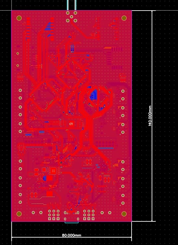
One of Athena's defining features is its triple-MCU architecture.
The MPU handles sensor-related computation and Kalman filtering, while the TPU manages communication and data storage. The SPU is dedicated to pyro and PWM functions. This division places several independent processing blocks on the same PCB, which increases the importance of organized placement and routing.
Athena also provides six pyro channels and six PWM channels, with two PWM channels intended for TVC and four for fin control. These dedicated interfaces add another layer of functional requirements to the PCB layout, because control signals and their associated power and interface circuitry must coexist with the processing and sensing sections.
Redundant Sensors for a More Capable Flight Computer
Reliable flight-control hardware depends on accurate sensing. Athena includes three ICM-45686 IMUs, a LIS2MDLTR magnetometer, and two barometer devices, the ICP-20100 and BMP388. This combination gives the flight computer access to multiple sources of motion, orientation, and atmospheric-pressure information.
Athena Sensor Configuration
- 3 × ICM-45686 IMUs for inertial sensing
- LIS2MDLTR magnetometer
- ICP-20100 and BMP388 barometers
With several sensor devices connected to the processing architecture, the PCB must accommodate multiple signal connections while keeping the sensor area practical for routing and placement. The 6-layer structure gives the designer additional routing resources for these connections and helps integrate the sensing section with the three-MCU processing system.
For a professional PCB manufacturing workflow, the goal is not simply to fit every component onto the board. The layout must also translate into a manufacturable design with appropriate spacing, routing, drilling, and layer construction. JLCPCB's multilayer manufacturing capabilities are designed to support this type of complex PCB architecture.
Power Management Within the 6-Layer PCB
Athena's power system has to support both the flight computer's digital electronics and its control-related functions. The project accepts a 7.4–12 V LiPo input and includes dedicated devices for charging, USB-C PD, servo power conversion, and regulated low-voltage rails.
The presence of several power-management blocks makes power distribution an important part of the PCB architecture. The charger, USB-C power-delivery controller, servo buck converter, and low-voltage regulator each serve different roles, so their placement and interconnection need to be considered together with the rest of the board.
On a multilayer PCB, a structured layer stack can make power and ground distribution easier to organize. JLCPCB offers 6-layer stackups and multilayer fabrication options for designs that require dedicated power and signal-routing structures.
Multiple Communication Interfaces on One PCB
Athena combines several communication technologies on the same flight computer, allowing the platform to communicate with external systems and connect to different onboard functions. The communication section includes GNSS, LoRa, Bluetooth, CAN, USB, and dedicated UART channels.
Integrating these interfaces increases the number of connections that must be routed between modules and the three MCUs. The design therefore benefits from a PCB architecture that provides sufficient routing capacity while maintaining a clear relationship between communication, processing, power, and control sections.
The result is a highly integrated flight computer rather than a collection of separate boards. This type of integration is one reason multilayer PCB manufacturing is commonly used for advanced embedded hardware with many interconnected functions.
From Design Challenges to PCB Manufacturing Requirements
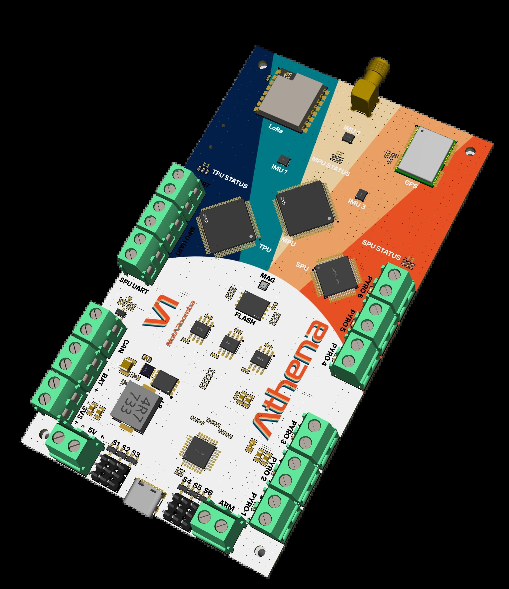
From design challenges to PCB manufacturing requirements.
The table above connects Athena's design characteristics with the manufacturing considerations that commonly accompany a dense multilayer PCB. These are general engineering relationships rather than claims that every listed manufacturing feature was specifically used on Athena.
For an open-source hardware project, manufacturing readiness is especially important because a successful design must move from CAD data to repeatable physical hardware. The PCB manufacturer therefore needs to support the required layer count, materials, fabrication tolerances, and assembly process while maintaining consistency across production.
From PCB Design to Manufactured Hardware
Athena was designed using EasyEDA, while the project credits JLCPCB for PCB manufacturing and assembly. This makes the project a practical example of how an open-source PCB design can progress from schematic and layout work to physical hardware.
6-Layer PCB Manufacturing
JLCPCB supports 6-layer PCB manufacturing with multilayer stackup options suitable for high-density, high-speed, mixed-signal, and other advanced applications. Current 6-layer capabilities include FR-4 constructions, controlled impedance options, and Via-in-Pad processes for applicable designs.
Controlled Impedance and Advanced Interconnect Options
For designs that require tighter signal-integrity control, JLCPCB provides controlled-impedance manufacturing options across supported multilayer constructions. Via-in-Pad is also available for applicable designs, helping designers address routing density around compact component footprints. These capabilities are presented here as JLCPCB manufacturing options and are not claimed as specific features of the Athena board.
PCB Assembly for Integrated Hardware
Once the fabricated board is ready, assembly becomes another important part of bringing a complex flight computer to life. JLCPCB provides PCB assembly services covering SMT and THT requirements across supported board constructions, with inspection capabilities that help support production quality. The exact assembly process depends on the project's component packages, board construction, and production requirements.
Bringing an Open-Source Flight Computer to Life
- Processing: Three STM32 MCUs divide sensor processing, telemetry/storage, and control responsibilities.
- Sensing: Multiple IMUs, a magnetometer, and barometers provide the flight computer with diverse sensor inputs.
- Communication: GNSS, LoRa, Bluetooth, CAN, USB, and UART interfaces connect the system to external and onboard functions.
- Power: Battery charging, USB-C PD, servo power conversion, and regulated rails are integrated into the same PCB.
- Control: Six pyro channels and six PWM channels support dedicated control functions.
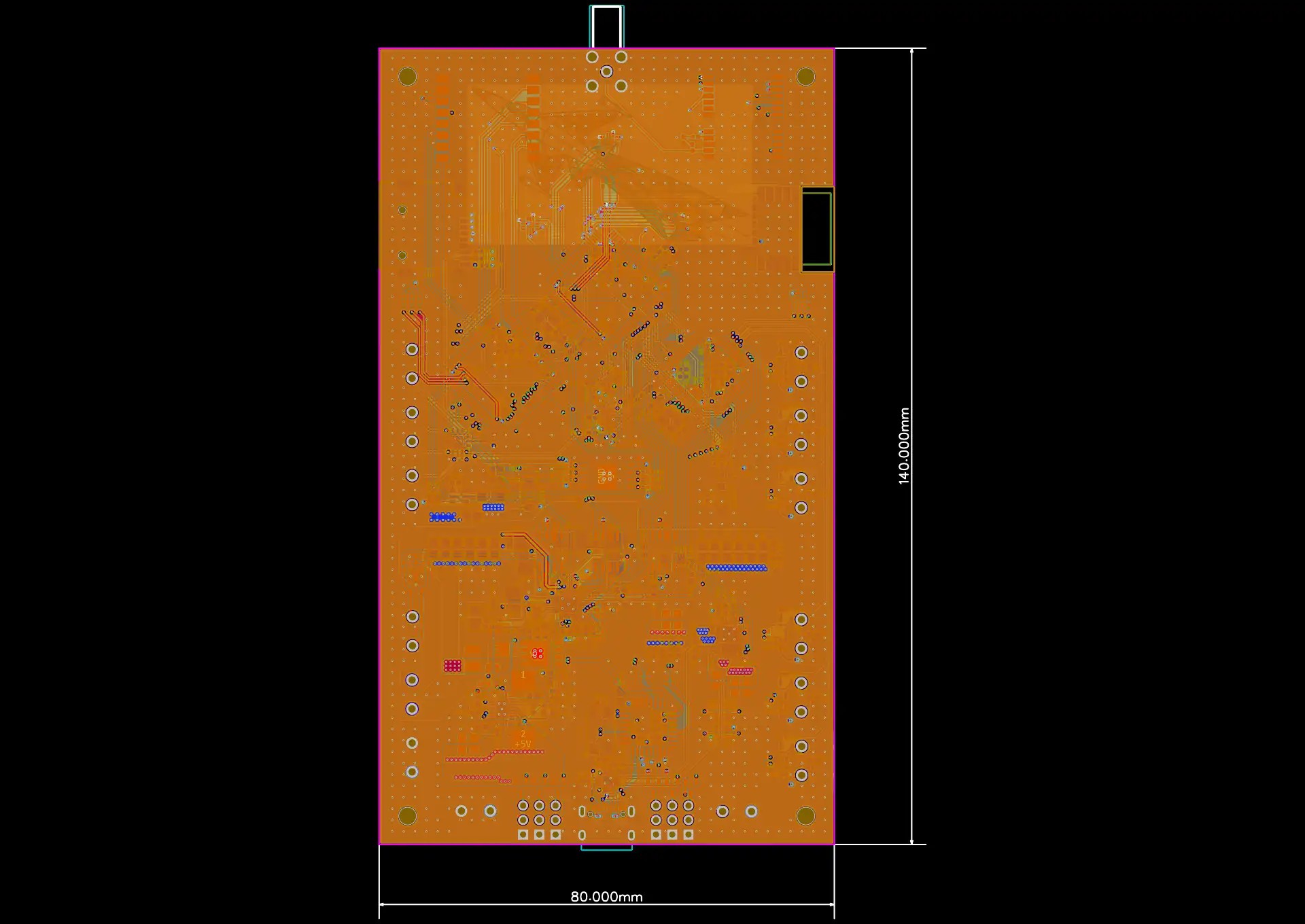
Processing: Three STM32 MCUs divide sensor processing, telemetry/storage, and control responsibilities.
The strength of Athena lies in the integration of these functions. Each block has its own requirements, but the final product must operate as one coordinated flight computer. The 6-layer PCB provides the physical platform that brings these circuits together while maintaining a compact 80 × 140 mm form factor.
What This Project Demonstrates
1. Multilayer PCB Design
Athena demonstrates how a 6-layer PCB can provide the routing and layer-organization resources needed for a complex embedded system. With three MCUs, multiple sensors, communication interfaces, storage, power-management circuits, and control channels, the design illustrates why layer count becomes an important architectural consideration as hardware functionality increases.
2. Functional Integration
Instead of distributing flight functions across several independent boards, Athena integrates processing, sensing, communication, power, and control into one PCB. This approach can simplify the overall hardware architecture while increasing the importance of careful placement, routing, and manufacturing preparation.
3. Hardware Redundancy
The use of multiple IMUs and multiple processing units reflects a design approach that gives different functions dedicated hardware resources. In an advanced embedded system, such architectural separation can help organize computational and control workloads across the board.
4. Manufacturing Readiness
The project credits JLCPCB for manufacturing and assembly, showing the complete path from an open-source EasyEDA design to physical hardware. For complex PCB projects, a capable manufacturing partner is an important part of turning a sophisticated layout into a practical, assembled product.
FAQ about Athena 6-Layer PCB
Q: What is the Athena project?
Athena is an open-source flight computer project by NotARoomba that integrates three STM32 MCUs, multiple sensors, communication interfaces, and power management on a compact 6-layer PCB for advanced rocketry applications.
Q: Why does Athena use a 6-layer PCB instead of 4 layers?
The 6-layer PCB provides additional routing capacity for the triple-MCU architecture, organized power distribution for multiple voltage rails, improved signal organization for high-speed interfaces, and compact functional integration on the 80 × 140 mm board.
Q: What sensors does Athena include?
Athena includes three ICM-45686 IMUs for inertial sensing, a LIS2MDLTR magnetometer, and two barometers (ICP-20100 and BMP388) for atmospheric pressure measurement, providing redundant sensing for reliable flight control.
Q: What communication interfaces are available?
The flight computer integrates GNSS (NEO-M8U-06B), LoRa (RA-02), Bluetooth (DA14531MOD), CAN (TCAN1057AVDRQ1), USB (TUSB2036 hub), and dedicated UART channels with ESD protection for comprehensive connectivity.
Q: How was the Athena board manufactured?
The Athena project was designed in EasyEDA and manufactured by JLCPCB, demonstrating the complete path from open-source design to physical hardware with professional PCB manufacturing and assembly services.
Conclusion on Athena 6-Layer PCB
Athena is a strong example of a high-performance 6-layer PCB designed for an advanced flight-computer application. Its 80 × 140 mm board integrates three STM32 MCUs, multiple sensors, GNSS, LoRa, Bluetooth, CAN, USB, storage, power management, and dedicated pyro and PWM control channels.
The project also demonstrates the value of connecting PCB design decisions with manufacturing requirements. As board functionality and routing density increase, a well-planned multilayer structure and a capable PCB manufacturing and assembly partner become increasingly important. With its 6-layer PCB manufacturing, multilayer fabrication, controlled-impedance options, Via-in-Pad capability, and PCB assembly services, JLCPCB provides manufacturing options that can support a wide range of advanced PCB designs.
If you're passionate about open source hardware and eager to get involved in innovative projects, learn about OsHWLab stars. Join us and work with a global community of makers to bring your ideas to life! Explore more about EasyEDA Spark now!

Popular Articles
• ANGELO Project with JLCPCB: Building an Open-Source Audio PCB for a Listening Aid
• From Membrane Frustration to Custom Mechanical Mastery: Taifur's V3 Full Keyboard Project
• Turn Your Raspberry Pi Pico into a Professional JTAG Programmer with DirtyJTAG & OpenFPGALoader
• PiBrick Pocket-CM5: A Compact Raspberry Pi CM5 Handheld PC Built with JLCPCB
• Premium Portable Speaker Built with 8-Layer PCBs, DSP & Smart Amps
Keep Learning
From Membrane Frustration to Custom Mechanical Mastery: Taifur's V3 Full Keyboard Project
Note Motivation: Replaced a dust-prone membrane keyboard with a durable, custom DIY alternative. Specs: 87-key TKL layout powered by Raspberry Pi Pico (RP2040), featuring hot-swap support, QMK, OLED, and an encoder. Design: A unique 3-layer PCB stack featuring symmetrical routing, an exposed controller, and visible "diode art". Support: Designed using EasyEDA and fabricated by JLCPcB, the project was submitted to the EasyEDA Spark program successfully securing parts and materials sponsorship for its d......
Turn Your Raspberry Pi Pico into a Professional JTAG Programmer with DirtyJTAG & OpenFPGALoader
In the world of FPGA development, having a reliable, low-cost JTAG programmer used to mean either buying expensive vendor cables or adding high-cost FTDI chips to every board. Maker Khaled Magdy changed that by turning a $4 Raspberry Pi Pico into a fully functional JTAG adapter using DirtyJTAG firmware and OpenFPGALoader — then had his custom FPGA boards professionally assembled by JLCPCB. The entire solution is 100% open-source. You can download the firmware, follow the Windows installation steps, an......
ANGELO Project with JLCPCB: Building an Open-Source Audio PCB for a Listening Aid
Key Takeaways Accessible Design: ANGELO is an open-source €10 listening aid created to assist everyday voice amplification. Analog Audio Architecture: Uses a TL072 op-amp to boost speech frequencies (1–4 kHz) with low latency and low power. EasyEDA & JLCPCB Workflow: Designed in EasyEDA and produced via JLCPCB SMT assembly for fast, reliable hardware execution. The ANGELO Project Overview ANGELO is an open-source audio hardware project designed to amplify voices and improve everyday communication expe......
Athena: Building a High-Performance 6-Layer PCB for Rocket Avionics
Key Takeaways Athena is an open-source flight computer with a triple-MCU architecture, redundant sensors, and multiple communication interfaces on a compact 6-layer PCB. The 80 × 140 mm board integrates three STM32 MCUs, three IMUs, barometers, GNSS, LoRa, Bluetooth, CAN, USB, flash storage, SD card, and power management. The 6-layer PCB provides routing capacity, organized power distribution, signal organization, and compact functional integration for this complex design. The project demonstrates how......
PiBrick Pocket-CM5: A Compact Raspberry Pi CM5 Handheld PC Built with JLCPCB
Key Takeaways The piBrick Pocket-CM5 is a fully functional, smartphone-sized Raspberry Pi CM5 handheld PC with a physical QWERTY keyboard, AMOLED display, and M.2 NVMe SSD The project utilizes JLCPCB's 4-layer PCB fabrication with controlled impedance (90-ohm for USB, 100-ohm for PCIe/MIPI DSI) to maintain signal integrity Designed using EasyEDA and fabricated by JLCPCB, the project was submitted to the EasyEDA Spark program, successfully securing parts and materials sponsorship for its development. J......
Designing a Precision 72-LED Wearable Watch: Building a 40mm Round PCB with JLCPCB SMT Assembly
Key Takeaways This case study explores the design and fabrication of a 72-LED wearable watch built on a precision 40mm round PCB. Learn how JLCPCB SMT assembly eliminated hand-soldering 70+ 0603 LEDs, how ENIG surface finish ensures reliability in wearable applications, and how a clever panelization strategy with mouse-bite breakaway tabs enabled automated assembly of a circular board. The project demonstrates a complete workflow from EasyEDA schematic capture to firmware optimization and commercial-g......