
3D AOI Inspection Explained : How It Catches Defects That 2D Systems Miss
12 min
- What Is 3D AOI and Why Does It Matter?
- How 3D AOI Measurement Technology Works
- 2D AOI vs 3D AOI: A Direct Comparison
- Defect Types That Only 3D AOI Can Reliably Catch
- Where Does 3D AOI Fit in the SMT Line?
- Key Benefits Beyond Defect Detection
- How JLCPCB Uses 3D AOI for Consistent Assembly Quality
- FAQ about 3D AOI
- Conclusion
Key Takeaways
3D AOI Inspection has become essential in modern PCB assembly by using advanced height and volume measurement to detect critical solder defects that traditional 2D AOI systems routinely miss, such as lifted leads, insufficient solder, head-in-pillow, and component coplanarity issues. By delivering precise 3D data through structured light or Moire technology, it significantly reduces false calls, improves first-pass yield, and ensures long-term reliability according to IPC-A-610 standards. JLCPCB integrates post-reflow 3D AOI with SPI, X-ray, and functional testing to deliver consistently high-quality SMT assembly for both prototypes and mass production.
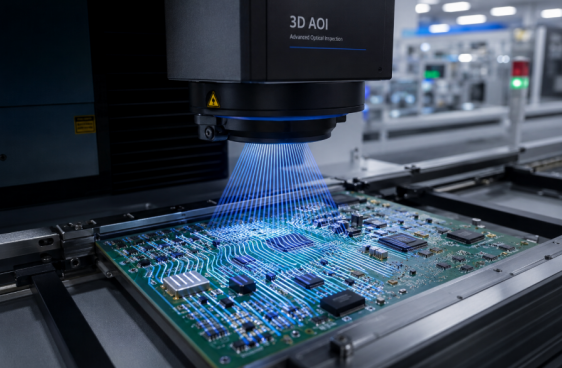
Have you ever realized that a solder joint on a modern PCB is sometimes smaller than a speck of sand, and its quality can mean the difference between a product that lasts for 5 years in the field or fails within 5 months? This is the reason 3D AOI has become the standard for inspection in professional electronics manufacturing. 3D A.O.I. makes invisible defects measurable by accurately capturing the actual height, volume, and shape of each solder joint. The flat camera image is no longer able to distinguish if a joint has enough solder or a lead has lifted off the pad a few microns, especially as packages shrink to 0201 and 01005 size, and BGA pitches get below 0.4 mm.
What you need is depth information, and 3D AOI provides just that. In this article, we will examine the 3D AOI inspection, its measurement technology, its application in the SMT production line, and why it always surpasses the traditional 2D inspection method. We will also explore how JLCPCB applies this technology in their assembly lines, ensuring high-quality production at scale.
What Is 3D AOI and Why Does It Matter?
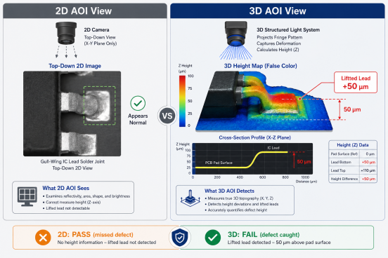
Let's begin at the beginning. The classic method of automated optical inspection (AOI) is based on flat, 2D images taken by cameras that have angled light, and has been around for decades. This is fine for identifying missing pieces or apparent polarity mistakes. However, when it comes to assessing if a solder fillet is of adequate volume or if a gull-wing lead is flat against its pad, a 2D image is not sufficient. 3D AOI inspection addresses this by illuminating the board with a structured light pattern, and an image is captured of the deformation of the pattern over the surface of the components and solder joints. The system produces accurate 3D information at each point, creating a full 3D map of the whole assembly. This is not just a picture. Data measured and compared to metrology grade programmed tolerances based on IPC-A-610 acceptability criteria. Each solder joint receives an objective pass/fail rating, depending on its real geometry, and not just upon the appearance in a picture.
How 3D AOI Measurement Technology Works
But how does a 3D AOI machine obtain three-dimensional information from a flat circuit board? Today, there are three main principles of measurement used in modern systems.
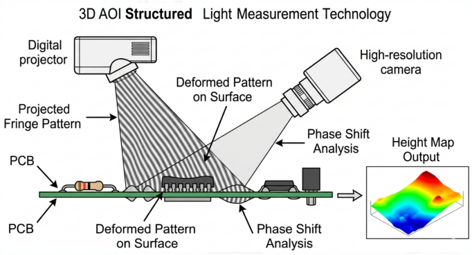
- Phase-shift Moire fringe projection is the most popular method used in high-end 3D AOI systems. Multiple sinusoidal fringe patterns are projected onto the surface of the board by the machine at slightly different phase angles. Each projected pattern is captured by a camera, and the deformation of fringes over the surface features is analyzed. This system can determine the phase shift at each pixel, forming an accurate height map of the whole board.
- Structured light triangulation involves projecting a known geometric pattern onto the board from a projector and capturing that pattern reflected on the board from a camera at a known offset angle. Through the geometric relationship between projected and received patterns, the height information can be obtained by using the triangulation calculation. This approach is fast and is appropriate for inline production.
- The Stereo Moire technique is a method of using two cameras placed in different locations to take pictures of the same fringe pattern being projected at once. The system is able to measure absolute depths, as both cameras measure the same point from different angles, avoiding the 2-pi ambiguity typical of a single-camera Moiré system.
2D AOI vs 3D AOI: A Direct Comparison
If you are wondering whether 3D AOI is truly a significant upgrade over traditional 2D systems, let the numbers speak for themselves.
| Feature | 2D AOI | 3D AOI |
|---|---|---|
| Measurement type | Planar (X, Y only) | Volumetric (X, Y, Z) |
| Solder joint evaluation | Color and shape analysis | Height, volume, and fillet geometry |
| False call rate | Typically 8-10% or higher | Below 5% with optimized programming |
| Lifted lead detection | Unreliable | Accurate height-based detection |
| Coplanarity measurement | Not possible | Standard capability |
| Shadow and reflection sensitivity | High (major source of false calls) | Low (height data eliminates ambiguity) |
| Defect escape rate | 2-5% of real defects | Under 1% for surface-visible defects |
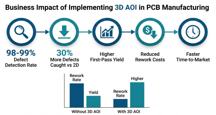
The fundamental issue with 2D AOI is that it is based on brightness thresholds and color analysis for making decisions. In dense layouts, where shadows of high components fall on the neighboring joints, the system will have difficulties discriminating between real defects and optical artifacts. 3D AOI eliminates this entire class of problem. Since it is a physical measurement and not a brightness measurement, a shadow will have no effect on the measurement. Industry benchmarks indicate that 3D AOI is able to detect up to 30% more defects compared to 2D-only inspection.
Defect Types That Only 3D AOI Can Reliably Catch
This is where the true power of 3D AOI becomes apparent. There is a class of solder defects that appear quite normal from the top surface, but from a reliability point of view are totally unacceptable.
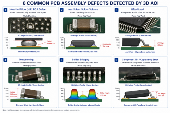
- Head-in-pillow defects: During reflow, the BGA ball partially separates from the solder paste, and the joint is good from the top, but not from the bottom.
- Too little solder volume: This is when there is not enough solder in the joint to create a good fillet. It may be clean in 2D, but it does not have the volume necessary for IPC-A-610 long-term reliability.
- Lifted leads: Gull-wing QFP or J-lead components with a few micrometers of lifted leads. 2D cameras cannot see them, which are easily measurable using Z-axis data.
- Component tilt/coplanarity issues: Passive components or ICs that are placed at an angle that is not within the acceptable range. The only reliable indication is the difference in height between the different sections of the body.
- Tombstoning: One end of a chip component comes off its pad during reflow. Tombstoning can only be observed at the beginning stages by measuring the height.
- Solder bridging with height context: If the soldering is between two adjacent pads, the solder bridge has to be separated by a height context to determine whether the solder bridge is a true bridge or an acceptable solder meniscus.
These defects are too fine to reliably evaluate by 2D evaluation for fine-pitch QFP packages (0.5mm or less), micro-BGA arrays, and miniature 0201 passives.
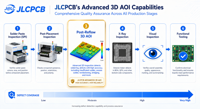
Where Does 3D AOI Fit in the SMT Line?
There are multiple positions for installing a 3D AOI machine in SMT assembly. The functions of each position differ, and where it is best placed will vary with your quality objectives.
- Post-print (SPI position): After the stencil printer, check the solder paste volume, height, and alignment prior to component placement. Here, some 3D AOI machines can be used in addition to dedicated SPI systems.
- Post-placement (pre-reflow): After pick and place, when the presence of all components, correct orientation, and proper seating is confirmed. Preventing reflow of boards with placement errors is a waste of oven time.
- Post-reflow: The most important position. All solder joints are in their final form after the reflow oven. The 3D AOI checks all height-related defect types, wetting, fillet formation, volume, and bridging for each joint.
The best place that 3D AOI pays off is during post-reflow inspection. Modern inline systems work right on the conveyor at line speed and are in real-time communication with upstream equipment. When the system senses a trend (e.g., a decrease in solder volumes on a specific pad pattern), it can alert or stop the line before the issue becomes critical. Smart manufacturers add X-ray inspection to post-reflow 3D AOI for boards using BGA components. While AOI will not be able to see under an opaque package body, X-ray will fill that void for the most complete defect coverage possible.
Key Benefits Beyond Defect Detection
The benefits of 3D AOI systems go far beyond the ability to capture more bad joints. Now, here's what the technology provides throughout the manufacturing process.
- Higher first pass yield: Defects detected right after reflow will not waste other downstream resources.
- Reduced false call rates: Height-based measurements remove shadow and reflection artifacts, leaving operators with much less manual re-inspection.
- Closed-loop process feedback: Volumetric data feeds back in real time to the stencil printer and pick and place machine to allow automatic corrections before defect trends build up.
- Low failure rates in the field: The more that is inspected in the factory, the less will be returned under warranty. It is a "must" for IPC-A-610 Class 3 applications.
- Rapid New Product Introduction: 3D AOI allows engineers to quickly find and solve process problems, speeding up the prototype to production process.
AOI manufacturers that are moving from 2D to 3D routinely report savings of thousands of dollars per production run in rework cost savings alone. This is how JLCPCB applies 3D AOI to ensure quality assembly.
How JLCPCB Uses 3D AOI for Consistent Assembly Quality
So what does all this look like in a production environment? JLCPCB adopts 2D and 3D AOI inspection, which are in-line on the SMT production line. The 3D systems utilize structured light technology to capture obvious solder joint defects, as well as the subtle height-dependent defects that only volumetric inspection can detect, including solder joint height, component coplanarity, and fillet geometry. But 3D AOI is only one step in a multi-step quality assurance process. JLCPCB's full inspection process includes:
- Solder Paste Inspection (SPI): Confirming the volume of solder paste deposited and alignment prior to deposition
- Post-placement verification: Confirmation of the presence, orientation, and seating accuracy of the components
- Post-reflow 3D AOI: Evaluation of all solder joints and component features volumetrically
- X-ray inspection: Dedicated coverage for BGA and hidden-joint packages. Manual checking by trained operators for conditions that are hard for automated systems to determine:
- Functional testing: Powered testing of finished assemblies.
Data from the SPC of the 3D AOI system is displayed on the process control dashboards, allowing solder quality trends to be monitored across all production lines. This thorough inspection system underpins JLCPCB's SMT assembly services, offering engineers a reliable solution for sourcing assembled PCBs, with stencils starting at $6 and competitive assembly prices. The outcome is uniform quality regardless of whether you're placing an order for a few prototypes or tens of thousands of production.
FAQ about 3D AOI
Q: What is 3D AOI, and how does it differ from 2D AOI?
3D AOI uses structured light projection or Moire fringe technology to capture volumetric height data from PCB assemblies. While 2D AOI captures only flat images and relies on brightness analysis, 3D AOI measures the actual height, volume, and shape of each solder joint, enabling the detection of defects like lifted leads and insufficient solder that are invisible to 2D cameras.
Q: Why is 3D AOI better than manual visual inspection?
Manual inspection is subjective, slow, and unable to detect micrometer-level defects on fine-pitch components. A 3D AOI machine provides objective, repeatable measurements against defined tolerances, achieving detection rates above 98% for surface-visible defects.
Q: Can 3D AOI detect every type of assembly defect?
No. 3D AOI excels at surface-visible defects, including solder bridges, tombstoning, lifted leads, and insufficient solder volume. However, it cannot see beneath opaque packages like BGAs. Defects hidden under the package body require X-ray inspection for reliable detection.
Q: Where is the 3D AOI machine placed in the SMT line?
The most common position is post-reflow, after solder joints have reached their final state. Some manufacturers also place systems post-placement to catch component errors before reflow. Post-reflow provides the most comprehensive defect coverage.
Q: How does 3D AOI reduce manufacturing costs?
By catching defects immediately after reflow, 3D AOI prevents defective boards from consuming downstream resources. Lower false call rates reduce wasted re-inspection time, and process feedback data helps correct upstream issues before they produce large batches of defective product.
Conclusion
Today, 3D AOI is considered a must-have for professional PCB assembly. With the continuing decrease in component size and the increase in board density, volumetric measurement is the only method that is reliable to verify solder joint quality at the speed of production. The technology removes whole classes of false calls, offers process data to continually improve, and identifies defects not detectable with flat cameras. Inquire about inspection infrastructure when you assess a PCB assembly partner. With the investment in multi-stage quality assurance, including advanced 3D AOI in the production line, JLCPCB delivers the level of inspection that modern electronic products require.
Keep Learning
Solder Joint Inspection in PCB Manufacturing : A Complete Guide to Catching Defects Early
Key Takeaways Solder Joint Inspection is critical in modern PCB manufacturing to catch defects early and ensure product reliability. By combining Solder Paste Inspection (SPI), 3D AOI for visible joints, and X-ray for hidden BGA/QFN issues, manufacturers can effectively detect common defects such as bridging, cold joints, tombstoning, and head-in-pillow. Following IPC-A-610 standards with a layered inspection strategy significantly reduces field failures while improving first-pass yield. JLCPCB’s prof......
3D AOI Inspection Explained : How It Catches Defects That 2D Systems Miss
Key Takeaways 3D AOI Inspection has become essential in modern PCB assembly by using advanced height and volume measurement to detect critical solder defects that traditional 2D AOI systems routinely miss, such as lifted leads, insufficient solder, head-in-pillow, and component coplanarity issues. By delivering precise 3D data through structured light or Moire technology, it significantly reduces false calls, improves first-pass yield, and ensures long-term reliability according to IPC-A-610 standards......
How Sustainable Materials and Expert Manufacturing Ensure RoHS Compliant PCBs
Have you ever experienced that a finished shipment of products was detained at the EU customs due to a single component on the board not passing the RoHS screening? It is higher than most engineers think, and the financial blow is far bigger than the impounded goods. Wasted time, remodeling expenses, and a compliance audit that is capable of halting your whole product introduction, that is the actual cost of doing RoHS wrong. The point is as follows: RoHS-compliant PCBs cease to be a checkbox exercise......
Preventing PCB Warping: Best Practices for Design and Manufacturing
In the design and manufacturing process of electronic equipment, PCB (Printed Circuit Board) warpage is a common but troublesome problem. PCB warping not only affects the performance and reliability of the device but can also cause connectivity issues and other serious consequences. Therefore, it is crucial to understand how to prevent and resolve PCB warping. This article will explore some best practices in design and manufacturing to help you effectively prevent PCB warpage problems from occurring. ......
PCB Cleanliness in Professional Manufacturing : Preventing Contamination and Ensuring Long-Term Reliability
In the construction of PCBs, the boards are contaminated with all sorts of dirt at almost every stage. In the soldering process, the flux (either rosin-based or more recent organic forms) may cause residues or ionic salts to remain on the pads and traces and be sticky. Next there is etching, plating and micro-etching; the chemical processes will put metal ions on the copper unless the rinsing is complete. Tiny particles of metal shavings, fiberglass dust, and laminate fragments are also thrown out in ......
PCB Basics 5: PCB Testing and Quality Assurance
Welcome to the realm of PCB testing and quality assurance! Quality control is always a crucial part of different industries. Great quality control not only could generate more energy for customers’ electronic projects, but it could also embark on certification and guarantee to the electronic industry. Let’s learn the importance of testing and quality assurance in PCB manufacturing. The Significance of Testing and Quality Assurance in PCB Manufacturing: Testing and quality assurance are extremely impor......