
Mouse Bites in PCBs: Easy Solutions for Clean Separation and Professional Results
13 min
- Understanding Mouse Bites and Their Role in PCB Panelization
- Design Best Practices for Effective Mouse Bites
- Manufacturing Techniques for Reliable Mouse Bites
- Common Issues and Professional Solutions
- JLCPCB's Expertise in Mouse Bite Fabrication
- Frequently Asked Questions (FAQ)
Have you ever broken a PCB off its manufacturing panel and experienced that embarrassing jolt of cringewave when you realized you were left with the rough jagged edge? You see, when you have already handled some panelized boards in our lab, you realise that the de-paneling can make or break the ultimate product. The little rows of holes drilled along breakaway tabs, which people refer to as mouse bites on PCBs, are one of the most efficient methods of separating boards in a very clean way, and learning to do them correctly is more of a science than a gamble.
In such a small project as a microcontroller board based on CH32V003, with a size of just 34.9mm x 17.9mm, every millimeter of edge space matters. Incorrectly placed tabs may cause interference with USB connectors, programming pads, or GPIO headers, and an improperly designed perforation pattern may leave the solder joints cracked, copper chipped, or simply too difficult to break. We are going to take you through all the information you should know about mouse-bite design of PCB panelization, including the placement and geometry, as well as manufacturing accuracy, and the pitfalls to avoid that have bedeviled most of us. Today, we will walk through everything you need to know about mouse bite design for PCB panelization, from placement and geometry to manufacturing precision and common pitfalls. Let's get into it.
Understanding Mouse Bites and Their Role in PCB Panelization
What Mouse Bites Are and How They Work
Mouse bites are a series of small, closely spaced drilled holes typically 0.5 mm to 0.6 mm in diameter and arranged in a line along a breakaway tab that connects individual PCBs to each other or to the surrounding panel frame. The mechanical principle is straightforward: the overlapping perforations create a controlled weak section in the tab material. After assembly is complete, you snap the board free along this perforation line, much like tearing a sheet of stamps from a booklet. Each tab is formed during the routing stage. The CNC router cuts the board outline but leaves narrow bridges, usually 2 mm to 5 mm wide.
The mouse bite drill pattern is then placed along these bridges, creating a panel that is rigid enough for SMT pick-and-place and reflow, yet weak enough to separate cleanly with moderate hand pressure or simple tooling. The relationship between tab routing and mouse bite drilling is critical. The routed slot defines the board outline, while the perforations define the fracture path. If these two features are misaligned, you get uneven breaks or stress that propagates into the board edge.
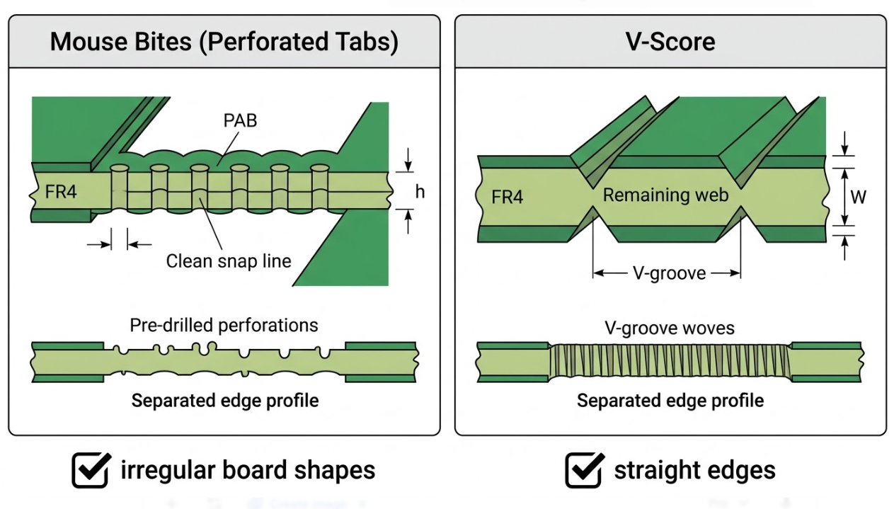
Why They Are Preferred Over Other Depanelization Methods
V-scoring is the most frequently used alternative, with a blade scratching a groove along the top and bottom of the panel in a straight line. V-scoring is good when the board is a rectangle with straight sides, but inaccurate when the outline is irregular or when the sides are crowded with connectors. The benefits associated with mouse bites include:
- They support non-linear and curved board outlines since tabs may be located anywhere on the perimeter.
- They present reduced complexity in tooling to prototype and small-to-medium production, because standard drill bits can cut the perforations without dedicated scoring blades.
- They provide local tab strength during SMT reflow while still allowing easy hand or plier separation afterward.
- Tabs can be positioned strategically to avoid connectors and edge-mounted components.
For a board like the CH32V003 design, which has a USB connector on one edge and programming pads along another, mouse bites let you place tabs only where they will not interfere with functional interfaces. A V-score running along the full edge would cut right through those areas.
Design Best Practices for Effective Mouse Bites
Optimal Placement, Size, and Spacing Guidelines
The first principle is straightforward: place the tabs in mechanically safe edges and avoid them from contacting delicate parts and connectors. In the case of the CH32V003 board (34.9mm by 17.9mm), this would be avoiding the USB connector edge and the programming/reset access edge. Rather, two or three tabs along the longer sides where nothing is rising close to the border.
Here are the key dimensional guidelines for effective mouse bite design:
1.I will turn the drill in the 0.5-0.6mm scale; as long as it is not too thin, then the tab will not bend enough, and as long as it is not too wide, it might break before we even get it to the market.
2.The holes should be spaced 0.7-0.8mm, center-to-center. That is so they are practically touching, and you save the additional metal.
3.Use 5-8 holes per tab, depending on its width. A 3mm tab will typically burn through with 5, whereas a 5mm tab burns through with 7-8.
4.Always leave at least 0.30 to 0.50mm between the last hole and any copper mate trace, pour, or whatever is on the board side.
5.Additionally, maintain a 1.5mm keep-out distance between the tab edge and the nearest component or solder pad.
Integration with Panel Layout and Tab Routing
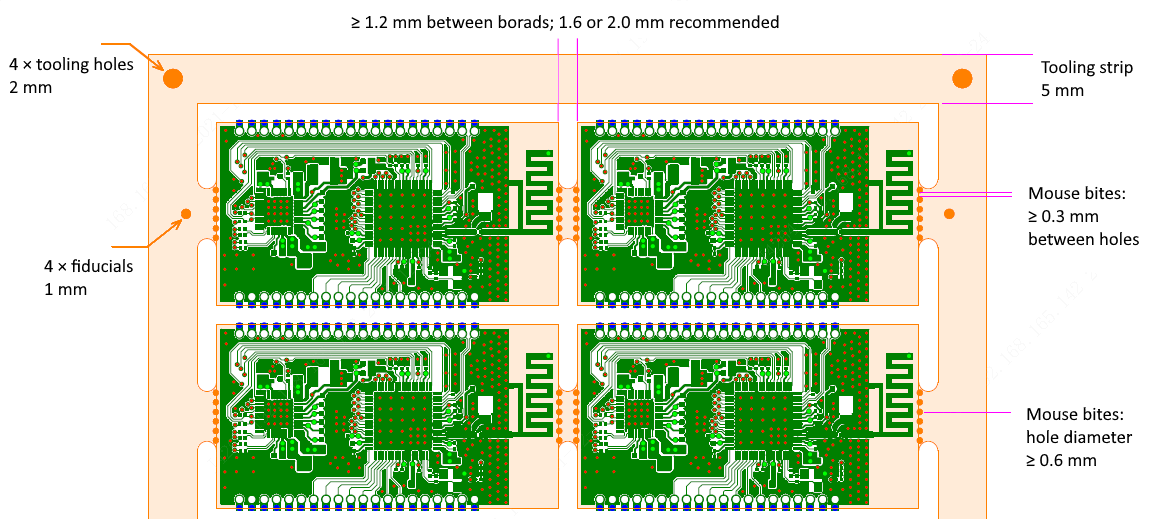
Mouse bites are part of a larger panelization system that includes the routed board outline, panel frame (rails), fiducials, and tooling holes. Treat the tab-route outline and the mouse bite perforation as a single integrated feature, not as two separate design steps.
For a small board like the CH32V003, two tabs per board are often sufficient for a panel of 6 to 10 units. Three tabs provide extra rigidity for double-sided reflow. More than three tabs on a board this size makes depanelization unnecessarily difficult. The table below summarizes recommended tab configurations based on board size:
| Board Longest Edge | Recommended Tabs | Tab Width | Holes per Tab |
| < 25 mm | 2 | 2 - 3 mm | 4 - 5 |
| 25 - 50 mm | 2 - 3 | 3 - 4 mm | 5 - 6 |
| 50 - 100 mm | 3 - 4 | 3 - 5 mm | 5 - 8 |
| > 100 mm | 4 - 6 | 4 - 5 mm | 6 - 8 |
For the CH32V003 board at roughly 35 mm on its longest edge, two to three tabs with 3 mm width and 5 to 6 holes each is the sweet spot. Position these tabs on the two longer edges, away from the USB connector and programming header. This preserves full access to functional interfaces even while the board is still in the panel -- useful for in-panel programming or functional test before depanelization.
Manufacturing Techniques for Reliable Mouse Bites
Precision Drilling and Perforation Control
The entire quality of a mouse bite pattern, frankly speaking, is determined by the precision with which the drilling is done. The two factors are dominating, and they include: consistency of the drill diameter and alignment of the holes with the routed tab contour. The slightest movement of the bit by 0.1 mm off its programmed position causes the perforation line to shift and the break path to run out of control.
Pitch consistency or the distance between holes in terms of center to center is equally important. When that spacing wiggles, some of the parts of the tab become wider than others, and when you attempt to depanel, you stress some of the parts more than others. One fact that one should not overlook: the drill pattern must correspond to the routed slot. The holes are to be made in the center of the width of the tab. When they are shifted to one side, the break path will be skewed, and the separation cleanup will be painful and is likely to cause the enclosure to fit poorly.
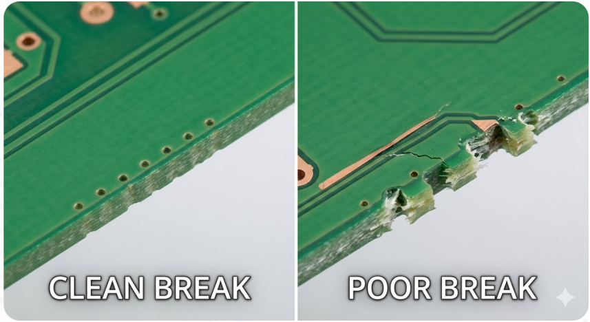
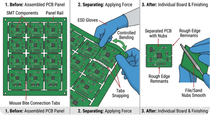
Ensuring Clean Breakaways Without Board Damage
Even with perfect drilling, the depanelization step itself introduces risk. The goal is a clean fracture along the perforation line with minimal residual material and zero damage to the board proper. Here is how to plan for it:
- Keep critical traces and components at least 1.5 mm from the nearest tab edge. This buffer protects against micro-cracks that can propagate from the fracture zone into the board laminate.
- Plan your post-break edge cleanup strategy. A light pass with fine-grit sandpaper (220 grit) removes the remaining nubs without damaging the solder mask.
- Validate your depanelization method during the prototype run. For 3+ tabs, flush-cut pliers or a depanelization fixture give more controlled results than hand snapping.
- Never twist the board to separate it. Always apply a bending force perpendicular to the tab line. Twisting introduces torsional stress that can crack solder joints several millimeters away from the tab.
For the CH32V003 board, hand separation with flush-cut pliers works well given its small size and 2 to 3 tab configuration. Grip the panel frame, support the board from below, and apply steady downward pressure. The board should release with a clean snap.
Common Issues and Professional Solutions
Preventing Burrs, Cracks, and Incomplete Breaks
Three problems account for the vast majority of mouse bite failures in production. Let's address each one directly.
Burrs: The annoying fibrous bits of roughness that remain stuck to the cut. They become visible when the holes used in the perforation are too wide, and thus, thick FR4 bridges tear up rather than cut easily. The fix? Reduce the hole pitch to around 0.7-0.75mm and use flush-cut pliers as opposed to simply using your fingers.
Cracks: Fracture lines extending beyond the tab into the board, potentially damaging traces or solder joints. Usually caused by tabs that are too close to copper or too few tabs, forcing excessive breakout force. Increase the copper keepout to at least 0.5 mm and consider adding an extra tab to distribute force.
Incomplete breaks: The tab does not fully separate, requiring excessive force. This happens when the web of material between holes is too strong. Increase the number of holes, decrease the pitch, or widen the drill diameter from 0.5 mm to 0.55 mm.
Balancing Strength and Ease of Separation
Here is the fundamental tension in mouse bite design: the panel must be strong enough to survive automated assembly handling conveyors, pick-and-place vacuum nozzles, and reflow oven vibration. But they are weak enough that a human or simple tool can separate the boards without damage afterward.
If tabs are too weak, boards can break free during assembly -- a loose board inside a reflow oven jams conveyors and halts the production line. If tabs are too strong, the depanelization step flexes the board, stresses solder joints, and risks delamination near the break zone.
The following table summarizes the tradeoffs:
| Parameter | Too Weak | Too Strong |
| Symptom | The board detaches during reflow or handling | Requires excessive force to separate |
| Root Cause | Too many holes, too large drill, too narrow tab | Too few holes, too wide pitch, too wide tab |
| Fix | Reduce holes by 1-2, increase tab width by 0.5 mm | Add 1-2 holes, decrease pitch by 0.05-0.1 mm |
JLCPCB's Expertise in Mouse Bite Fabrication
Advanced Panelization and Depanelization Capabilities
When you upload a panelized design to JLCPCB, their system recognizes panel structures and provides feedback on tab placement, mouse bite geometry, and rail dimensions. Their guidelines recommend perforation patterns validated across millions of panels, so you are building on proven manufacturing data.
A practical tip: communicate your panel intent early. For the CH32V003 board, a clear note like "no tabs on USB edge or programming header edge" saves a review cycle and prevents misplaced breakaway tabs. JLCPCB also supports mixed methods on a single panel, V-score on straight edges and mouse bites on irregular sections.
High-Yield Production with Consistent Quality
JLCPCB's standardized panel rules for consistent drill diameters, calibrated pitch spacing, and controlled routing depths. Tab geometry on panel number 1,000 matches panel number 1. This eliminates operator-dependent break variation and translates directly to yield.
Whether you are building 100 or 10,000 CH32V003 boards, the break quality stays uniform from first panel to last. When every tab breaks with the same force and leaves the same minimal residue, your depanelization step becomes predictable and fast.
Full Support from Design Review to Final Delivery
JLCPCB's engineering team also evaluates your panel layout during pre-production review, flagging tabs too close to components, weak perforation patterns, or rail dimensions too narrow for conveyor transport.
For your CH32V003 board, once a panel layout passes review and produces clean results in a pilot run, you have a reusable panel template. Future board revisions can reuse the same configuration without re-qualifying the mouse bite geometry, saving time and cost on every subsequent order.
Frequently Asked Questions (FAQ)
Q: Mouse bites vs V-score: when should each be used? 1
Use V-scoring when your board has straight edges on all sides and no components within 1 mm of the perimeter. Choose mouse bites for irregular outlines, internal cutouts, or connectors near edges. Many designs benefit from a hybrid approach: V-score on straight edges, mouse bites on complex ones.
Q: How many tabs should a small MCU board have in a production panel?
For a board in the 30 to 50 mm range like the CH32V003 (34.976 mm x 17.998 mm), two to three tabs are ideal. Two tabs are sufficient for single-sided reflow; add a third tab if the board goes through double-sided assembly or if it will be handled extensively before depanelization. More than three tabs on a board this size makes hand separation unnecessarily difficult.
Q: How do I avoid edge chipping near USB or connector-heavy regions?
Keep tabs away from connector edges entirely. If a tab must be placed near a connector, increase the keepout to at least 2 mm and reduce the number of holes by one or two. After depanelization, a light sanding pass cleans up any remaining nub without risk to nearby solder joints.
Q: Q. Can I use the same mou1se bite geometry for prototype and volume builds?
Yes, and you should. Once you validate a perforation pattern (say, 5 holes at 0.5 mm diameter with 0.75 mm pitch on a 3 mm tab) during your prototype run, use exactly that geometry for production. This eliminates one more variable from your pilot-to-volume transition.

Keep Learning
How to Design and Manufacture Reliable Slot Holes in PCBs
Key Takeaways Slot holes are elongated openings ideal for flat pins, connectors, shields, and board alignment. Minimum sizes: 0.5 mm (plated) and 1.0 mm (non-plated); prefer rounded ends with length ≥ 2.5× width. Maintain proper annular ring, edge clearance, and DFM rules to prevent breakout and plating issues. Use overlapping drills for short plated slots and routing for longer ones. Good slot design greatly improves mechanical strength, thermal performance, and assembly reliability. JLCPCB’s precisi......
How Beveled Edges Improve Reliability and Performance in Card Edge Connectors
Key Takeaways Beveled edges enable smooth insertion and protect gold fingers from wear in card edge connectors. Use 30° or 45° angles (45° is standard for most designs) with depth of 1/3 to 1/2 board thickness. They reduce insertion force, prevent plating damage, and improve long-term contact reliability. Proper beveling is critical for high-cycle applications like DDR modules and PCIe cards. Bevel edges came into my attention the first time a memory module that I designed scratched its own gold finge......
How to Prepare Perfect Gerber Files for Flawless PCB Production
Key Takeaways Use RS-274X format and consistent millimeter units for all files. Always include complete layers: Copper, Solder Mask, Silkscreen, Board Outline, and NC Drill. Check your Gerbers in a viewer before uploading to catch errors early. Follow DFM rules: proper annular rings, solder mask expansion, and trace spacing. Use clear file naming and detailed fabrication notes. After spending weeks working on the perfect board layout, the routing is clean, the DRC passes, and you hit “export.” Two day......
Technical Guidance: V-Cut Panelization Standards
For boards with regular rectangular shapes, V-cut (V-scoring) panelization is an efficient method. This process involves cutting V-shaped grooves of a specific depth on both sides of the panel along the board boundaries, leaving a thin web of material (typically about 1/3 of the board thickness) that allows easy manual separation after SMT assembly. After separation, minor thread-like fibers or rough edges may remain and can be lightly scraped off. Due to material expansion and cracking during depanel......
Technical Guidance: Character Design Specifications
To facilitate component assembly, future maintenance, and traceability of PCB manufacturing information (such as manufacturer, production date, batch number, etc.), various character markings are typically silk-screened onto the PCB. These include component designators, polarity marks, test point labels, company logos, and production traceability information. Traditional PCB character silk-screening uses the screen printing process, hence the term “silk-screen characters.” High-definition characters a......
Technical Guidance: Mouse Bite Panelization Guide
The conventional method of panelization uses V-grooves. However, for irregularly-shaped boards or special requirements (such as JLCPCB's economic SMT assembly), mouse bite panelization, which resembles postage stamps on an envelope, is required. PCBs panelized using this method are called "mouse bite panels" or "mouse bite connections". Mouse bite panelization can be referred to as "universal panelization." As long as there is a position to add mouse bites, boards of various shapes can be interconnect......