Maximizing Circuit Reliability with PCB Test Points and Smart DFT
17 min
- Introduction to PCB Test Points in Hardware Design
- Primary Types of Test Points and Physical Forms
- Best Practices on How to Use Test Points in Layout
- Integrating Test Points into Factory Automated Inspection
- JLCPCB's Advanced Precision Fabrication & Automated Testing
- FAQs about PCB Test Points
- Conclusion
Key Takeaways
- Early Fault Catching: Test points drastically reduce diagnosis time and prevent costly field failures.
- Standard Pad Sizing: Use 1.0 mm flat copper pads with 2.54 mm spacing for optimal fixture contact.
- Protect High-Speed Signals: Keep branch traces short to prevent capacitive loading and resonance.
- Single-Sided Access: Place all test pads on the bottom layer to cut fixture costs.
- Right Test for Volume: Use flying probe for prototypes and bed-of-nails ICT for mass production.
A PCB test point is the cheapest insurance you will ever buy for a board. It costs you a 1-mm (40-mil) circle of exposed copper. Leave it out, and the first fault can turn into a manual search with a needle probe, where one small slip may short two adjacent pins. A camera can inspect whether a solder joint looks correct, but only a probe can confirm that a net is electrically connected and carrying current as expected.
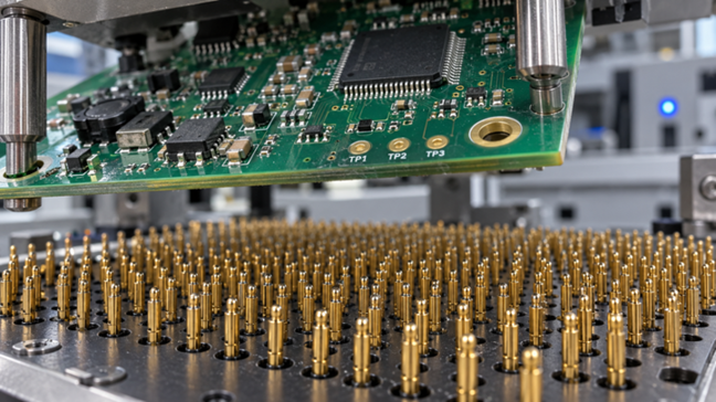
Figure 1: A bed-of-nails in-circuit test fixture closing onto a populated PCB
If a net has no accessible copper, pad, or test point, the tester cannot reach it. Test coverage is therefore something you draw during layout, not something you buy at the end. This guide covers what test points are and the three physical forms they take. It also covers the pad sizes and in-circuit fixture demands, why a fast net turns a test point into a stub, and what JLCPCB's own electrical test actually checks.
Introduction to PCB Test Points in Hardware Design
Two ideas sit behind this whole subject, and they get mixed up constantly:
- Test point: A physical copper feature that gives a probe access to a circuit net.
- Design for testability (DFT): The design process that determines which nets need test access and where those test points should be placed.
What are PCB Test Points and Why Do Engineers Need Them?
A PCB test point is a piece of conductive metal on a net, deliberately left uncovered by the solder mask so a probe can touch it. Its only job is to give a meter, an oscilloscope, or a factory tester electrical access to a node that would otherwise be sealed under mask. Engineers need them because a finished board hides nearly everything.
Solder mask covers most traces, while many important nodes sit under QFNs or between rows of BGA balls. Scraping away the mask to reach a trace is destructive, and the resulting probe contact is difficult to reproduce consistently. A tester can only check and isolate faults on nets it can physically access. If only 60% of the board’s nets have probe access, the remaining 40% sit outside the test program. Faults on those nets are not eliminated; they are simply more likely to escape factory testing and appear later in the field.
The Strategic Importance of Design for Testability (DFT)
Design for testability means adding features to a layout purely so the board can be tested later. It belongs in the same review as design for manufacturing, because both ask one question: can the factory physically do what your Gerber files imply?
- Bare-board test: A defect may cost only a few cents to scrap.
- Assembly test: The same defect can cost dollars to diagnose and repair.
- Field failure: It may mean a product return, repair work, and an unhappy customer.
Each step that pushes defect detection later can increase the cost by roughly 10×. Adding a test pad during routing costs nothing, since the copper is already on the net and a solder mask opening is not billed separately. Adding one after fabrication costs you a full respin. That is why testability belongs in your PCB design rules and best practices rather than in a review at the end.
Primary Types of Test Points and Physical Forms
Test points come in three physical forms, and the right choice depends entirely on who does the probing.
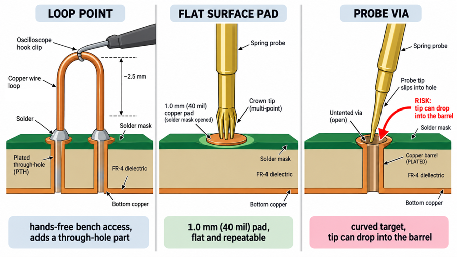
Figure 2: The three test point forms compared in cross-section
Loop Points vs. Flat Surface Pads vs. Probe Vias
- A loop point is a wire loop standing above the board surface, either a purpose-made through-hole part or a bent staple soldered into two holes. Its value is mechanical, because a scope hook or a crocodile clip can grip it hands-free. That makes it the right answer for bringing up on your own bench, where you need a probe to stay put while you type.
- A flat surface pad is a plain circle of bare copper with a solder mask opening over it. It adds no height, no part number, and no assembly step, so it is the default form for anything a machine will touch. Almost every test point in volume production is one of these.
- A probe via is an ordinary via with its mask tenting removed so a probe can land on the barrel. It is tempting because it costs nothing extra, but the surface it presents is a plated ring around a hole rather than a flat disc. A probe tip that lands off-center slides into the hole, which can give an intermittent reading and bend the pin.
| Test Point Form | What It Actually Is | Choose It When | The Trade-Off You Accept |
|---|---|---|---|
| Loop point | Wire loop standing 2 to 3 mm (80 to 120 mil) above the board | You need hands-free scope or clip access during bring-up | Adds a through-hole part, height, and an assembly step |
| Flat surface pad | Bare copper circle, 0.9 to 1.5 mm (35 to 60 mil), mask opened | A flying probe or an ICT fixture will touch it in the factory | Consumes the routing area on the probed side of the board |
| Probe via | Existing via with tenting removed, barrel exposed | Nothing else fits, and the net is low speed and non-critical | Curved target, tip can slip into the hole, poor repeatability |
| Component lead or pad | An existing exposed joint is used as the probe target | The board area is gone, and the joint is large and accessible | Probe force can crack a fillet or disturb a fine-pitch lead |
Key Characteristics of Test Point Pads and Vias
Size and spacing are not styling choices because they are set by the mechanical tolerance stack of the fixture. A spring probe is positioned by a drilled plate, and the board itself shifts by roughly 0.05 mm (2 mil) against its tooling holes. Your pad has to be big enough to absorb that whole stack.
| Test Pad Parameter | Absolute Minimum | Recommended Production Value | What Happens In Between |
|---|---|---|---|
| Pad diameter, signal net | 0.8 mm (31 mil) | 1.0 to 1.27 mm (40 to 50 mil) | Contact repeatability falls, so intermittent opens get reported |
| Pad diameter, power, or ground | 1.0 mm (40 mil) | 1.5 to 2.0 mm (60 to 80 mil) | High current probing needs an extra contact area |
| Probe centre-to-centre spacing | 1.27 mm (50 mil) | 2.54 mm (100 mil) | Below 100 mil, the fixture needs guided plates and costs more |
| Clearance to the component body | 0.5 mm (20 mil) | 1.0 mm (40 mil) | The probe barrel fouls the part instead of hitting the pad |
| Clearance to tall parts above 6.4 mm | 2.0 mm (80 mil) | 5.0 mm (200 mil) | The fixture plate cannot close flat over the component |
| Clearance to the board edge | 3.2 mm (125 mil) | 3.8 mm (150 mil) | Edge support rails and the router bite into the probe zone |
| Via barrel used as a probe target | 0.36 mm (14 mil) hole or smaller | Use a dedicated pad instead | A larger barrel swallows the tip, and the reading goes intermittent |
Probe spacing drives fixture cost harder than pad size does. Anything you hold at a 2.54 mm (100 mil) grid uses standard hardware. Anything tighter needs a guided plate, which adds weeks and money.
A spear tip concentrates force into a point, so it punches through flux residue and oxide. A crown tip spreads the load across a ring of sharp edges, which suits clean plated pads. Typical spring force runs 100 to 200 grams per probe, and that number adds up fast on a dense board.
Best Practices on How to Use Test Points in Layout
Placement rules exist to keep a mechanical fixture working, so they read as clearances rather than as electrical rules.
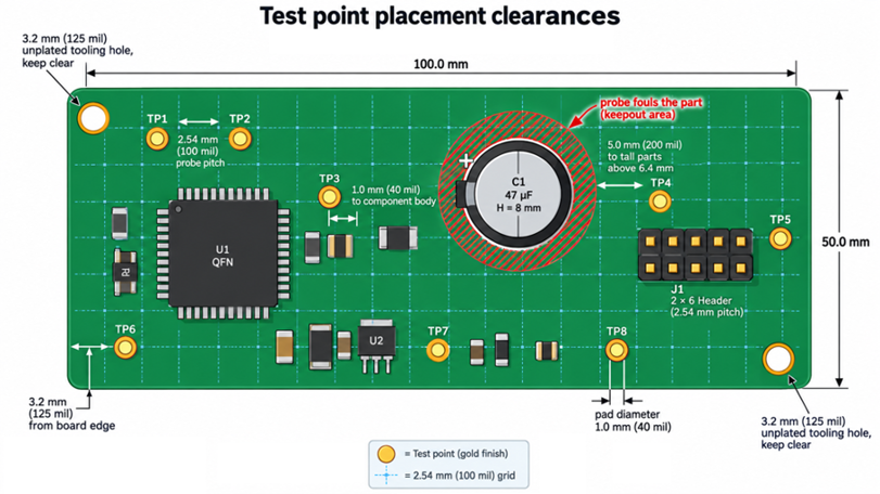
Figure 3: Test point placement clearances on a populated board
Rules for Placement, Clearance, and Grid Spacing
- Keep test points on one side: Place all probe targets on one side of the PCB, preferably the bottom. Double-sided fixtures need two probe plates and a clamshell mechanism, increasing cost and build complexity.
- Provide tooling holes: ICT fixtures align the PCB mechanically. Add at least two 3.2 mm (125 mil) unplated tooling holes in opposite corners, with adequate clearance from copper and components.
- Leave space for board supports: Each probe can apply roughly 100–200 g of force. A 500-probe fixture can therefore place 50–100 kg of total force on the PCB. Support pillars are needed to prevent board flex, so leave suitable, clear areas for them.
- Label test points clearly: Mark each point on the silkscreen with a designator such as TP1 or TP12. Keep the text beside the pad, not over it.
- Keep ink away from probe surfaces: Silkscreen inside the exposed test-pad area can contaminate the contact and cause falsely high resistance readings.
Optimizing High-Speed Signal Traces to Avoid Parasitic Capacitance
On high-speed nets, a test point is no longer electrically invisible. Its copper pad adds a small amount of capacitance, typically around 0.2–0.5 pF for a 1 mm pad over a nearby reference plane. That may be harmless on slower interfaces, but it can noticeably degrade very fast edges.
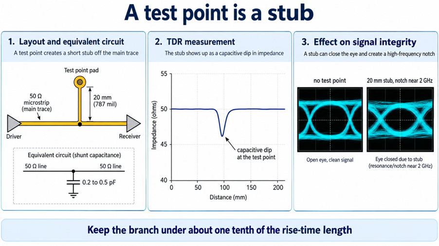
Figure 4: How a test point loads a high-speed trace
The larger problem is the trace branch leading to the pad. That branch acts as an open-ended stub and can create a resonance inside the signal bandwidth. On FR-4, even a 20 mm stub can produce a notch around 2 GHz. Keep the stub shorter than about one-tenth of the signal’s rise-time length. A 500 ps edge may tolerate roughly 8 mm, while a 100 ps edge may allow less than 2 mm.
Best practices are simple:
- Place the test pad directly on the signal path where possible.
- Keep unavoidable branches extremely short.
- Move testing to the slower side of a buffer or redriver.
- On very fast links, omit test points and use boundary scan, such as IEEE 1149.1.
Teardrops do not solve this problem because they add copper. Via-in-pad removes via stubs, but not the capacitance of the test pad itself.
Integrating Test Points into Factory Automated Inspection
A test point only earns its copper if a machine in the factory uses it. Two machines do, and they operate on completely different economics, so knowing which one will run your board changes how you draw the layout.
Flying Probe Testing vs. In-Circuit Testing (ICT) Fixtures
A flying probe tester moves a small number of probes around the board on high-speed gantries and touches targets in sequence. Because the program is generated from your CAD data, there is no fixture to build, and design changes are handled by editing a file.
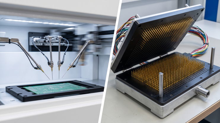
Figure 5: Flying probe testing compared with a bed-of-nails fixture
An in-circuit tester presses the whole board onto a custom bed of nails at once. It can drive hundreds of nets simultaneously, which is why it clears a board in seconds rather than minutes. That speed is bought with a fixture costing thousands of dollars. It takes weeks to build, and it becomes scrap the moment you move a test pad.
| Aspect | Flying Probe Test | In-Circuit Test (Bed of Nails) |
|---|---|---|
| Fixture needed | None, the program comes from CAD data | Custom drilled plate, thousands of dollars, and weeks of lead time |
| Time per board | Tens of seconds to several minutes | Typically under 30 seconds |
| Cost per board | High, since machine time dominates | Very low once the fixture is paid off |
| Response to a layout change | Edit the program and rerun | Rebuild or scrap the fixture |
| Best economic fit | Prototypes and runs up to a few hundred boards | Sustained production of thousands of boards |
| What it demands from you | Accessible copper anywhere on the net | Pads on a grid, one side, with tooling holes |
In-circuit test runs on an assembled board and measures the parts. It reads resistor values, checks capacitor ranges, confirms diode and electrolytic polarity, and finds shorts introduced by solder. The hardware looks similar because both can use flying probes or a nail bed. They answer different questions, so neither substitutes for the other.
Streamlining Manufacturing Workflows to Lower Defect Rates
Optical inspection and electrical test answer different halves of the same question, which is why a modern line runs both. A camera reports that a joint looks wrong, while a probe reports that net 47 is open between U3 pin 12 and R21. The second statement sends a technician straight to a location, so diagnosis time drops from minutes to seconds.
A well-instrumented assembly line runs its checks in a fixed order. Each stage catches defects while they are still cheap to fix, so nothing expensive travels far down the line.
- Bare-board electrical test verifies the net list before a single component is placed, so a fabrication fault never absorbs the cost of assembly.
- Solder paste inspection measures paste volume and offset right after printing, which is where a large share of downstream solder defects originate.
- Automated optical inspection after reflow catches missing parts, wrong polarity, tombstones, and visible bridges.
- X-ray inspection looks through BGA, QFN, and LGA bodies at joints that no camera can see.
- The flying probe or ICT then confirms electrically that the assembled nets behave, using the test points you provided.
- Functional test powers the board and exercises it against your product specification.
Test points also pay off after the board ships. A field engineer with a schematic and a labeled TP grid isolates a fault in minutes. An unlabelled board turns every repair into an exploration.
JLCPCB's Advanced Precision Fabrication & Automated Testing
Knowing what your manufacturer actually tests changes what you need to add yourself. It is worth checking that before you send the design to fabrication, because the gaps are the parts you have to cover.
Seamless DFT Support with Flying Probe and Bed-of-Nails Testing
JLCPCB's bare-board electrical test uses both technologies, with selection based on volume. Flying probes handle prototypes and small quantities, since there is no fixture to build for a five-board order. Large production runs move onto a bed-of-nails universal grid fixture because per-board time dominates cost at that scale.
On the assembly side, flying probe testing of a populated board is offered as an optional SMT service for prototypes and low-volume runs. Component-level in-circuit test with a custom bed of nails is not part of the standard PCBA flow. If your product needs it, plan for a dedicated test house or your own fixture.
A functional test is available, but it works from your instructions rather than from a generic script. The Functional Test (FCT) service asks you to provide product photos or DFM drawings, along with a written test procedure, with a demonstration video preferred.
Ultra-High Precision E-Test & Optical Inspection Capabilities
Bare-board electrical test comes in two grades at the quote stage, and the difference matters. The sampling test is free and carries a stated minimum pass rate of 99%. That means a portion of the boards in your order are tested rather than all of them. The full test checks every board and carries a fee, because probing every net on every board takes real machine time.
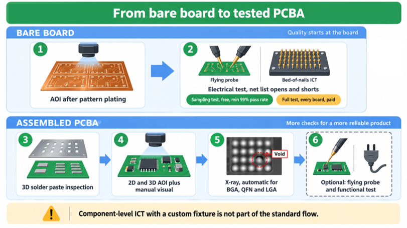
Figure 6: The JLCPCB test and inspection flow from bare board to assembled PCBA
Optical inspection runs alongside the electrical test throughout fabrication. Automated optical inspection after pattern plating photographs each panel and compares the etched copper against the design data. That catches nicks, slivers, and shorts in fine features before the board is drilled and finished. 3D solder paste inspection measures the print. 2D and 3D AOI are then performed to check placement and joints after reflow, and operators add a manual visual pass. X-ray inspection runs automatically when the system finds BGA, QFN, or LGA parts in your bill of materials, since a camera cannot see those joints.
FAQs about PCB Test Points
Q: How many test points does my board actually need?
For full in-circuit test coverage, the target is one probe site on every net. Each isolated power and ground rail wants two or more. Most prototypes stop far short of that and cover only the power rails, the reset and clock lines, and the debug interface, which is usually enough for bench work.
Q: Can I use an existing component pad instead of adding a test point?
You can, provided the joint is physically large and fully exposed, such as a 1206 resistor pad or a connector pin. Avoid it on fine-pitch or leadless packages. A probe force of 100 to 200 grams applied to a small fillet can crack the joint you were trying to verify.
Q: Do test points need to be on the bottom layer?
Not strictly, but putting them all on one side lets the fixture use a single probe plate instead of a clamshell. That roughly halves its cost and lead time. The bottom side is the usual choice because it normally carries fewer tall components.
Q: Will a test point ruin a USB or Ethernet signal?
Not on its own at those speeds. A 1 mm pad adds roughly 0.2 to 0.5 pF, which costs under 30 ps of rise time. The risk comes from the branch trace reaching the pad, so keep that branch under about 8 mm (315 mil) for a 500 ps edge.
Q: What is the difference between a test point and a test coupon?
A test point is exposed copper on your own board that lets a probe reach a specific net, and it stays there permanently. A test coupon is a separate sample strip in the panel border. It qualifies the fabrication process, such as impedance or plating thickness, and it is cut away during testing.
Conclusion
A PCB test point looks like an afterthought and behaves like an architectural decision. The copper is free while the layout is open. The coverage it buys decides whether a dead board takes ten minutes to diagnose or a week. That asymmetry is the whole argument for treating testability as a routing constraint rather than as a courtesy.
Three ideas carry across every board you will draw:
- Size test pads from fixture tolerances: Pad dimensions should follow the fixture’s tolerance stack, not personal preference.
- Place high-speed test points carefully: On fast nets, a test point adds capacitance and can behave like a stub.
- Understand what each test checks: Bare-board electrical testing verifies the copper. In-circuit testing verifies the assembled components and connections.
Plan the probe grid at the same moment you plan the stackup, and the test program writes itself later. JLCPCB's bare-board electrical testing, automatic X-ray of hidden packages, and optional flying-probe service cover most of what a prototype needs. That leaves your own effort free for the coverage only your design can provide.

Popular Articles
• The Comprehensive Guide to Circuit Symbols: Key to Understanding Electrical and Electronic Diagrams
• Design Guidelines for PCB Using FR4 Substrates
• Choosing the Best PCB Color-Enhancing Aesthetics and Functionality
• PCB Silkscreen: All You Need to Know
• PCB Board Design: A Step-by-Step Guide for Beginners
Keep Learning
Maximizing Circuit Reliability with PCB Test Points and Smart DFT
Key Takeaways Early Fault Catching: Test points drastically reduce diagnosis time and prevent costly field failures. Standard Pad Sizing: Use 1.0 mm flat copper pads with 2.54 mm spacing for optimal fixture contact. Protect High-Speed Signals: Keep branch traces short to prevent capacitive loading and resonance. Single-Sided Access: Place all test pads on the bottom layer to cut fixture costs. Right Test for Volume: Use flying probe for prototypes and bed-of-nails ICT for mass production. A PCB test p......
The Comprehensive Guide to Circuit Symbols: Key to Understanding Electrical and Electronic Diagrams
Note Need a quick reference while reading schematics? Download our free, printable Circuit Symbols Cheat Sheet (PDF), featuring the most common IEC and ANSI symbols organized by category. Keep it on your desktop or print it for easy reference at your workbench. ⬇ Download the Free Circuit Symbols Cheat Sheet (PDF) Every electronic diagram is written in a visual language, and circuit symbols are its alphabet. From your first electrical schematic to a multi-layer board, knowing circuit symbols can make ......
Design Guidelines for PCB Using FR4 Substrates
Material substrate concerns are necessary while designing electrical circuit boards. This is due to the fact that printed circuit boards cannot be manufactured without the appropriate PCB materials. When developing and producing circuit boards, the substrate material must be taken into account just as much as the copper layers, silkscreen, and surface polish. Generally speaking, non-conductive materials like porcelain, Marlon, FR4, and the like must be used for PCB substrates. Depending on its intende......
Choosing the Best PCB Color-Enhancing Aesthetics and Functionality
Key Takeaways Choosing the best PCB solder mask color involves balancing aesthetics, visibility, and functionality. Green remains the top choice for superior contrast and inspection, while black offers premium appeal, white excels in LED applications, and other colors like purple and red provide unique design options. The ideal color depends on your priorities in inspection ease, thermal performance, and brand image, with minimal impact on electrical performance when using proper silkscreen contrast. ......
4 Layer vs 6 Layer vs 8 Layer PCB: How to Choose the Right Stackup
Random selection of layers in electronics may lead to serious signal integrity issues. That's why we always design our stackup before designing the PCB. Stackup decides the type of PCB and how it gonna perform under high-frequency conditions. There are a lot of things that directly affect the stackup of the PCB, related to impedance matching, routing density, signal and power integrity, electromagnetic compatibility (EMC), and cost. Knowing the requirements before design and the most critical componen......
PCB Silkscreen: All You Need to Know
Key Takeaways The PCB Silkscreen Guide demonstrates that a properly designed legend layer is essential to prevent assembly failures and ensure long-term hardware reliability. By mastering modern manufacturing methodologies like Direct Legend Printing (DLP) and aligning layouts with JLCPCB's strict DFM design rules—including the absolute 0.8 mm character height limit and the automated 0.15 mm silkscreen clipping protocol driven by solder mask precedence—engineers can seamlessly eliminate cold joints an......