
Solder Mask on PCBs : Protecting Traces, Guiding Assembly, and Boosting Long-Term Reliability
9 min
- Defining Solder Mask and Its Core Functions
- Types and Material Options for Solder Mask
- Essential Design Rules for Effective Solder Mask
- Solder Mask Application in Professional Manufacturing
- Frequently Asked Questions (FAQ)
As we wear masks to save us from pollution, in the same way, the ones used by PCB to avoid contamination and oxidation. It became a very important step in PCB manufacturing over the years. In the early days, the manufacturers were more focused on one type of color, but today we have multicolor PCBs. That’s how the soldermask process evolved over the years. From protecting delicate copper traces to ensuring precise soldering during assembly. The solder masks directly influence yield and long-term field performance. In this article, we will develop our Understanding of what a solder mask is. How it is applied, and how solder mask design rules affect manufacturability.
Defining Solder Mask and Its Core Functions
What Exactly Is a Solder Mask Layer?
A solder mask is a thin, polymer-based insulating layer applied over the copper features. It is applied on the top surface of a PCB, leaving only component pads and specific areas uncovered. It acts as a protective coating and insulates copper traces.
When engineers ask what a solder mask is, the simplest answer is: It is the PCB’s first line of defense against solder shorts, corrosion, and accidental electrical contact. From a CAD perspective, the solder mask layer is generated as a negative image relative to copper pads. This image is transferred onto the board using photoimaging processes, ensuring precise alignment with copper features. We will discuss the full process in detail in the next sections.
Primary Roles in Trace Protection and Solder Control
The functional roles of solder masks can be divided into three critical domains:
1. Electrical Protection
Bare copper is vulnerable to oxidation and ionic contamination. Moreover, the tracks may cause accidental shorting. The solder mask electrically insulates traces, especially in dense layouts with fine pitch routing.
2. Solder Flow Control During Assembly
During reflow, the molten solder naturally wants to spread. Solder masks restrict solder wetting only to exposed pads, which prevents:
- Solder bridges between fine-pitch pins
- Tombstoning caused by uneven solder distribution
- Excess solder wicking along traces
3. Mechanical and Environmental Shielding
Soldering masks protect copper from humidity, flux residues, dust, and handling damage. In this way, exposing the circuit to the outside world does not harm the board material.
Historical Development and Modern Necessity
The initial PCBs did not have solder masks due to their manual soldering and very high pad separation. Nowadays due to surface-mount technology boards became more densely packed. The solder masks formerly available as optional coverings were now a mandatory step. The solder mask is utilized today to cover:
- Fine-pitch BGAs
- Microvias and HDI designs
- Automated optical inspection (AOI)
The absence of a well-designed solder mask would make reliable assembly nearly impossible. Modern electronics manufacturing depends on precise solder mask application to maintain consistency at scale.
Types and Material Options for Solder Mask
Liquid Photoimageable (LPI) vs Dry Film Masks
Liquid Photoimageable (LPI) solder mask is the industry standard for rigid PCBs. It is applied as a liquid coating and then photo-patterned using UV exposure. It is widely used in the electronics industry to fabricate high-resolution features. The process is quitematured and provides excellent adhesion to FR-4. It is very cost-effective for mass production and can be automated using machines.
Dry film solder masks are laminated sheets patterned similarly to photoresist. While they offer uniform thickness, they are less adaptable to uneven topographies. They are rarely used in modern high-density designs. But for most commercial and industrial boards, LPI remains the default choice due to its balance of precision and scalability.
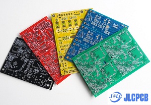
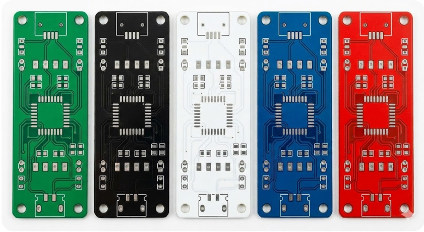
Standard Colors and Their Practical Implications
Green is the most common solder mask color. It is not just a cosmetic effect; the color selection also influences inspection and thermal behavior:
Green solder mask
- Best contrast for AOI systems
- Lowest cost
- Industry default
Black solder mask
- Preferred for consumer aesthetics
- Lower visual contrast for inspection
- Higher risk of hidden defects
White solder mask
- Used in LED boards for reflectivity
- Prone to discoloration from flux and heat
Blue and red solder masks
- Common in prototyping or branding
- Similar performance to green but higher cost
From a manufacturing standpoint, green remains the most inspection-friendly option.
Specialty Masks for Flexible or High-Temperature Boards
Flexible PCBs require solder masks that can withstand repeated bending without cracking. These are typically:
- Polyimide-based
- Thinner and more elastic than rigid board masks
High-temperature applications, such as automotive or aerospace electronics, demand solder masks with:
- Higher glass transition temperatures (Tg)
- Improved chemical resistance
- Stability during multiple reflow cycles
Choosing the wrong mask material can lead to delamination, cracking, or premature field failures.
Essential Design Rules for Effective Solder Mask
Clearance, Dam, and Web Requirements Around Pads
Solder mask design rules directly impact assembly yield. Key parameters include:
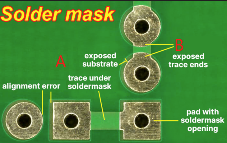
Solder mask clearance refers to the offset between the edge of a copper pad and the corresponding solder mask opening. Insufficient clearance can cause solder mask encroachment onto the pad and lead to poor solder wetting. On the other hand, excessive clearance may unnecessarily expose copper, which increasing the risk of oxidation.
A solder mask dam is the narrow strip of solder mask material left between adjacent pads. Its primary function is to inhibit solder bridging during reflow. Typical minimum dam widths fall in the range of 75–100 µm, though the exact value depends on the PCB manufacturer’s process capabilities.
Failure to adhere to these solder mask design rules can result in:
- Fragile mask slivers that peel off during fabrication or assembly
- Exposed copper areas that promote short circuits
- Compromised solder joints with reduced mechanical and long-term reliability
Avoiding Bridges and Ensuring Coverage Uniformity
To have a predictable solder behavior when assembling a product, it is necessary to avoid solder bridges and to have a uniform solder mask coverage. The variation in mask thickness or ill-defined holes may result in uneven wetting of the solder and a higher rate of defects, especially in fine pitch layouts. There are also problems with solder mask webs that are too thin to be consistently produced. The unwanted mask holes expose copper and allow solder wicking. To avoid such issues, designers must pay attention to solder mask layers when checking Gerber. Make sure their layouts fit within the capability of the fabricator early in the design process.
Integration with Vias, Traces, and Silkscreen Layers
Solder mask layer needs to be well incorporated with vias, traces, and silkscreen, also to make boards reliable. The vias can be tented, plugged, or left open with regard to their us,e but the copper traces should never be left exposed to oxidation and unintentional shorting. Silkscreen markings should not be located over solder mask openings that would interfere with soldering and testing. Appropriate coordination of these layers makes a great contribution to reducing rework, inspection failures, and assembly delays during production.
Solder Mask Application in Professional Manufacturing
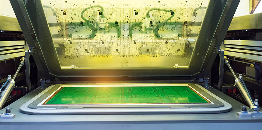
Coating, Exposure, and Development Processes
The solder mask application process typically follows these steps:
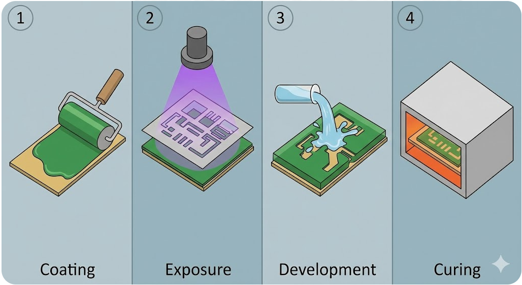
- Board surface cleaning
- Liquid mask coating (spray or curtain coat)
- Soft bake to remove solvents
- UV exposure through a phototool
- Development to remove unexposed areas
Precision at each stage is critical. Any misalignment or contamination can compromise solder mask integrity.
Curing Techniques and Thickness Control
After development, the board undergoes final curing, which is done using thermal and UV curing systems. Curing will ensure there will be enough chemical resistance and mechanical strength. Curing helps in better adhesion of the mask with the copper layers. Typical cured solder mask thickness ranges from 15–30 µm. Thickness outside this range can affect solder wetting and electrical insulation.
Quality Assurance for Adhesion and Durability
In professional PCB fabrication, the quality of the solder mask is not a matter of chance or fate. To ensure the mask remains in the right place, manufacturers subject the mask to a sequence of tests to ensure the mask does not float away during the reflow. Visual checks identify cracks and peeling that may expose copper. Adhesion tests ensure that the mask is well bonded and that it does not peel off after a few thermal cycles. Thermal shock testing makes sure that the mask can withstand the high and low temperatures quickly without breaking. The chemical resistance tests also confirm that the mask is resistant to the fluxes, and other environmental contaminants.
Advanced Benefits and Practical Considerations
Although the majority of designers believe that solder mask is just another method of controlling the process of solder flow, its advantages go far beyond assembly. An appropriately used solder mask greatly enhances the surface insulation resistance (SIR), which lowers leakage currents and prevents moisture and ionic contamination. It is also a protective shield against polluted, wet, or chemically hostile conditions and will make the board withstand the real world more than laboratory tests. This is one of the reasons why solder masks are not a negotiable item in industry, automotive, and outdoor electronics- the environment is not usually kind to bare copper.
Impact on Assembly Yield and Rework Efficiency

An effective solder mask design makes the manufacturing process very easy, quick, and less expensive. It increases the yield of a first-pass assembly process by placing the solder in its correct location, eliminates the manual work (no one loves to do it), and increases the accuracy of automated optical inspection by giving the object a distinct visual difference. All that translates to cheaper manufacturing expenses and hassle-free production processes. Bad solder mask design, however, is a traditional silent killer of evils. It is rarely directly pointed out as the cause of a problem, but often a root cause of long-term assembly errors, assembly rework, and late-night debugging.

Frequently Asked Questions (FAQ)
Q1. What is a solder mask, and why is it necessary?
A solder mask is a protective insulating layer that prevents solder shorts, protects copper, and ensures reliable assembly.
Q2. Are soldering masks electrically insulating?
Yes, soldering masks provide electrical insulation, but are not intended to replace conformal coatings.
Q3. Can solder mask design rules differ between manufacturers?
Absolutely. Always follow the specific design guidelines provided by your PCB fabricator.
Q4. Does solder mask color affect performance?
Electrically, no. However, color affects inspection accuracy, heat absorption, and the visibility of cleanliness.
Q5. Is solder mask optional for simple boards?
For prototypes, it may be optional, but for production, it is strongly recommended.
Keep Learning
Conformal Coating in PCB Technology: Benefits, Challenges, and Future Developments
If you're searching for conformal coating, you're likely looking for a reliable way to protect your PCB from moisture, dust, chemicals, or harsh environments. Choosing the right coating directly affects product reliability, performance, and lifespan. In this guide, you'll learn what conformal coating is, the main types available, and how to select the best option for your application. We'll also cover key benefits, application methods (manual, automated, and selective), as well as inspection, rework, ......
Preventing Black Pad Defects: Ensuring Reliable ENIG Finish in Professional PCB Manufacturing
Key Takeaways Black Pad is caused by excessive nickel corrosion during the ENIG immersion gold step, leading to brittle solder joints and hidden BGA/QFN failures. Key prevention methods: tight chemistry control (temperature, pH, time), consistent phosphorus content, and regular bath monitoring. High-reliability alternatives: ENEPIG (lowest risk) or nickel-free finishes like Immersion Silver and OSP. Always source ENIG from manufacturers with strict process controls. Ever get a great-looking board, wor......
Solder Mask Colors: Boost Your PCB Performance, Style & Reliability
Key Takeaways Solder mask color directly impacts AOI accuracy, thermal performance, and PCB reliability — it is not purely cosmetic. Green remains the industry benchmark for the highest manufacturing yields and fastest turnaround at no extra cost. White maximizes light reflection for LED applications, while black offers a premium aesthetic for high-end consumer products. Red and yellow provide superior visual contrast for prototyping, debugging, and safety-critical inspections. JLCPCB offers all seven......
Why Copper Oxidation Matters in PCB Design & How to Prevent It
Key Takeaways Copper oxidation is a critical concern in PCB design that directly impacts solderability, contact resistance, and long-term reliability. By understanding how oxidation forms and damages copper surfaces, designers can effectively prevent it through appropriate surface finishes (such as HASL, ENIG, and OSP), strategic solder mask application, and strict adherence to proper storage and handling practices per IPC-1601 guidelines. Protecting copper from oxidation ensures better assembly yield......
Comparing OSP Plating with Other PCB Surface Finishes
Key Takeaways OSP stands out as a cost-effective, ultra-flat, and environmentally friendly PCB surface finish with excellent solderability for fine-pitch components, making it ideal for high-volume consumer electronics. However, its short shelf life (3–6 months), sensitivity to handling and oxidation, and limited multi-reflow durability require careful storage and process control. When compared to HASL, ENIG, Immersion Silver, and Immersion Tin, OSP offers superior planarity and lower cost but trades ......
Hard Gold PCB Finish: Achieving Exceptional Wear Resistance and Contact Performance
Surface finishes are not all the same thing, and this is obvious beyond mention when you are dealing with parts that are beaten against one another over and over. Hard gold. The most common finish used when PCBs must complete hundreds or even thousands of insert-and-remove operations before going out of service is essentially a hard alloy of gold electroplated over a nickel barrier coating. The prototypical piece of evidence that demonstrates why this is important is the edge connector, otherwise know......