
PCB Silkscreen Explained : From Design Intent to Professional Application and Manufacturing Precision
8 min
- What Silkscreen Means in PCB Context
- Key Elements Included in Effective PCB Silkscreen
- Design Guidelines for Clear and Functional Silkscreen
- The Silkscreen Process in Professional PCB Manufacturing
- Common Silkscreen Challenges and Professional Solutions
- Frequently Asked Questions (FAQ)
Let’s come to the topmost layer of a PCB, which is about annotations. We all need some reference material to work on, and the same applies to the assembler, from component assembly to referencing different section legends and silkscreen plates; it plays an important role. In a finished printed circuit board, the silkscreen layer is the least technically appreciated element. It is the most helpful layer for the end user because we can not look into the layout, datasheets, and schematics. That’s how some simple boards have been designed over the years. In this article, we will understand the basics of a PCB silkscreen. We will see manufacturing limitations and professional application methods. Poor silkscreen design can slow assembly, cause polarity errors, and reduce serviceability.
What Silkscreen Means in PCB Context
Defining the Silkscreen Layer and Its Primary Purpose
Silkscreen PCB refers to the printed legend layer applied on the outer surfaces of a printed circuit board. You will find it typically on the component side (top) and sometimes on the solder side (bottom). This layer uses epoxy-based ink to print human-readable information directly onto the board. If asked what silkscreen is, the most accurate engineering definition is:
Silkscreen is a non-electrical PCB layer used to convey assembly, identification, and reference information for manufacturing, inspection, debugging, and servicing.
The silkscreen layer typically includes:
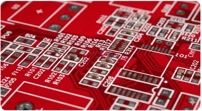
- Component reference designators (R1, C5, U3)
- Component outlines and orientation
- Polarity and pin-1 indicators
- Board name, revision, and date codes
Historical Role and Evolution in Modern Electronics
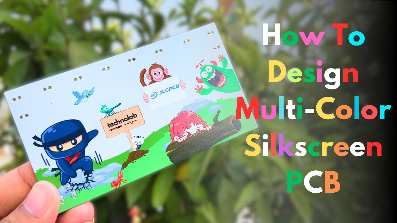
In early electronics, silkscreen was applied manually using stencil-based printing. Hence, the name silk screen is derived from there. As PCB density increased and automation became dominant, silkscreen evolved into a digitally imaged process. And see today, with JLCPCB, we have custom multicolor options:
Modern silk screen PCB processes now support:
- Fine text down to 4 mil line widths
- Automated optical inspection (AOI) compatibility
- High-contrast printing over the solder mask
- Long-term durability through multiple reflow cycles
Today, silkscreen is no longer optional. It is an expected deliverable in any professional PCB design.
Key Elements Included in Effective PCB Silkscreen
Component Outlines, Reference Designators, and Polarity Marks
One of the most critical functions of the PCB silkscreen layer is assembly clarity. A well-executed silkscreen acts as the silent guide for assemblers and future troubleshooters.
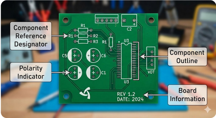
Reference designators ensure that every component on the board has a unique identity. They allow quick cross-checking against the BOM, speed up assembly verification, and are indispensable during debugging and repair. When a technician says, “Check R37,” we can look around on the PCB and troubleshoot around it.
Component outlines provide visual boundaries for each part. They indicate package size and correct placement, and reduce the risk of incorrect part substitution when multiple footprints look electrically compatible but are mechanically not.
Polarity and orientation markings are where silkscreen quietly prevents disasters. Clear indicators such as diode cathode bands, electrolytic capacitor polarity marks, IC pin-1 dots, or notches. The orientation arrows ensure components are placed correctly the first time.
Logos, Warnings, and Version Information
Silkscreen also communicates product-level metadata that becomes increasingly valuable over the board’s lifetime. This includes company logos and branding, board names or project identifiers, and hardware revision numbers. Here we can write information related to safety warnings, such as high-voltage or ESD sensitivity notices.
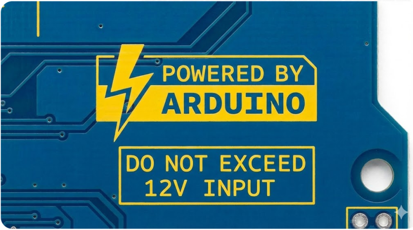
These markings prove invaluable during field servicing. A clearly marked revision number can save hours of confusion when multiple hardware versions are circulating. In short, a good silkscreen doesn’t just make a PCB readable.
Regulatory and Assembly Guidance Symbols
Many boards include standardized symbols such as:
- ESD warning icons
- Ground symbols
- Test point labels
- Programming headers identification
These elements improve communication between design and test teams.
Design Guidelines for Clear and Functional Silkscreen
H3: Font Size, Line Width, and Placement Rules
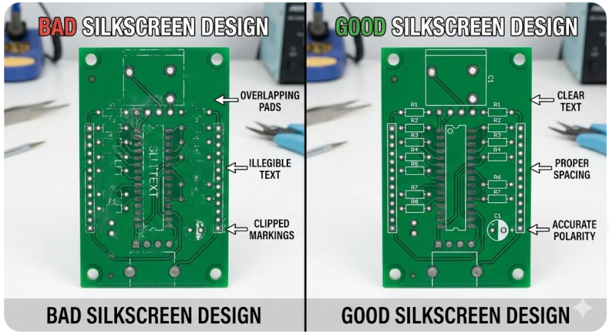
Understanding PCB silkscreen basics starts with respecting manufacturing constraints. Typical guidelines for better visibility are using a minimum text height of 30–40 mil with an absolute minimum text height of 25 mil. Preferably, the linewidth is ≥5 mil (better ≥6–8 mil). Text smaller than fabrication limits may disappear and become unreadable after reflow. Designers should prioritize clarity over density.
Avoiding Overlap with Pads, Vias, and Traces
One of the most common silkscreen errors is overlap with exposed copper features. Silkscreen ink must not be printed on solder pads and via holes. Because it may reduce the solderability during assembly, every fab follows a certain set of prioritization steps; always look into them before proceeding towards an order. If silkscreen overlaps pads, manufacturers will automatically clip or remove it. This often results in missing reference designators.
Color Choices and Readability Considerations
Silkscreen color is chosen for maximum contrast against the solder mask. High contrast improves assembly speed and AOI accuracy. Aesthetic choices should never compromise legibility. White silkscreen on green solder mask is the industry standard due to this. Some other preferable options could be White or yellow silkscreen on black solder mask and Black silkscreen on white solder mask.
The Silkscreen Process in Professional PCB Manufacturing
Ink Types, Curing Methods, and Layer Application
Modern PCB silkscreen services use epoxy-based inks applied through one of two methods. The more traditional method of transferring silkscreen ink onto printed circuit boards is conventional screen printing, which is a cheaper and more economical process. It is a process that involves pressing ink through a hard mesh stencil onto a board substrate. Although it is appropriate in low-density layouts where fineness is secondary, the technique gives relatively rough line weights, lower limit registration, and may lead to erosion or distortion of fine type and narrow component borders. Therefore, in simple boards or production applications where cost efficiency is the primary concern, standard screen printing can be used; however, this technique is not the best in high-component-density applications. After application, the ink undergoes:
- Thermal curing
- Or UV curing
DLI- Direct Legend Imaging (DLI) is a digital, non-contact silkscreen process that transfers the legend to the printed circuit board by exposing the legend to fine-controlled light. The method has high-resolution output, accurate registration, and better text fidelity, even of tiny reference designators and complex symbols. DLI has been preferred because of these properties in fine pitch components, dense populated assembly, and professional level designs, where legibility and positioning accuracy directly affect the yield in assembly and the reliability of inspection.
Integration with Solder Mask and Surface Finish Processes
In PCB manufacturing, the silkscreen layer is applied after the solder mask and surface finish processes, such as HASL, ENIG, or OSP. This sequencing is deliberate and critical. It prevents silkscreen ink from interfering with solderability. It will ensure strong adhesion to the solder-masked surface and maintain accurate alignment with exposed pads.
Equally important is material compatibility. The silkscreen ink must be suitable for the chosen surface finish. Otherwise, issues such as ink peeling or discoloration can appear over time, especially under thermal cycling or reflow conditions.
Quality Controls for Durability and Legibility
Manufacturers of professional PCBs impose tough quality standards on silkscreen. The inspections are concerned with legibility, alignment, integrity, and after-thermal stress testing adhesion. Even with a bad silkscreen, a board will still work electrically, but it will normally not be accepted as a professional or commercial board. The weak or inadequately clear markings are indicative of manufacturing danger. That is sufficient reason to flunk the board in severe production settings.
Common Silkscreen Challenges and Professional Solutions
Bleeding, Misalignment, and Fading Issues
Common silkscreen defects include:
- Ink bleeding on fine text
- Misalignment relative to pads
- Fading after reflow
- Partial text loss due to clipping

How Advanced Manufacturing Ensures Consistent Results
Modern fabs mitigate silkscreen risks through:
- Direct imaging instead of stencil printing
- Automated alignment systems
- Process capability enforcement
- Pre-production DFM checks
Following conservative PCB silkscreen basics during design ensures that what you draw is what gets printed.

Frequently Asked Questions (FAQ)
Q1. What is silkscreen in PCB used for?
Silkscreen provides assembly guidance, component identification, and product information.
Q2. Is silkscreen electrically functional?
No. It has no electrical role but strongly affects manufacturability and serviceability.
Q3. Can silkscreen be printed on solder pads?
No. It will be removed or clipped by the manufacturer to protect solderability.
Q4. Does silkscreen survive reflow soldering?
Yes, when properly cured using professional silkscreen inks.
Q5. Are PCB silkscreen services included by default?
Most professional PCB fabs include standard silkscreen services, though complexity may affect cost.
Keep Learning
Conformal Coating in PCB Technology: Benefits, Challenges, and Future Developments
If you're searching for conformal coating, you're likely looking for a reliable way to protect your PCB from moisture, dust, chemicals, or harsh environments. Choosing the right coating directly affects product reliability, performance, and lifespan. In this guide, you'll learn what conformal coating is, the main types available, and how to select the best option for your application. We'll also cover key benefits, application methods (manual, automated, and selective), as well as inspection, rework, ......
Preventing Black Pad Defects: Ensuring Reliable ENIG Finish in Professional PCB Manufacturing
Key Takeaways Black Pad is caused by excessive nickel corrosion during the ENIG immersion gold step, leading to brittle solder joints and hidden BGA/QFN failures. Key prevention methods: tight chemistry control (temperature, pH, time), consistent phosphorus content, and regular bath monitoring. High-reliability alternatives: ENEPIG (lowest risk) or nickel-free finishes like Immersion Silver and OSP. Always source ENIG from manufacturers with strict process controls. Ever get a great-looking board, wor......
Solder Mask Colors: Boost Your PCB Performance, Style & Reliability
Key Takeaways Solder mask color directly impacts AOI accuracy, thermal performance, and PCB reliability — it is not purely cosmetic. Green remains the industry benchmark for the highest manufacturing yields and fastest turnaround at no extra cost. White maximizes light reflection for LED applications, while black offers a premium aesthetic for high-end consumer products. Red and yellow provide superior visual contrast for prototyping, debugging, and safety-critical inspections. JLCPCB offers all seven......
Why Copper Oxidation Matters in PCB Design & How to Prevent It
Key Takeaways Copper oxidation is a critical concern in PCB design that directly impacts solderability, contact resistance, and long-term reliability. By understanding how oxidation forms and damages copper surfaces, designers can effectively prevent it through appropriate surface finishes (such as HASL, ENIG, and OSP), strategic solder mask application, and strict adherence to proper storage and handling practices per IPC-1601 guidelines. Protecting copper from oxidation ensures better assembly yield......
Comparing OSP Plating with Other PCB Surface Finishes
Key Takeaways OSP stands out as a cost-effective, ultra-flat, and environmentally friendly PCB surface finish with excellent solderability for fine-pitch components, making it ideal for high-volume consumer electronics. However, its short shelf life (3–6 months), sensitivity to handling and oxidation, and limited multi-reflow durability require careful storage and process control. When compared to HASL, ENIG, Immersion Silver, and Immersion Tin, OSP offers superior planarity and lower cost but trades ......
Hard Gold PCB Finish: Achieving Exceptional Wear Resistance and Contact Performance
Surface finishes are not all the same thing, and this is obvious beyond mention when you are dealing with parts that are beaten against one another over and over. Hard gold. The most common finish used when PCBs must complete hundreds or even thousands of insert-and-remove operations before going out of service is essentially a hard alloy of gold electroplated over a nickel barrier coating. The prototypical piece of evidence that demonstrates why this is important is the edge connector, otherwise know......