
Designing Durable Custom Keyboard PCBs: Tailored Solutions and Expert Fabrication
13 min
- Key Components in Keyboard PCB Builds
- Design Principles for High-Performance Keyboard PCBs
- Advanced Manufacturing Techniques for Keyboard PCBs
- Why JLCPCB is the Go-To Choice for Custom Keyboard Designers
- Frequently Asked Questions (FAQ)
So what's a keyboard PCB? In simple terms, it is the printed circuit board that is contained in the center of any keyboard, connecting the key switches to the controller, which communicates with your computer. Hitting a key closes a circuit on the PCB, which the controller records what key it was and transmits that keycode back to your host device. The mechanical-keyboard community is a subculture that has developed out of a niche hobby to become a successful subculture in the mechanical-keyboard world. It is the foundation that determines what a keyboard can do: what types of switches are supported, whether you can hot-swap components, how many LEDs you can be running at once, what layouts you can choose, and what features the board forfeits to the firmware.
A PCB transforms a stack of switches and keycaps into a smooth, fully customizable input pad. Mechanical-keyboard scene is fond of creating unique PCBs to flex inventive style. Depending on the tight 40% layouts to full-size boards with rotary encoders and OLED displays, the PCB design determines what you can literally build. And now that it is possible through cheap-price fab services to have custom boards produced at a price that hobbyists and indie designers can afford, the barrier to building your own keyboard is now lower than ever.
Evolution from Basic to Customizable Designs for Enthusiasts
In comparing the early keyboard PCBs, they were relatively simple; they were simply a grid of switch connections connected to a dedicated controller IC. Customization was mostly limited to some commercial choices that were only compatible with particular types of switches and fixed configurations. Today, the PCBs of custom keyboards have gone a very long way. The current boards have hot-swap sockets to replace switches without soldering, individually addressable RGB backlighting, and powerful ARM-based microcontrollers with open-source firmware such as QMK, VIA, or ZMK, which allows you to program key maps, macros, layers, tap-dance tricks, and more.
They are also USB-C, have optional Bluetooth, and can even support multiple physical layouts on a single PCB due to smart footprint design. This has been made possible due to the free and fully featured PCB design software such as KiCad, fabrication is cheap using a service like JLCPCB, and the open-source firmware ecosystem provides sufficient keyboard functionality without making you write your own custom software.
Key Components in Keyboard PCB Builds
Switches, Stabilizers, and Hot-Swap Sockets
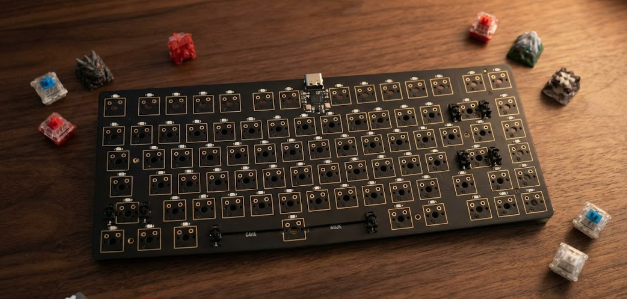
It is the switch that essentially is the star of any mechanical keyboard, and you must make sure that the PCB goes hand in hand with it. The switches we are mostly considering are MX compatible and have either a 2-pin or a 5-pin layout - the additional three pins assist in keeping the switch stable on the board. When you layout your keyboard PCB, you have to align those through-holes of the switch pins and mounting pins, and put the pads the right size so that you can solder them or, in the case of a hot-swap, the sockets remain firmly soldered in place.
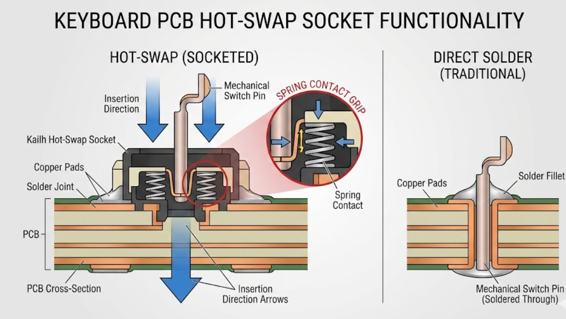
Hot-swaps (wonder Kailh or Gateron) are surface-mount components, which allow you to just drop in a switch without soldering. Due to that, the pad geometry alters slightly, and you also have to consider the mechanical aspect of it; the sockets need to endure a ton of insertions and remain down on the board.
It is the stabilizers that prevent the big keys from wobbling when you strike them without hitting the center. Holes or clip-in locations in your PCB have to be precisely where the plate-mount or PCB-mount stabilizers are. When they are out of commission, you will trigger one of the most irritating layout bugs: a wiggly space bar or a wiggly shift.
RGB LEDs, Controllers, and Interface Connectors
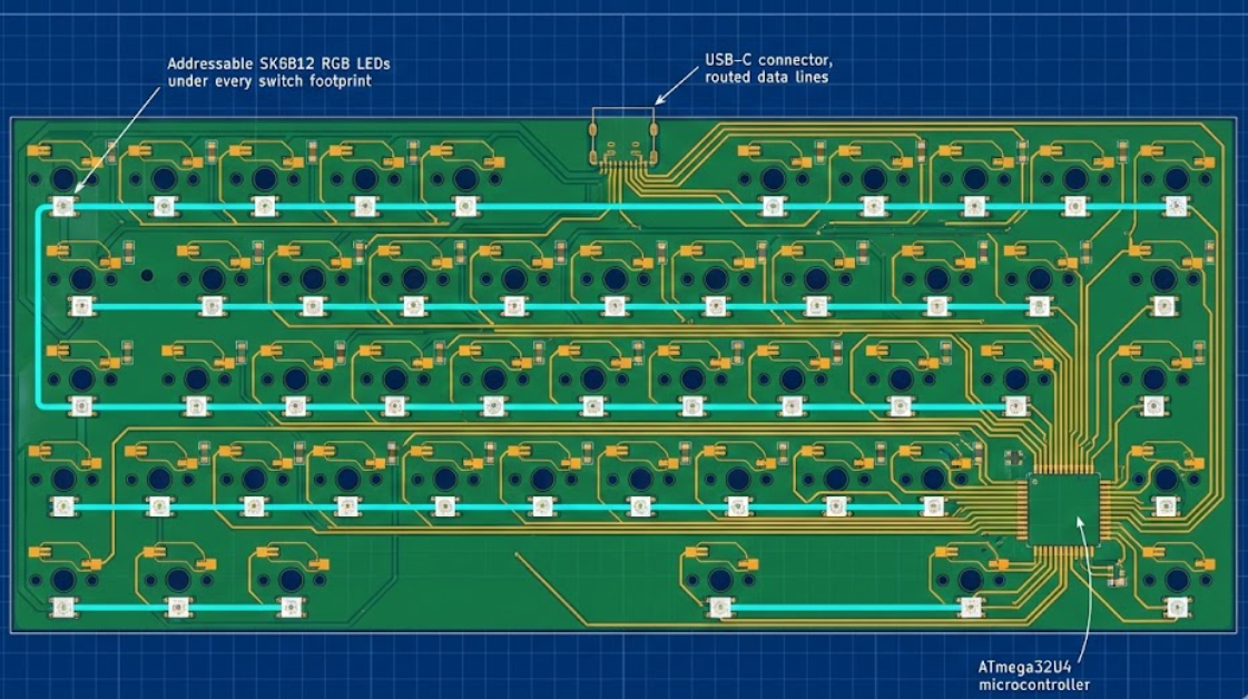
Per-key RGB lighting is expected by most people nowadays. Typically, that involves an addressable LED, such as SK6812MINI-E, and fitting it below the switch. They are daisy-linked, and therefore you must take care of that data line to ensure that the signal is strong throughout 60, 100, or more LEDs.
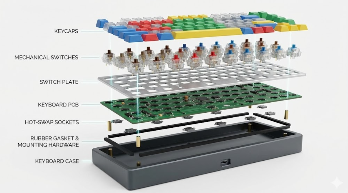
The controller is the brain of the keyboard. We generally use the ATmega32U4 due to the fact that it is the QMK base, but the STM32 is available in some cases where you wish to have additional processing power to do something fancy. The nRF52840 is one to consider in case you are going wireless, since it provides you with Bluetooth. All these chips come with varying pin numbers, package sizes, and peripheral requirements; thus, they actually define the way you lay the PCB.
USB-C is simply the new connector that is used in keyboards as of now- USB-C has substituted both Mini-USB and Micro-USB. USB-C footprint must be treated with a high degree of caution, particularly the CC pins, which indicate the direction in which the cable is inserted. In the case of wireless constructions, a JST connector to a LiPo battery and power-management circuit, typically a TP4056 charge controller, will also be added to the design.
Material Choices for Flexibility and Durability
Standard 1.6mm FR-4 is the most common substrate for keyboard PCBs; it is neither too stiff nor too expensive, and not too difficult to manufacture. When you are cutting a flex-cut design, going around an odd-shaped enclosure, you will discuss that you are going to use 0.8mm or even 0.6mm layers and open up the PCB in certain spots to create living hinges.
The color of the solder mask is important in this case, with many individuals opting to choose matte black in order to achieve a high-end appearance, some opting to use white, and some preferring the traditional green as a source of nostalgia. The last surface finish is typically HASL or ENIG; ENIG is the best to use in hot-swap assemblies since the exposed pads are visible and look neat.
Pro-Tip: If designing your first custom keyboard PCB, start with KiCad and the open-source keyboard PCB libraries available on GitHub. These libraries include pre-made footprints for MX switches, hot-swap sockets, stabilizers, and common controllers, saving hours of footprint creation.
Design Principles for High-Performance Keyboard PCBs
Layout Optimization for Key Mapping and Ergonomics
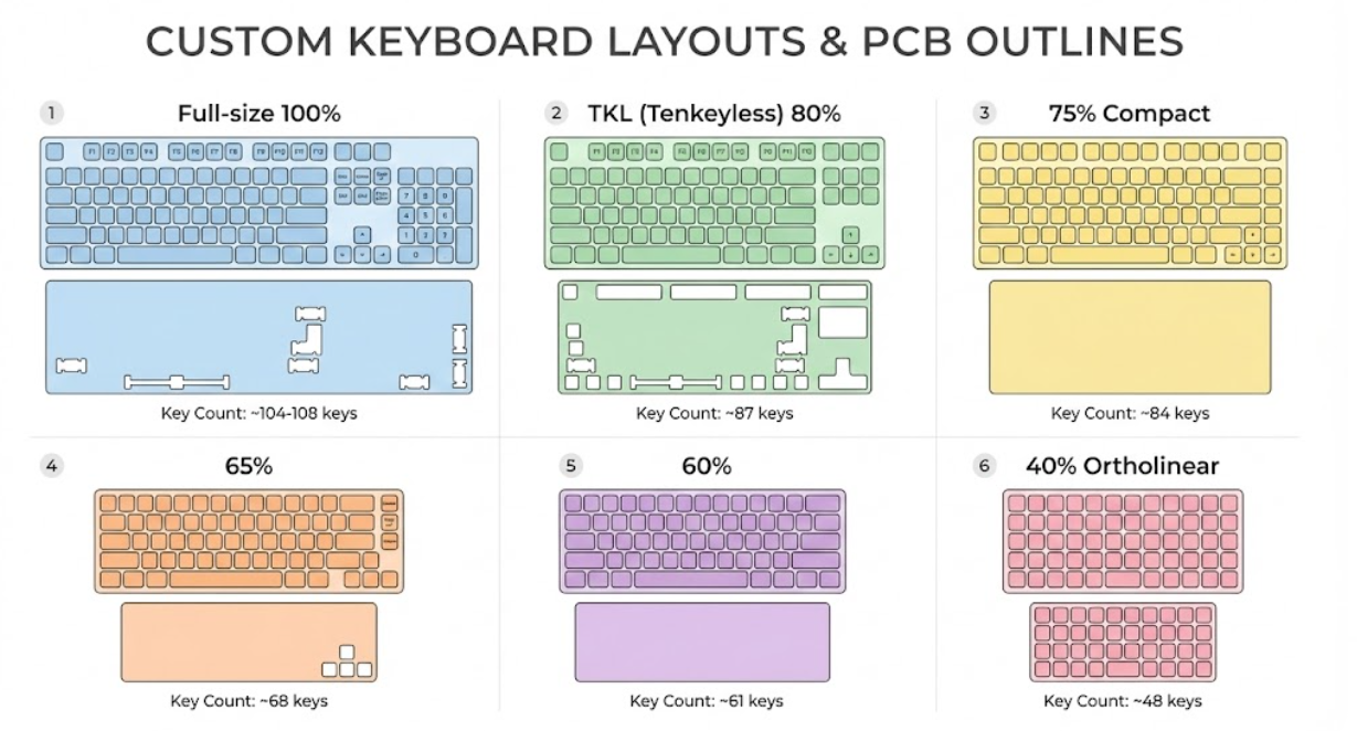
The design of keyboard layout begins by determining the way the actual keys are going to fit on the board. The standard ones, such as ANSI or ISO, are relatively pretty set, yet when you customize, such as ortholinear, split, Alice style, ergonomic, you have to plot out all the keycaps and the plate to make everything fit, so the keycaps and the plate are aligned. A common trick with a single PCB is to add footprints of all the layouts you want to support, even though some of these combinations are contradictory (such as having both split backspace and full-width backspace on the same board).
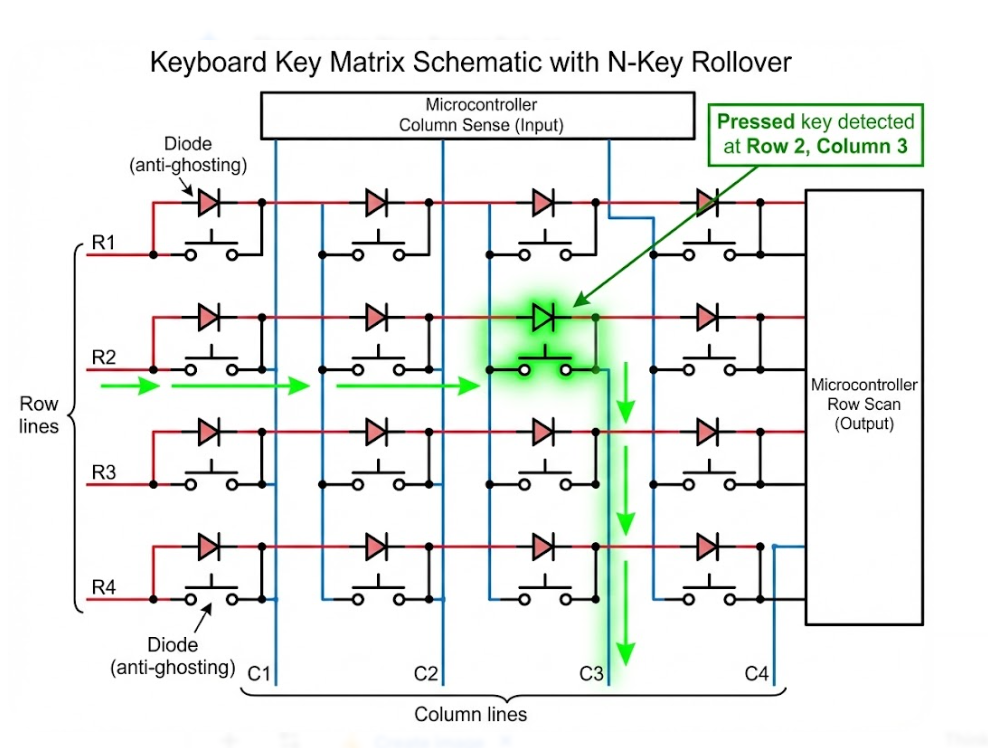
The firmware will create the electrical matrix such that the board functions in whatever setup you choose to create. The important matrix is simply switches laid out in rows and columns, and it informs you how many I/O pins the controller requires, as well as causing ghosting, the annoying false key taps when you press a bunch of keys concurrently. Ghosting is eliminated by adding a diode to each switch (which is now standard), and you now have complete N-key rollover.
Signal Routing and Power Distribution Strategies
It may seem simple to route the PCB with all these small traces, but it becomes a mess. In effect, you are laying out the matrix: every switch is connected to one line of row and one line of column by a diode. The greatest difficulty lies in maintaining those lines brief and concise. There is a bit of complexity provided by RGB LEDs. The data line is then bounced around each LED sequentially, and therefore, the longer the path, the poorer the signal.
Limit the traces to short and straight, stick a small 100 nF cap next to each power pin of the LEDs, and ensure the supply can take the maximum currents- up to 60 nA/LED as you power the brightness to maximum across a hundred LEDs. In the case of USB-powered keyboards, you must observe the 500mA limit (or 900mA on USB3.0). Full color at full brightness can readily cut that, and thus you require current limiting at the firmware level and traces of adequate size that do not sag voltage-wise.
DFM Rules to Enhance Manufacturability
In the case of manufacturing, tricks are few and far between. Use normal through-hole sizes of the switch pins (typically 1.5mm pad and 1.0mm hole of MX). Ensure that there is a clearance between the hot swap socket pad and the surrounding traces. Verify the USB-C footprint has the correct part number- other manufacturers have a slight variation in shape. And make all the LED footprints facing alike to make assembly painless.
Panelization is especially applicable to keyboard PCBs. The shape is long, so you can not just put it on a regular panel. Discuss with your fab what the best panel size is and add breakaway tabs where you are sure they will not interfere with the plate or the switches.
Advanced Manufacturing Techniques for Keyboard PCBs
Precision Layering, Etching, and Drilling Processes
In our PCB design project, we discovered that keyboard PCBs are typically two-layer, which makes fabrication straightforward, but requires high precision. The switch pins and mounting holes must be laid out precisely; otherwise, the switches will not fit into their places or will not fit the plate holes. A misalignment of 0.2mm can result in an annoying or impossible installation of a switch.
In more complicated designs with RGB LEDs, USB controllers, and wireless modules, we move up to four-layered boards. They provide dedicated power and ground planes, enhancing the distribution of LED power and reducing the EMI of the microcontroller. The additional layers also facilitate routing in the narrow sections around the controller.in congested areas around the controller.
Surface Finishes and Assembly Compatibility
The common type of surface finish depends on the way you are going to build the keyboard. HASL is the least costly and is suitable for hand-soldering projects, which is convenient when you are beginning your projects. ENIG provides a flatter surface, which is excellent in hot-swap sockets as it maintains better contact with the switch pins, and it appears nicer, in particular, in visible pad regions. When outsourcing the board to a professional reflow soldering provider, the two options will serve the purpose.
The compatibility of the assembly goes further to the choice of components. When placing an order for SMT assembly with JLCPCB, it is important to ensure that all the things you require, such as LEDs, diodes, resistors, capacitors, and hot-swap sockets, are present in their component library. The discovery of the unavailability of parts after the order is a typical source of delays that can put the entire project on hold.
Quality Testing for Switch Stability and LED Uniformity
In the case of testing the keyboards, we are concerned with the end-user experience. The electrical tests ensure that the matrix routes are all correct and that shorted or opened circuits do not exist. The hot-swap sockets are also tested by fitting switches in and out, to ensure that they can fit without the need to use excessive force. LED testing will make sure that all the RGB lights are functioning well; one dead or incorrectly colored LED is conspicuously visible and cannot be tolerated by users.
Dimensional inspection of the board establishes that the outline of the board, the positions of the mounting holes, and the positions of the USB connector are all as per the design of the intended case. In case of boards to be used in particular cases, a minor mistake in dimensions may not allow fitting and may lead to downstream assembly problems.
Why JLCPCB is the Go-To Choice for Custom Keyboard Designers
Custom Support for Hot-Swap and RGB Integrations
JLCPCB is now the fabrication shop for the custom keyboard market, and it is understandable. The accuracy of their service in the details of keyboard-PCB is impressive: they drill switch pins through-hole, assemble hot-swap connections and RGB LEDs with solid SMT parts, use a variety of colors of solder-mask in order to keep it looking fresh, and offer board thicknesses of ultra-thin flex to standard 1.6mm.
High-Precision Fabrication for Multi-Layer Builds
JLCPCB has the gamut of single-layer to multi-layer builds, simple 2-layer matrix, or complex 4-layer builds with wireless and RGB. They have controlled-impedance routing of USB, accuracy of PTH drilling switch footprints, and repeatable ENIG plating of hot-swap pads, which are all you need.
Reliable Delivery from Prototypes to Full Custom Runs
Hobbyists who make their own keyboards are everywhere, from a single, after-school project to a hundred or thousand group purchase. JLCPCB is accommodative of the entire spectrum, between five prototype boards to validate or five prototype boards to full-scale production to community buys. Their prices are fair, quality is solid, and turnaround is fast, making them the logical choice of keyboard designers at any level.
Frequently Asked Questions (FAQ)
Q. What is a keyboard PCB, and can I design my own?
A keyboard PCB is the circuit board that connects key switches to a controller, enabling your keyboard to function. Yes, you can absolutely design your own using free tools like KiCad, open-source keyboard libraries, and affordable fabrication from JLCPCB.
Q. Do I need hot-swap sockets, or should I solder switches directly?
Hot-swap sockets add cost and slightly increase board complexity but allow switch changes without soldering. For personal builds where you want to experiment with different switches, hot-swap is highly recommended.
Q. How many layers do I need for a keyboard PCB?
Two layers are sufficient for most keyboard designs, including those with basic backlighting. Four layers are beneficial for designs with extensive RGB backlighting, wireless modules, or complex controller circuitry, where dedicated power and ground planes improve performance and simplify routing.
Q. What firmware should I use for my custom keyboard?
QMK is the most popular open-source keyboard firmware, supporting an enormous range of controllers and features. VIA provides a GUI-based configuration layer on top of QMK. ZMK is the preferred firmware for wireless (Bluetooth) keyboard builds based on the nRF52840 controller.
Q. Can JLCPCB assemble my keyboard PCB with components?
Yes. JLCPCB offers SMT assembly services that can populate diodes, LEDs, resistors, capacitors, hot-swap sockets, and controller ICs. Provide your BOM and pick-and-place files with your order. Through-hole components like switches are typically installed by the end user after assembly.

Popular Articles
Keep Learning
How to Design a PCB with Flux.ai (Step-by-Step Guide)
Key Takeaways This step-by-step Flux PCB design tutorial demonstrates the complete workflow by creating a compact 15 × 15 mm USB 2.0 hub, refining the layout, routing high-speed differential traces, and preparing manufacturing files for JLCPCB PCB fabrication and assembly. We are all hearing news; new AI models are being released every month. And it has finally reached the schematic editor. Flux.ai is a browser-based AI PCB design tool with a built-in AI agent that behaves like a junior hardware engin......
How to Design Your Own Keyboard PCB: From Layout to Firmware
Designing a custom keyboard PCB is one of the most rewarding entry points into practical electronics. You not only get a really useful product on your desk, but also you learn schematic capture, matrix scanning, footprint selection, USB, and firmware. Most of the hardware engineers use the same skills that show up on professional boards. This guide walks the entire build from choosing switches, wiring the diode matrix, adding the microcontroller and USB-C, laying out the board, and flashing QMK or VIA......
Don't Let Design Errors Ruin Your Hardware: The Complete Guide to PCB Design Verification
Key Takeaways PCB design verification is the systematic process of validating layouts against electrical, signal integrity, and manufacturing rules before production, preventing costly board respins and launch delays. Schematic verification through Electrical Rules Check (ERC) catches floating inputs, power shorts, and footprint mismatches before layout begins. Design Rule Checking (DRC) ensures trace widths, clearances, and via sizes comply with your fabricator's manufacturing tolerances, especially ......
How to Determine the Right PCB Voltage Clearance for Safe and Reliable Designs
Key Takeaways Clearance is the air gap; Creepage is the surface path — both essential for high-voltage safety. Base spacing on peak voltage and follow IPC-2221 / IEC 60664-1 standards. Major factors: voltage, pollution degree, CTI, altitude, and conductor location. Use isolation slots, guard rings, and conformal coating to optimize spacing. Always run clearance calculations, DFM checks, and Hipot testing before production. Why do two copper traces that work fine at 5V suddenly arc over and burn at 400......
Mastering PCB Footprints: Design Best Practices for Reliable Manufacturing
Key Takeaways A PCB footprint (land pattern) translates component datasheet dimensions into copper pads, solder mask openings, paste apertures, silkscreen, and clearance areas that enable reliable soldering and assembly. Follow IPC-7351 standards and manufacturer DFM rules for pad dimensions, spacing, and layer design to minimize defects like solder bridging, tombstoning, and cracked joints. Choose between through-hole (THT) and surface mount (SMT) footprints based on electrical needs, thermal perform......
How Copper Thieving Balances Your PCB for Better Manufacturing Results
Key Takeaways Copper thieving adds non-functional copper patterns (dots, squares, or crosshatch) to balance copper density across PCB layers. This effectively reduces uneven plating (from 20-30% to <10%), board warpage, inconsistent etching, and impedance issues, delivering tighter tolerances, better solder mask adhesion, higher yields, and lower costs. For best results, target 40-60% copper density per layer, maintain proper clearances, and ensure stackup symmetry. When done right, it transforms comp......