Safeguarding Circuit Boards Against Breakdown Voltage Failure
14 min
- Fundamentals of Insulation in Electrical Circuits
- Key Factors Influencing Breakdown Voltage in Laminates
- Failure Mechanisms and Insulation Risk Mitigation
- JLCPCB's High-Voltage Laminates & Manufacturing Capabilities
- FAQs about Breakdown Voltage
- Conclusion
Key Takeaways
- Construction Matters: Breakdown voltage depends on stackup and defects, not raw material ratings.
- Stress Causes Failures: Heat and moisture degrade insulation over time, leading to field defects.
- Four Main Failure Modes: Insulation fails via internal voids, treeing, CAF growth, or surface tracking.
- Layout Design Fixes: Use dual prepregs, wider hole spacing, rounded trace corners, and isolation slots.
- Testing Split: Bare-board testing checks low-voltage net continuity, while hi-pot tests verify high-voltage safety.
Breakdown voltage is where a board stops insulating and starts conducting, and it is rarely where the datasheet said it would be. The board that fails in the field usually passes every test at the factory, so the schematic is not where the problem lives. Insulation does not fail like a fuse; it fails like a chip in a windscreen: a tiny flaw takes a small hit each cycle, and the damage spreads until, one day, the whole thing goes.
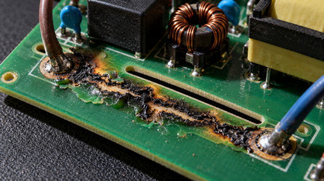
Figure 1: A carbonized breakdown track burned across the primary side of a mains PCB
Inside a laminate, that flaw is an air void, a glass bundle, or a film of dust on the surface. This guide covers what breakdown voltage really measures, how heat, moisture, and thickness affect it, and which four mechanisms kill a high-voltage board: partial discharge, treeing, filament growth, and surface tracking.
Fundamentals of Insulation in Electrical Circuits
Insulation is not a property you buy once and keep. It is a condition your board holds while heat, moisture, and voltage all work against it, so the useful question is how long it holds rather than how strong it starts.
What Is Breakdown Voltage and Why Does It Matter?
Breakdown voltage is the voltage at which a specific insulating structure stops blocking current and starts conducting. It belongs to an object rather than to a material, so it is quoted in kilovolts. Your 1.6 mm (63 mil) board has one, and the resin inside it does not.
Once the field pulls electrons free faster than the resin can trap them, the current avalanches. That discharge is hot enough to carbonize epoxy, leaving a permanent conductive channel behind. Insulation does not recover from breakdown, which is why the event counts as a failure rather than a fault. A barrier measured at 6 kV on the production line may hold only 3 kV after two years in a humid enclosure, because every stress it survives leaves damage behind. So, breakdown voltage is a starting value with a decay curve attached.
Distinguishing Breakdown Voltage from Dielectric Strengths
Dielectric strengths are material properties, measured in kV/mm on a thin laboratory sample. Breakdown voltage is what a built construction survives, measured in kV, so the two are not interchangeable. One describes the resin, while the other describes your stackup, the voids in it, and the copper edges inside it.
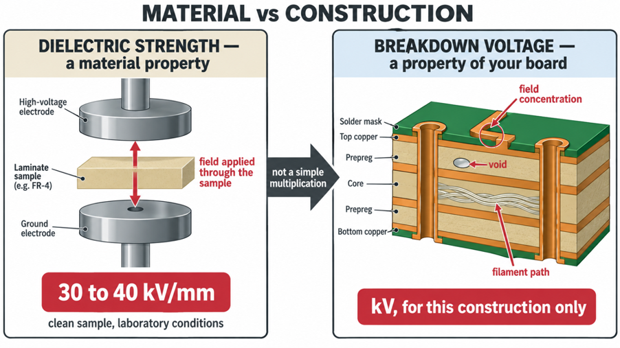
Figure 2: Material dielectric strength compared against the breakdown voltage
The two do not convert cleanly because breakdown never averages across a material. Current takes the weakest path it can find, so a single resin-starved patch decides the result for the whole ply. That is also why measured kV/mm falls as a test sample gets thicker. More material means more chances to hold a defect. Proving a barrier is a breakdown-voltage question, and only a test of the actual construction can answer it. That is because field solvers and datasheets both stop at exactly the point where manufacturing defects begin.
Key Factors Influencing Breakdown Voltage in Laminates
Three things move a laminate's breakdown voltage after the board is built, and none of them appear on a schematic. Heat, moisture, and the actual dielectric thickness between two traces all affect how the PCB behaves. So the value you qualify in the lab is not always the value the board sees in real-world operation.
Breakdown Voltage Influencing Factors: Temperature, Moisture, and Thickness
Temperature attacks the resin rather than the glass. Once the epoxy nears its glass transition temperature, it softens, and its bulk conductivity increases accordingly. Leakage current then further heats the resin, raising conductivity again. The practical guard band is to keep the continuous operating temperature 20-30 °C below Tg. A 130 °C Tg laminate operating at 110 °C has already used up most of its margin. So selecting the Tg of your PCB is a high-voltage decision, not only a reflow one.
Moisture does the same job more quietly. FR-4 absorbs only 0.1 to 0.2% of its weight in water, but that water collects along the glass interfaces where the field is strongest. Doubling a dielectric adds real withstand voltage while the kV/mm figure falls, because a thicker layer holds more glass bundles and more resin-starved spots.
| Stress in Service | What It Does to the Insulation | Effect Over Time | What Protects You |
|---|---|---|---|
| Operating temperature near Tg | Resin softens, conductivity rises, leakage self-heats | Falls steadily, can end in thermal runaway | Keep the continuous temperature 20 to 30 °C below Tg |
| Absorbed moisture | Water collects in resin and at glass interfaces | Up to 20% lower until the board is baked dry | Conformal coating, sealed enclosure, bake before testing |
| Thin pressed prepreg | Real gap is 0.1 mm (4 mil), not the 1.6 mm (63 mil) board | Sets the true inner-layer limit from day one | Two prepreg plies across a high-voltage boundary |
| Surface contamination | Dust and flux residue hold a conductive film | Surface path fails long before the bulk does | Clean and coat, and design creepage without the mask |
| Voids in the laminate | Air pockets ignite partial discharge under AC | Erosion from inside for months before failure | Low-void lamination, no single thin ply at the barrier |
Electrical Behavior of Common PCB Dielectric Materials
PCB dielectric materials differ less in raw breakdown strength than in how they age. Standard FR-4 is woven glass in an epoxy matrix, which gives it two weaknesses at once. The resin can carbonize, and the glass bundles give filaments a path to grow along. Stock FR-4 is a material group IIIa laminate, with a comparative tracking index between 175 and 400 V. If you need group II or group I for your safety file, request a high-CTI grade. Confirm availability before you commit to the layout.
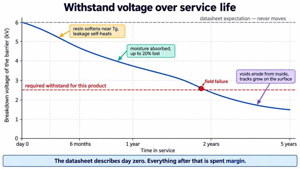
Figure 3: How heat, moisture, and time move a laminate's withstand voltage
| Laminate | Published Figures | How It Ages Under Voltage | Where It Earns Its Place |
|---|---|---|---|
| Nan Ya NP-140F, NP-155F | Tg 140 to 155 °C, standard FR-4 chemistry | Surface carbonizes first, glass bundles carry filaments | General mains-connected boards up to roughly 250 V working |
| Kingboard KB-6165F | Tg 150 °C, 65 kV parallel breakdown, CTI above 175 V | Group IIIa tracking, so creepage sets the real limit | The grade to name in the fab notes for documented mains work |
| Shengyi S1000-2M | Tg 170 °C, high-Tg FR-4 | Holds insulation resistance at 110 °C and above | Hot enclosures, thick multilayers, long thermal life |
| Aluminum IMS, HY-7000 | Dielectric layer withstands nearly 3 kV | Dielectric is buried, so tracking is not the failure path | LED drivers and power stages where heat dominates |
| Rogers RO4350B, PTFE | Low loss, stable Dk, tight thickness control | Very little dielectric heating, so no runaway loop | RF work and above roughly 1 kV, where loss heating matters |
Failure Mechanisms and Insulation Risk Mitigation
Breakdown reaches a board by four routes, and only one of them is fast. Partial discharge, treeing, and filament growth all work inside the laminate over months, while surface tracking and arcing work across the outside.
Inner-Layer Dielectric Breakdown vs. Surface Electrical Arcing
Inner-layer breakdown almost always starts in a void. A gas pocket has a relative permittivity near 1, while the epoxy around it has a relative permittivity near 4.4. The field inside that pocket is therefore about 4.4 times the field in the bulk resin. Air ionizes at roughly 3 kV/mm, so the void discharges long before the epoxy does.
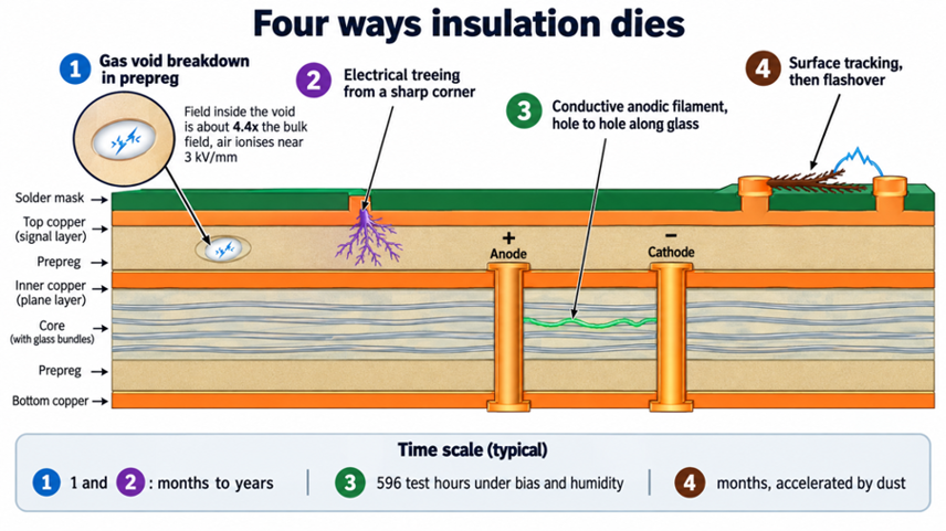
Figure 4: Partial discharge in a void, a growing tree, filament growth along glass
A 0.1 mm (4 mil) prepreg ply holding 400 V carries a field of 4 kV/mm. The void inside it sees 4.4 times that, which puts about 880 V across 50 µm of air, so discharge starts and then repeats on every mains cycle.
- Partial discharge: Each discharge is tiny, but repeated events slowly erode the polymer around a void. The damage can build up for months before the insulation finally breaks down.
- Treeing: Discharges follow strong electric-field paths through the resin, creating branching channels between conductors. Sharp copper edges and burrs can become starting points, making this both a material and a layout issue.
- CAF growth: Conductive anodic filament (CAF) growth does not need a discharge. Heat, humidity, and electrical bias can cause copper ions to migrate through glass fibers or glass-resin interfaces, eventually creating an internal short between holes.
| Mechanism | Where It Runs | Typical Time to Failure | What Stops It |
|---|---|---|---|
| Partial discharge in a void | Inside prepreg or core, under AC stress | Months to years of cycling | Two plies, low-void lamination, lower field |
| Electrical treeing | From a copper edge or a void wall | Months to years | Rounded copper corners, thicker dielectric |
| Conductive anodic filament | Along glass bundles between plated holes | 596 test hours under bias and humidity | Wider hole-to-hole pitch, CAF-resistant laminate |
| Surface tracking | Across the solder mask and the bare laminate | Months, accelerated by dust and flux | Higher CTI grade, more creepage, cleaning, and coating |
| Air flashover | Through the gap above the board | Instant, on a single transient | Clearance sized to the impulse rating, altitude derating |
Design Guidelines for Creepage, Clearance, and Prepreg Isolation
Clearance and creepage numbers come from IPC-2221C and IEC 60664-1, but the tables are not the interesting part. What matters is which mechanism each rule buys margin against. Clearance buys margin against flashover on a transient. Creepage buys margin against tracking over the years.
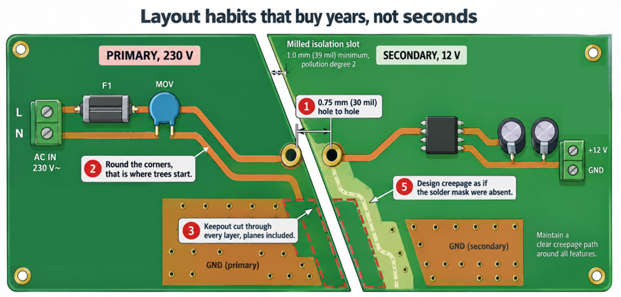
Figure 5: Layout mitigations against slow breakdown, shown on a mains input section
Five layout habits protect a design against the slow mechanisms rather than the fast ones, and none of them cost anything if you apply them at layout time:
- Use two prepreg plies across every high-voltage boundary. A single thin ply can develop a resin-starved region over dense copper, and that region is exactly where partial discharge starts.
- Open the hole-to-hole pitch across the boundary. Filament growth follows glass bundles between plated holes, so 0.5 mm (20 mil) wall-to-wall is a baseline, and 0.75 mm (30 mil) is better above 48 V.
- Round the copper on high-voltage nets. A sharp corner concentrates the field where a tree begins, so replace 90-degree corners with arcs or 45-degree breaks.
- Cut the isolation keepout through every layer. A ground pour reaching the board outline quietly bridges a gap you drew carefully on the top layer.
- Mill a slot when the surface path runs tight. Removing the material removes the creepage path, and IEC 60664-1 wants the groove at least 1.0 mm (39 mil) wide in pollution degree 2.
Contamination control belongs here, too, even though it happens after your part of the job. Flux residue and dust turn a compliant creepage gap into a conductive film. A cleaned and coated board keeps the geometry you designed. Setting PCB voltage clearance per layer and choosing the right prepreg with a tighter weave both help before the board exists.
JLCPCB's High-Voltage Laminates & Manufacturing Capabilities
A fabricator controls two of the variables in this article and none of the others. It supplies the laminate and the lamination quality, while the field, the spacing, and the operating environment all stay with you.
Certified High-Tg and Premium Dielectric Materials Supply Chain
JLCPCB builds standard FR-4 orders on Grade A laminates from Nan Ya, Kingboard, and Shengyi. The JLCPCB certifications page carries the actual datasheets rather than a generic description, so that you can read the numbers yourself. You will find Nan Ya NP-140F and NP-155F, Kingboard KB-6164 and KB-6165F, and Shengyi S1141, S1000H, and S1000-2M.
This matters for a safety file because a specific material grade comes with test data you can verify. Writing KB-6165F in the fabrication notes gives the reviewer a clear reference for its Tg, tracking index, and breakdown performance. Writing only FR-4 does not.
Two things should be confirmed before finalizing the layout:
- CTI: Standard FR-4 is typically a Group IIIa material. A high-CTI grade must be specifically requested and confirmed.
- Polyimide: Rigid polyimide is not normally part of the standard offering; polyimide is generally supplied for flexible PCBs.
Advanced Hi-Pot Testing and Automated Quality Control
Hi-pot testing is not something JLCPCB performs on customer boards, and it is worth saying so plainly. The capabilities pages, the certifications page, and JLCPCB's own high-voltage articles all present hi-pot as advice to the designer. A dielectric withstand test on a finished assembly, therefore, belongs to you or to a compliance test house.
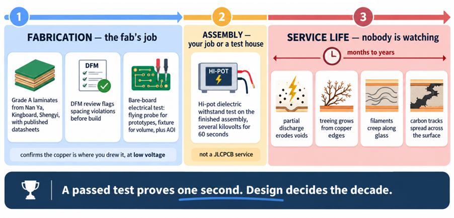
Figure 6: Where fabrication testing ends and lifetime insulation risk begins
What every bare board does get is a full electrical test before it ships. A flying probe handles prototypes, and a fixture handles volume runs, and both drive every net against your netlist. So the test detects open circuits, shorts, and copper slivers between adjacent nets at low voltage: low-voltage isolation testing and a hi-pot test answer different questions. The electrical test confirms that the two nets are separate. Hi-pot confirms that the separation survives several kilovolts, so it answers the question your safety standard actually asks.
FAQs about Breakdown Voltage
Q: My board passed a 3 kV hi-pot. Why did it fail at 400 V two years later?
A hi-pot proves the barrier survives one second of high voltage, so it detects gross defects rather than slow ones. Partial discharge can ignite inside a void at a fraction of that test voltage and erode the resin over months. Conductive anodic filament growth and surface tracking work on the same timescale.
Q: Can I detect partial discharge without a laboratory?
Not reliably. Proper measurement follows IEC 60270, so it needs a shielded setup with a coupling capacitor and a low-noise amplifier. On a bench, a steadily rising leakage current during a withstand test dwell is the most practical warning sign you have.
Q: Does a thicker board give me proportionally more breakdown voltage?
No. Withstand voltage rises with thickness, but the kV/mm figure falls, because a thicker layer contains more voids and glass bundles for a discharge to find. The gap that decides an inner-layer failure is usually one or two prepreg plies of about 0.1 mm (4 mil), not the full board.
Q: Does conformal coating raise my board's breakdown voltage?
It raises surface resistance to tracking rather than the bulk breakdown voltage by keeping moisture and contamination off the laminate. Safety standards will not let you reduce creepage for it unless the coating qualifies under IEC 60664-3. Treat it as protection for the geometry you already designed.
Conclusion
Breakdown voltage reads like a rating and behaves like a countdown. The laminate sets a starting value, and heat, moisture, voids, and surface contamination spend it. None of that spending is visible from outside the board, which is why the failure arrives long after the design review that should have caught it.
The habits that follow are cheap to adopt, because every one of them is a decision rather than a component. Use two prepreg plies across a high-voltage boundary, open the via pitch, and round the copper corners. Design creepage as though the solder mask were absent, and specify the laminate grade instead of writing "FR-4".
As DC-link voltages climb toward 800 V in vehicle and solar hardware, the margin that used to hide these mechanisms is disappearing. A design that survived at 230 V has far less room at 400 V. JLCPCB's published laminate datasheets and DFM checks settle the material half, so your attention can go to the field your layout creates.

Keep Learning
Safeguarding Circuit Boards Against Breakdown Voltage Failure
Key Takeaways Construction Matters: Breakdown voltage depends on stackup and defects, not raw material ratings. Stress Causes Failures: Heat and moisture degrade insulation over time, leading to field defects. Four Main Failure Modes: Insulation fails via internal voids, treeing, CAF growth, or surface tracking. Layout Design Fixes: Use dual prepregs, wider hole spacing, rounded trace corners, and isolation slots. Testing Split: Bare-board testing checks low-voltage net continuity, while hi-pot tests ......
Is FR4 the Best Board Material for Your Design
Key Takeaways Best All-Rounder: Ideal balance of strength, insulation, and low cost for standard PCBs. Clear Limits: Poor heat dissipation (~0.3 W/m·K) and high loss for RF (>3 GHz). Alternatives: Use Rogers for RF, Aluminum for high heat, and FPC for flexibility. Selection Essentials: Pick High-Tg (170°C+) for lead-free reflow and custom stackups for impedance. JLCPCB Advantage: 1–32 layer FR4 boards with ±10% impedance control and 24h fast dispatch. In the world of electronics and printed circuit bo......
Optimizing High-Voltage Circuit Safety with PCB Dielectric Strength
Key Takeaways Non-linear Scaling: Dielectric strength drops as thickness increases. Safety vs Signals: Dielectric strength ensures safety, while Dk controls signal speed. Material Selection: High-voltage safety depends on Tg, CTI, and moisture resistance. Spacing Rules: Clearance prevents air arcs, while creepage prevents surface tracking. Assembly Testing: Hi-pot testing requires finished assemblies, not bare boards. Dielectric strength is the number engineers quote to prove a board is safe at mains ......
How Copper Foil Shapes PCB Performance and Manufacturing Quality
Key Takeaways Weight: 1 oz copper ≈ 35 µm thickness; higher weight increases current capacity. Types: ED for standard rigid boards, RA for dynamic flex circuits. DFM & Loss: Smoother foil lowers RF loss; thicker foil requires wider trace spacing. The part of a PCB that actually carries the electrical signal is the copper foil. The strength comes from the glass weave, the resin is used to keep the layers together, and the solder mask is used to provide protection and separation of exposed copper. But w......
A Complete Guide to Copper Clad Laminate (CCL) in PCB Manufacturing
Key Takeaways CCL is the base material: a cured resin-reinforcement sheet with copper foil bonded to one or both sides. Three parts control performance: Resin affects heat and loss, reinforcement controls stability, and copper foil affects conductor behavior. Choose by the main design stress: Heat, frequency, and cost usually determine the best laminate family. Slash sheets define the material: IPC-4101 uses numbered slash sheets to specify rigid PCB base materials. Tg alone is not enough: Td and time......
Buried Vias in Advanced PCBs: Enabling Higher Density, Better Signal Integrity, and Compact Designs
Key Takeaways Hidden Routing: Buried vias connect only inner layers, keeping outer surfaces clear for dense components and traces. Better Signal Integrity: They eliminate via stubs, reducing parasitics and signal loss in high-speed designs. Higher Density: Essential for HDI boards, dense BGAs, and small form factors like wearables. Higher Cost: Sequential lamination and extra drilling steps make them ~3×-4× more expensive than standard through-holes. Ever wondered how a modern smartphone mainboard can......