
How to Determine the Right PCB Voltage Clearance for Safe and Reliable Designs
13 min
- Why Voltage Clearance Is Critical in PCB Design
- Key Factors Influencing PCB Voltage Clearance
- Practical Guidelines and Standards for Voltage Clearance
- Design Techniques to Achieve Proper Voltage Clearance
- Manufacturing Considerations for High-Voltage PCBs
- JLCPCB's Expertise in High-Voltage PCB Production
- FAQ about PCB Voltage Clearance
- Conclusion
Key Takeaways
- Clearance is the air gap; Creepage is the surface path — both essential for high-voltage safety.
- Base spacing on peak voltage and follow IPC-2221 / IEC 60664-1 standards.
- Major factors: voltage, pollution degree, CTI, altitude, and conductor location.
- Use isolation slots, guard rings, and conformal coating to optimize spacing.
- Always run clearance calculations, DFM checks, and Hipot testing before production.
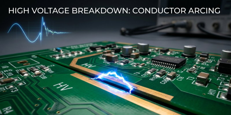
Why do two copper traces that work fine at 5V suddenly arc over and burn at 400V? Well, did the spacing rules change because it's copper? If the PCB Voltage Clearance is not correct, it is the difference between a board that lasts for 10 years and a board that fails as soon as it is powered on. Voltage clearance is the distance between conductors that will not allow the electrical breakdown through air and across the surface of the board. With designs going to higher voltage motor drives, LED drivers, and power supplies.
This separation turns into a mandatory safety issue, rather than a recommendation. Arcing, tracking, and catastrophic failure result from undersized gaps. In this guide, we'll demystify the concepts of PCB voltage clearance, explore the factors influencing it, and discuss its significance. The design and manufacturing techniques to keep your boards safe. At the end, you will be able to use a clearance calculator to get the numbers and use them with confidence.
Why Voltage Clearance Is Critical in PCB Design
All the spaces between each conductor on your board are insulators. Air and the laminate are both insulators, meaning they don't conduct current, but that is, until the voltage is high enough to overwhelm the insulating properties, in this case, the dielectric strength. At that point, you have an arc or slow-blow carbon track that permanently shorts out and stays shorted. That is why there is a voltage clearance for PCBs. The greater the difference in potential (in volts) between two nets, the greater the distance required.
It is not only about keeping sparks out, but also insulation coordination, a method used in standards bodies to ensure a board can handle normal operation and transient overvoltage conditions. In low-voltage digital circuits, clearance is generally not a constraint. However, once mains power, switching supplies, and/or high-side gate drives are involved, clearance is a first constraint that needs to be locked down. Don't ignore it early, or it will create painful re-routes later.
Understanding Clearance vs Creepage and Their Safety Implications
These two terms are often confused, and let's clear that up. The shortest through-air distance between two conductors is called clearance. The shortest path along the surface of the insulating material between those same conductors is termed creepage.
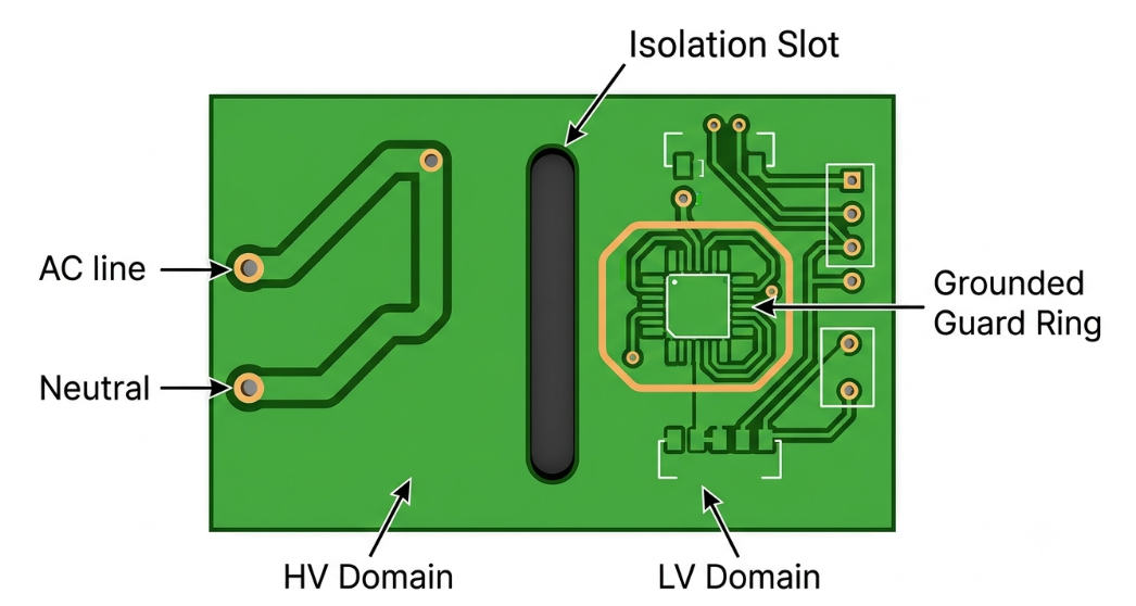
This difference is significant because the two failure mechanisms differ. Clearance is the prevention of air breakdown and arcing for transient spikes. Creepage guards against tracking, which is a conductive carbonized path that will form over the contaminated surface over time. Creepage is always equal to or greater than clearance since a surface path can never be shorter than the straight-line air gap. A slot milled between two traces can drastically affect the creepage without altering the air distance. Later on in the design part, we will be using that trick.
Risks of Insufficient Clearance in High-Voltage Applications
The repercussions are swift if the clearance is too small. A simple design mistake can escalate into a field failure or fire hazard.
- Arc flashover: A transient arc over the gap, which damages components and may hurt the user.
- Surface tracking: Due to the presence of dust and humidity, a leakage path is formed that carbonizes over weeks, reducing the insulation resistance to a short circuit.
- Solder mask breakdown: A thin or porous mask provides a low level of protection; use at high voltage is risky.
- Certification failure: Boards that do not conform to UL or IEC spacing requirements will not gain certification.
Key Factors Influencing PCB Voltage Clearance
No single clearance number can be used for all boards. Reliant on electrical, environmental, and material factors, the required spacing will vary. Knowing these will help you to avoid under-designing (safe but unsafe) and over-designing (safe but a waste of board area). Working voltage, pollution degree, comparative tracking index (CTI) of the material, altitude, insulation type, and circuit classification are the six basic factors that any clearance calculation takes into account. Adjust any of these, and your desired spacing changes.
Voltage Level, Altitude, and Environmental Conditions
The obvious driver is the working voltage, but use the right value. It's usually the peak voltage that clearance is based on, so a 230V RMS mains rail is actually 325V peak. The transient overvoltage categories may cause the design figure to be even higher. The most overlooked variable by engineers is altitude. The higher you ascend, the thinner the air becomes, and the lower the air will break down. Derating of clearance is required above about 2000-3050m according to IPC-2221 and IEC 60664-1.
Material Properties and Pollution Degree Considerations
The laminate surface itself has an effect on the ease of tracking. The Comparative Tracking Index (CTI) measures how a material performs in IEC 60112 and classifies the material in different groups according to the voltage it will track before. The smaller the creepage distance, the higher the CTI. The typical FR4 is in the Group IIIa or IIIb class; the specialized high-Class laminates in the high-CTI class are in Group I for use in high-voltage applications.
Pollution degree is used to indicate the extent of pollution of the operating environment. It can be sealed, dry, zero pollution (Degree 1), normal indoor, occasional condensation (Degree 2), conductive industrial or outdoor wet (Degrees 3 and 4). The greater the pollution values, the greater the creepage required, as the pollution reduces the effective tracking path.
Practical Guidelines and Standards for Voltage Clearance
IPC, IEC, and UL Standards Overview
The standards play different parts in the design and approval process. You don't want to over- or under-apply the rules if you know where they all fit. Printed board conductor spacing, the workhorse is IPC-2221 (Generic Standard on Printed Board Design). It offers Electrical Clearance Tables for voltage and trace position. Refined altitude and coating handling have been added in the current revision IPC-2221C (2023).
IEC 60664-1: The basics of insulation co-ordination for low voltage equipment. It specifies clearance and creepage as a function of the overvoltage category, pollution degree, and material group.
IEC 60112: Prescribes the test method (CTI) to define the material groups.
The UL 60950 / UL 62368-1: product-safety standards (IT and AV equipment), which dictate spacing for certification and are often used to determine the final, binding numbers.
Minimum Clearance Requirements for Different Voltage Ranges
The point is that here is the heart of it, the IPC-2221B electrical clearance table. Values are the minimum spacing for conductors based on the maximum voltage between the conductors and the conductor location. B1: internal conductors, B2: external uncoated (sea level), B4: permanently coated conductors.
| Voltage Range (peak) | B1 Internal (mm) | B2 External Uncoated (mm) | B4 Coated (mm) |
|---|---|---|---|
| 0 - 50V | 0.10 | 0.10 | 0.10 |
| 51 - 100V | 0.15 | 0.15 | 0.10 |
| 101 - 150V | 0.20 | 0.20 | 0.10 |
| 151 - 300V | 0.20 | 0.25 | 0.15 |
| 301 - 500V | 0.25 | 0.50 | 0.40 |
| Above 500V | +0.0025 mm/V | +0.005 mm/V | +0.005 mm/V |
If the voltage is greater than 500V, add the per-volt increment to the base value of 500V. For example, an external uncoated conductor at 580V needs roughly 0.50mm + (80V x 0.005) = 0.90mm. Always check with your end-product safety standard; this will often need more.
Design Techniques to Achieve Proper Voltage Clearance
Routing Strategies, Slotting, and Guard Rings
- Smart routing: Resolves most clearance issues before they occur. Have these techniques on hand:
- Group by voltage domain: Group nets in a "zone" and group components of similar voltage levels together, separated from logic and connectors.
- Mill isolation slots: Machine a slot or groove in the laminate between the high and low voltage areas. The slot provides creepage distance and even a little clearance, allowing you to reduce the footprint.
- Stabilizing guard rings or guard traces: A guard net around a sensitive net has a ground connection that intercepts leakage currents before they can cause issues.
- Avoid sharp corners, increase angles: Sharp corners focus the electric field and promote tracking; chamfer or round high voltage corners on the trace.
Using Clearance Calculators and DFM Tools Effectively
These spacings should not be calculated on each net. An IPC-2221 clearance calculator can do the voltage-to-spacing look-up automatically and will do the per-volt increment above 500V automatically. A good calculator will give you the minimum clearance and creepage, and will take your working voltage (DC or AC peak), conductor location (internal or external, coated or not), and environmental factors such as pollution degree and altitude. Many EDA design-rule checkers allow you to specify these in the form of net-class rules, which means that they are automatically detected when the routing is performed.
Manufacturing Considerations for High-Voltage PCBs
Process Controls to Maintain Clearance Integrity
Clearance if not controlled:
- Etch compensation: More etching increases gaps, less etching decreases gaps, but also makes traces thinner. Controlled Etch Factor Maintains Spacing On Target.
- Layer Registration: If there is a misregistration between layers, then the effective clearance to the adjacent nets may be reduced when it comes to internal conductors.
- Solder mask registration and coverage: When solder clearance values are being used consistently, a void-free solder mask coating (B4) is essential.
- Slot and routing accuracy: Milled isolation slots have to be accurate in order to provide the creepage that they are designed to provide.
- Surface cleanliness: Ionic residue increases surface resistance and will cause tracking, which is important for high voltage products, and cleaning after the surface is produced is important.
For a competent fab, it is easy to keep these tolerances in control, but without the appropriate inspection, they cannot be checked once they have happened. That is why it is a mandatory step, not an option.
Testing and Verification for Compliance
Boards must be installed, and proof of the insulation's performance must be provided. Hipot (dielectric withstand) and insulation resistance are the two most common workhorse electrical tests. A hipot test is a test in which an applied voltage across the isolation barrier is high enough to ensure that there will be no breakdown of the isolation barrier and excessive leakage. Insulation resistance test is used to check leakage at the rated voltage to ensure that the dielectric is in good health. Dimensional inspection, on the other hand, verifies with an automated optical inspection (AOI) that the actual copper spacing is correct in accordance with the design. For products certified to NF, these tests are recorded and linked to the corresponding UL or IEC requirements. Electrical and optical verification means you can be confident that the design and manufacturing were to specification.
JLCPCB's Expertise in High-Voltage PCB Production
Advanced DFM Review for Voltage Clearance Compliance
JLCPCB's DFM (Design for Manufacturing) review automatically checks if the spacing is below the manufacturing and/or specified limits. As you upload your Gerbers, the system automatically alerts you if the copper-to-copper clearance exceeds the capability rules, before any fabrication is done. It is an early feedback loop that is essential when doing high-voltage work. When caught at the quote stage, the marginal AC to DC gap will cost nothing, but if it's caught after a failed certification, it will cost weeks. The DFM report will provide you with a list of clear and actionable changes that you need to make.

Reliable Support for Safe, High-Performance Boards
In addition to the machines, responsive engineering support facilitates high-voltage projects. Quick and easy with JLCPCB's instant online quoting, short 1-2 day turnaround, multiple surface finishes, and SMT assembly, you can prototype and quickly iterate while keeping safety as a top priority. So if you're implementing these clearance rules, JLCPCB's DFM review service and precision manufacturing ensure it is easy to take a safety-compliant design and turn it into reliable hardware that can be certified.
FAQ about PCB Voltage Clearance
Q: What is the difference between PCB voltage clearance and creepage?
Clearance is the shortest through-air distance between two conductors, while creepage is the shortest path measured along the insulating surface between them. Clearance guards against arcing and air breakdown, whereas creepage protects against gradual surface tracking from contamination.
Q: Which standard should I use to determine minimum PCB clearance for high voltage?
Start with IPC-2221 for bare-board conductor spacing, then verify against the end-product safety standard, such as IEC 60664-1 or UL 62368-1. When the values differ, always use the larger spacing to ensure certification compliance.
Q: Does altitude really affect PCB voltage clearance?
Yes. Air becomes thinner at higher altitudes and breaks down at lower voltages, so clearance must be increased above roughly 2000-3050 meters. IEC 60664-1 provides multiplication factors, such as 1.14 at 3000m and 1.48 at 5000m.
Q: How does a clearance calculator work? 1
An IPC-2221 clearance calculator takes your peak working voltage, conductor location, and environmental inputs, then returns the minimum required clearance and creepage. For voltages above 500V, it automatically adds the per-volt increment to the base spacing value.
Q: Can I reduce the required clearance by adding a slot in the PCB?
Milling an isolation slot between high- and low-voltage sections increases creepage distance significantly and adds some clearance, helping you meet spacing rules in compact layouts. However, the through-air clearance requirement for the voltage still applies and must be respected.
Conclusion
Determining the right PCB voltage clearance is not just a technical detail — it is a fundamental requirement for safety, reliability, and regulatory compliance in high-voltage designs. By understanding the critical difference between clearance and creepage, following IPC-2221 and IEC 60664-1 guidelines, and considering real-world factors such as altitude, pollution degree, and material properties, you can prevent arcing, surface tracking, and costly failures.
Proper voltage spacing turns a potential field failure into a long-lasting, certifiable product. Utilize clearance calculators, smart layout techniques like isolation slots and guard rings, and leverage DFM checks early in your design process.
At JLCPCB, we help engineers bring these safe, high-voltage designs to reality with precise manufacturing, professional DFM reviews, and reliable production quality. Start applying these clearance principles today — your next high-voltage board deserves to be both safe and successful.
Popular Articles
Keep Learning
How to Design Your Own Keyboard PCB: From Layout to Firmware
Designing a custom keyboard PCB is one of the most rewarding entry points into practical electronics. You not only get a really useful product on your desk, but also you learn schematic capture, matrix scanning, footprint selection, USB, and firmware. Most of the hardware engineers use the same skills that show up on professional boards. This guide walks the entire build from choosing switches, wiring the diode matrix, adding the microcontroller and USB-C, laying out the board, and flashing QMK or VIA......
Don't Let Design Errors Ruin Your Hardware: The Complete Guide to PCB Design Verification
Key Takeaways PCB design verification is the systematic process of validating layouts against electrical, signal integrity, and manufacturing rules before production, preventing costly board respins and launch delays. Schematic verification through Electrical Rules Check (ERC) catches floating inputs, power shorts, and footprint mismatches before layout begins. Design Rule Checking (DRC) ensures trace widths, clearances, and via sizes comply with your fabricator's manufacturing tolerances, especially ......
How to Determine the Right PCB Voltage Clearance for Safe and Reliable Designs
Key Takeaways Clearance is the air gap; Creepage is the surface path — both essential for high-voltage safety. Base spacing on peak voltage and follow IPC-2221 / IEC 60664-1 standards. Major factors: voltage, pollution degree, CTI, altitude, and conductor location. Use isolation slots, guard rings, and conformal coating to optimize spacing. Always run clearance calculations, DFM checks, and Hipot testing before production. Why do two copper traces that work fine at 5V suddenly arc over and burn at 400......
Mastering PCB Footprints: Design Best Practices for Reliable Manufacturing
Key Takeaways A PCB footprint (land pattern) translates component datasheet dimensions into copper pads, solder mask openings, paste apertures, silkscreen, and clearance areas that enable reliable soldering and assembly. Follow IPC-7351 standards and manufacturer DFM rules for pad dimensions, spacing, and layer design to minimize defects like solder bridging, tombstoning, and cracked joints. Choose between through-hole (THT) and surface mount (SMT) footprints based on electrical needs, thermal perform......
How Copper Thieving Balances Your PCB for Better Manufacturing Results
Key Takeaways Copper thieving adds non-functional copper patterns (dots, squares, or crosshatch) to balance copper density across PCB layers. This effectively reduces uneven plating (from 20-30% to <10%), board warpage, inconsistent etching, and impedance issues, delivering tighter tolerances, better solder mask adhesion, higher yields, and lower costs. For best results, target 40-60% copper density per layer, maintain proper clearances, and ensure stackup symmetry. When done right, it transforms comp......
ZIF Connectors Simplify Flexible PCB Assembly with Tool-Free Reliability
Did you ever attempt to mate a fragile flex cable into a connector and experience that unpleasant resistance, and wonder whether you were tearing off the tail or breaking the casing? It is precisely that tension that the ZIF connectors were supposed to help remove. Zero insertion force technology allows you to slide a flexible printed circuit or flat flexible cable into the receptacle to be mated with, using almost no push force at all, but rather allows a mechanical actuator to hold the cable firmly ......