A Practical Guide to ODB Files for PCB Manufacturing
16 min
- What Is an ODB File?
- Understanding the ODB File Format
- How an ODB File Works in PCB Manufacturing
- ODB File vs. Other PCB Manufacturing Data
- Preparing an ODB File for Production
- How Professional PCB Manufacturers Handle ODB Files
- FAQ About ODB Files
- Conclusion
Key Takeaways
- All-in-One Data: ODB++ combines artwork, netlist, stackup, and drill spans in a single package.
- Fewer Errors: Embedded netlists allow CAM software to catch errors before production.
- Pre-Export Checks: Clear DRCs, close the board outline, and verify drill spans in a viewer.
- Best Practice: Use Gerber for quick quotes and keep ODB++ ready for engineering queries.
A Gerber layer might simply say, “draw a 0.5 mm (20 mil) circle here.” ODB++ can describe that same feature as a pad on the VCC net, connected to a plated hole running from layer 1 to layer 4. In other words, the fabricator receives a description of the board, not just a set of drawings.
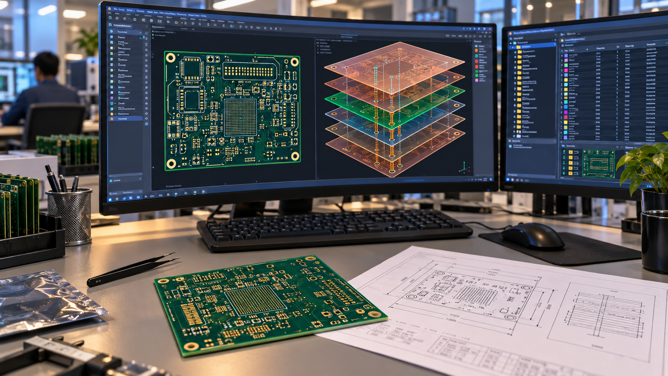
Figure 1: A CAM engineer reviewing an imported ODB++ job
That matters because every assumption the fab has to rebuild from separate files creates another chance for error. When the original design objects and relationships are included, DFM tools can check the board against its own netlist, stackup, drill definitions, and component data. This guide explains what an ODB++ file contains, how its folder structure is organized, and how it compares with modern Gerber and IPC-2581. It also covers the checks worth making before export, so when a fabricator asks for manufacturing data, you know which format to send and why.
What Is an ODB File?
Designers say ODB file, layout tools export ODB++, and both names point to one package of manufacturing data.
What Is an ODB File and What Is It Used For?
An ODB file is a complete manufacturing database for a printed circuit board. It can contain the copper artwork, drill data, netlist, stackup information, and component placement in one structured package. Technically, it is not a single file at all. The data is stored in a folder hierarchy that is usually compressed before it is sent to the manufacturer.
That structure replaces the loose collection of files used in a typical Gerber order. A Gerber package may include a dozen artwork files, one or more drill files, a stackup PDF, and a readme. Each file contains useful data, but very little inside the package explains how those files relate to one another. ODB keeps that information connected. Fabrication uses the layer artwork and drill definitions, assembly uses placement and component data, test uses the netlist, and DFM tools can read the same job structure. One export can therefore support several manufacturing stages without requiring a separate file set for each one.
ODB File and ODB++ in PCB Data Exchange
ODB stands for Open DataBase, and ODB++ is the version everyone actually uses. Valor Computerized Systems released the original ODB format in 1995 and extended it into ODB++ soon after. ODB++ is not a committee standard, since one company defines what each new release contains. Joining the ODB++ Solutions Alliance costs nothing, and the interfaces are supplied to CAD and CAM vendors at no charge. Siemens also gives away a viewer. That is why the format spread so widely through the fab side of the industry.
The family splits into three modules, and only one concerns a designer. ODB++Design carries the product data you export from your layout tool. ODB++Process and ODB++Manufacturing describe factory floor information, so both sit downstream of your order. When a fab asks for an ODB file, it means an ODB++Design job, which belongs to the wider family of PCB file formats alongside Gerber and IPC-2581.
Understanding the ODB File Format
An ODB++ job is a directory tree rather than a document, so the structure is the format. Once you know which folder holds what, you can open one and inspect it yourself.
How the ODB File Format Organizes PCB Data
Everything in an ODB++ job sits inside one main folder with a defined set of subdirectories. Because the structure is standardized, CAM software can understand a job without relying on custom file names. After unpacking the archive, you will typically see folders such as matrix, steps, symbols, wheels, fonts, and misc.
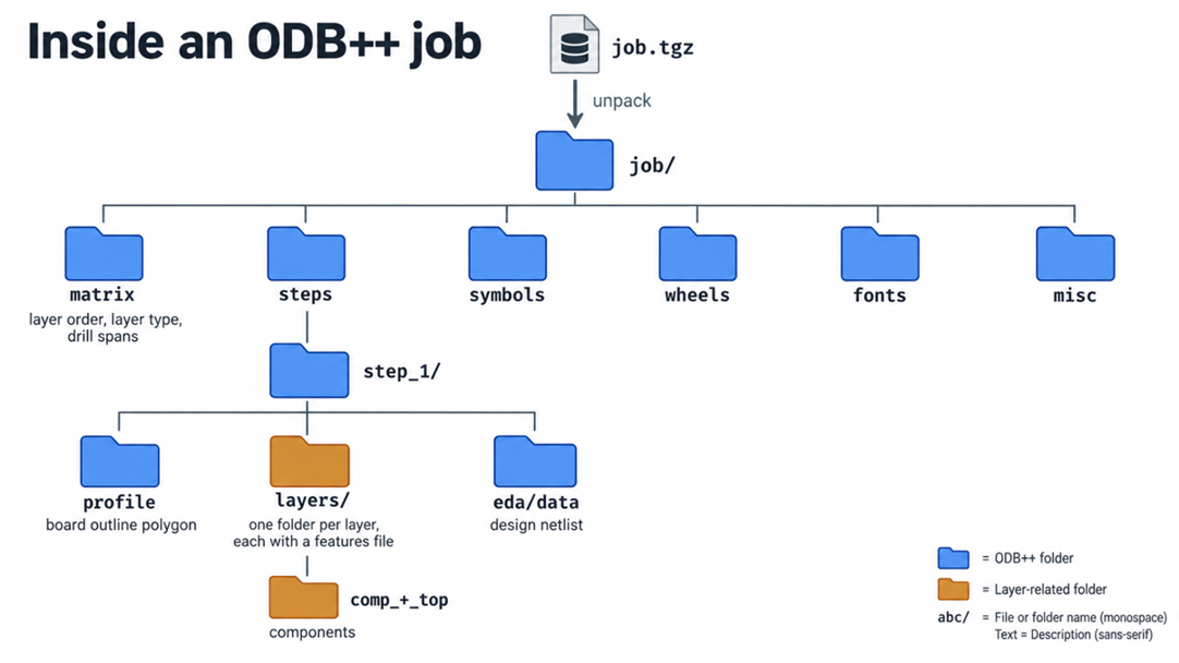
Figure 2: The directory hierarchy of an ODB++ job
The matrix is one of the most important parts of the job. It lists every layer in physical order, identifies the purpose of each layer, and defines the start and end layers for each drill span.
| Path Inside the Job | What It Holds | Why the CAM Engineer Needs It |
|---|---|---|
| `matrix/matrix` | Layer order, layer type, and the start and end layer of each drill span | Rebuilds your stackup with no separate readme |
| `steps/<step>/profile` | The board outline is a closed polygon | Fixes the routed shape, so nothing is traced from a drawing |
| `steps/<step>/layers/<layer>/features` | Every pad, line, arc, and surface on that layer, each with its attributes | The artwork itself, tagged by what each shape is for |
| `steps/<step>/eda/data` | Net names and the features belonging to each net | Let's compare your netlist against the finished artwork |
| `steps/<step>/layers/comp_+_top` | Reference designators, part numbers, and placement for the top side | Feeds assembly programming and pick and place |
| `symbols`, `wheels`, `fonts`, `misc` | Reusable shapes, aperture definitions, text fonts, and job information | Keeps the features files compact and the job self-describing |
What PCB Information Can an ODB File Contain?
Artwork is only the first of six data types inside the job. Everything else is there because manufacturing needs more than shapes. Each item removes a question the fab would otherwise have to email you about.
- Feature attributes: Individual pads, lines,s and surfaces carry labels marking them as a test point, a fiducial, a via pad, or a surface mount pad.
- The design netlist: Net names plus the features on each net, which is what makes an automatic comparison against the artwork possible.
- Stackup and drill spans: Layer order, material names, and the exact start and end layer of every drilled hole.
- Component data: Reference designators, part numbers, and placement coordinates for both sides of the board.
- The board profile: The outline is stored as a closed polygon, rather than as a drawn line on a documentation layer.
- Multiple steps: The single board, the assembly array, and the production panel, all inside one job.
Exporting to Gerber strips away much of that design intelligence because the format was originally created to drive photoplotters, not to describe the full PCB as a connected product.
How an ODB File Works in PCB Manufacturing
Your ODB file never reaches a drill machine or an imaging head. It reaches CAM instead, so what the factory floor runs is data generated from your job rather than the job itself.
From ODB File to PCB Production Data
CAM preparation follows a similar sequence at most PCB fabs. The engineer may use Siemens Valor Process Preparation, Frontline InCAM, or Ucamco UcamX, but the workflow is still built step by step, with each stage depending on the one before it.
That makes early checks especially important. A problem caught at the start can prevent errors from carrying into panelization, tooling, test, and fabrication data later in the process.
- Import the job and rebuild it as an internal CAM database, keeping the layer roles and drill spans from the matrix file.
- Extract a netlist from the artwork and compare it against the netlist you supplied, since that is the check that finds corrupted data.
- Run DFM analysis against the fab's own process limits, covering annular ring, spacing, mask sliver,s and acid traps.
- Panelise the job by stepping and repeating the board, then add rails, fiducials, tooling holes, and any test coupons.
- Generate the outputs: imaging data, NC drill and rout programs, AOI reference images, the electrical test program, and stencil data.
The factory does not run your original design file directly. It first converts that data into the machine files used for imaging, drilling, routing, inspection, and testing.
Using ODB Files for Multilayer and High-Density PCBs
Layer count is where implicit manufacturing data becomes risky. A two-layer PCB has only one drill span, so there is little room for confusion. A ten-layer HDI board may have laser microvias from layer 1 to layer 2, buried vias from layer 2 to layer 9, and through-holes across the full stack. The drill data now represents several different layer spans.
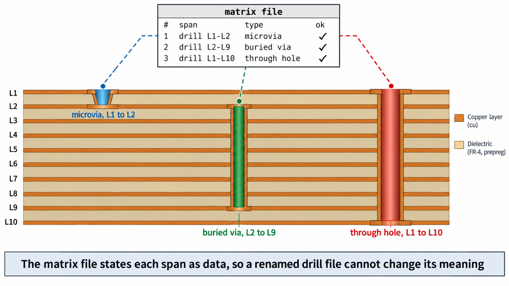
Figure 3: Drill spans on an HDI stackup as declared in the ODB++ matrix file
Gerber usually handles this through naming conventions. You might provide separate drill files called L1-L2.drl, L2-L9.drl, and L1-L10.drl, leaving the fab to interpret the span from the filename.
ODB++ stores that information directly in the matrix. Each drill span is defined as part of the job data, so changing a filename does not change what the hole means. This becomes even more important with sequential lamination, where buried vias are drilled and plated before additional layers are pressed on.
ODB File vs. Other PCB Manufacturing Data
Gerber has moved a long way since RS-274X, so the old claim that it carries only dumb pictures is out of date.
ODB Files and Gerber Files
RS-274X, still called Gerber X1, is pure geometry plus aperture definitions. Gerber X2 added attributes in 2014, so a file can now declare that it is the top copper layer. Attributes also mark a pad as surface-mount and name the net that a feature belongs to. Gerber X3 went further again by adding component layers, which lets footprints, placement, and part numbers travel in the Gerber family too.
Gerber also stays easier in one way that counts. Any viewer opens it, any tool writes it, and a single layer can be inspected on its own. So it remains the default upload format almost everywhere, which is why preparing a clean Gerber set is still the most useful file skill a designer can have.
| Format | What It Carries | Choose It When | What to Actually Send |
|---|---|---|---|
| Gerber RS-274X (X1) | Geometry and apertures only, one file per layer, drill data separate | You want the safest, most universally readable option | The artwork and the Excellon drill file are zipped together |
| Gerber X2 | X1 plus layer function, pad usage, and net attributes | Your CAD tool writes them, and your fab reads them | Confirm the fab uses the attributes before relying on them |
| Gerber X3 | X2 plus component layers, footprints, and part numbers | Assembly data should stay in the same file family | Still pair it with a BOM and a centroid file |
| ODB++ | Artwork, netlist, stackup, drill spans, and components in one job | Multilayer or HDI works with a fab that asks for it | The `.tgz` job, plus a Gerber set if you order online |
| IPC-2581 | The same breadth as ODB++, held in one open XML file | You want vendor-neutral data and a committee standard | Check that your fab's parser supports Revision C |
Why Structured Manufacturing Data Matters
Structure is what makes verification possible at all. A fab can check a geometry-only file against its own process rules. It cannot check that file against your intent, because your intent was never sent. Add a netlist, and the same data becomes testable against itself.
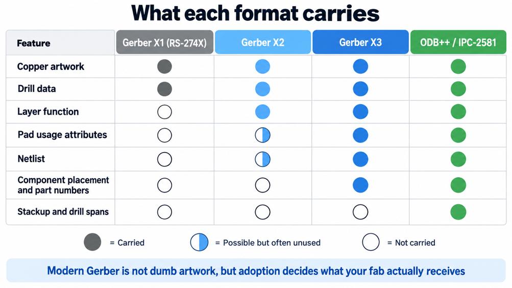
Figure 4: Side-by-side comparison of Gerber, ODB++ and IPC-2581 data content
IPC-2581 is the open answer to the same problem. Published by IPC and also known as IPC-DPMX, it packs artwork, stackup, netlist, BOM, and assembly data into a single XML file. Choosing between the two is less a technical decision than a political one. ODB++ is controlled by Siemens and has deep roots in the CAM software that fabs already run.
Preparing an ODB File for Production
A complete ODB file is not automatically a buildable one. Export quality and manufacturability are separate problems, so both get checked before your board reaches a drill.
Design Checks Before Exporting an ODB File
The exporter copies your design faithfully, mistakes included. So the checking has to happen before you click export. Work through this sequence in your layout tool, because each item is something CAM cannot resolve without asking you first.
- Run a clean design rule check and clear every violation, including the ones you have been ignoring since revision one.
- Draw the board outline as a single closed polygon on the layer your tool designates for it.
- Confirm the layer stack assignment and the physical layer order in the export dialog rather than trusting the default.
- Give real names to the nets that matter, since a mismatch report is only useful if you can read the net names in it.
- Verify every drill span, especially blind and buried pairs, against the intended stackup.
- Open the exported job in a free ODB++ viewer before you send it anywhere.
DFM Requirements for Reliable PCB Fabrication
Manufacturability is judged against the fab's real process limits, never against your file format. The numbers below are JLCPCB's standard capabilities, and they are typical of high-volume prototype fabrication generally.
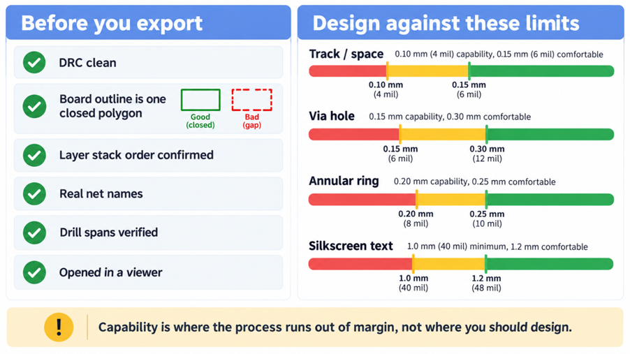
Figure 5: Pre-export checklist and DFM limits for PCB manufacturing data
| Feature | Standard Capability | Comfortable Design Value | What Happens Below It |
|---|---|---|---|
| Track width and spacing, 1 oz copper | 0.10 mm / 0.10 mm (4 mil / 4 mil) | 0.15 mm (6 mil) | Track tolerance of plus or minus 20% eats your whole margin |
| Via hole and via pad | 0.15 mm hole, 0.25 mm pad (5.9 mil / 9.8 mil) | 0.30 mm hole, 0.50 mm pad (11.8 / 19.7 mil) | Drill wander can break the barrel out of the pad |
| Plated through-hole annular ring | 0.20 mm (7.9 mil) | 0.25 mm (9.8 mil) or more | Breakout leaves a partial ring and a weak plated barrel |
| Solder mask bridge, 1 oz copper | 0.10 mm (4 mil) | 0.12 mm (4.7 mil) | The dam fails to print, so adjacent pads share one opening |
| Silkscreen text height | 1.0 mm (40 mil) | 1.2 mm (47 mil) | Characters blur, clip, or disappear entirely. |
How Professional PCB Manufacturers Handle ODB Files
Whatever format arrives, the factory converts it into one internal job and then works from that copy.
Engineering Review and Manufacturing Data Verification
Engineering review is the first real checkpoint. Your job is important, the netlist is checked, and the design is compared against the manufacturer’s process capabilities. Anything that does not pass becomes a customer query, and even a simple query can add a day or more to the lead time. Knowing what your manufacturer’s front end accepts helps avoid that delay. JLCPCB’s published file-format guidance lists RS-274X, Gerber X2, IPC-2581, and ODB++ among the CAD outputs it supports.
Treat the two exports as serving different purposes. Send the Gerber set with the order, because that is what the quoting system reads and renders for review. Keep the ODB++ job available, and provide it if a question comes back about a drill span, layer structure, or netlist. JLCPCB’s Gerber export guide also covers the required settings for different PCB design tools.
Fabrication, Inspection, and Quality Control
Everything the factory inspects is derived from the data you sent. Automated optical inspection compares the etched copper against a reference image built from the CAM job. A feature that was wrong in your file is therefore equally wrong in the reference. Inspection proves the process matched the data, not that the data was correct.
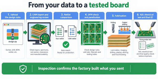
Figure 6: The path from design data to a tested PCB inside a manufacturer
An electrical test is where a supplied netlist earns its keep. A flying probe or a bed of nails checks every net for continuity and every net pair for isolation. To do that, it needs a list of what should connect to what. Final quality control closes the loop with dimensional checks, visual inspection against IPC-A-600 Class 2 criteria, and impedance coupon measurement, where the order calls for it. Inspection can only confirm that the factory built what you sent.
FAQ About ODB Files
Q: Is an ODB file the same thing as an ODB++ file?
In everyday use, yes. ODB was the original 1995 format from Valor Computerized Systems, and ODB++ is the extended version that modern tools read and write. When someone says ODB file, they almost always mean an ODB++ Design job.
Q: Can I open an ODB file to check it before sending it?
Yes, and you should. Siemens supplies a free ODB++ viewer, and most CAM and layout packages can import a job as well. The archive also unpacks into ordinary folders whose feature files are plain text, so you can confirm the layer list by hand.
Q: Should I send ODB++ or Gerber to my PCB manufacturer?
Send whatever the ordering system parses, which for most online fabs, including JLCPCB, means Gerber RS-274X plus an Excellon drill file in a single zip. Keep the ODB++ job available for engineering queries about drill spans, netlists, or stackup, where it answers faster than an email chain.
Q: Does an ODB file replace my fabrication drawing?
Not entirely. The job carries stackup, drill span,s and netlist data. Requirements such as surface finish, solder mask color, impedance tolerance, and special process notes are not all reliably captured, so attach a fabrication drawing alongside it.
Q: Is ODB++ better than IPC-2581?
They carry comparable information, so the practical difference is governance and support. ODB++ is owned by Siemens and is deeply embedded in fab CAM software, while IPC-2581 is an open committee standard.
Conclusion
An ODB file is best understood as a shift in what you are sending. Gerber hands the factory a set of pictures and asks it to work out the product behind them. ODB++ hands over the product description directly, so pads stay pads and nets stay nets. A buried via span becomes a stated fact rather than a naming convention.
Verification is what that shift really buys you. Once the netlist travels with the artwork, CAM can verify that the two agree, so mistakes surface during review rather than during electrical testing. Export Gerber for the ordering system that your manufacturer actually parses. Keep an ODB++ or IPC-2581 job ready for the engineering questions that follow. Then check your outline, netlist, and drill spans before either file leaves your machine, since JLCPCB's instant DFM preview can only report what you gave it.

Popular Articles
• AI PCB Design: From Prompt to PCB with EasyEDA Pro
• AI Tools for PCB Design: Which Tool Fits Your Workflow Stage?
• GPT-6 Astra PCB Design in KiCad: From Brief to Verified Native Project
• GPT-6 Astra PCB Design in EasyEDA Pro: What Worked, What Failed, and What We Learned
• How to Design Your Own Keyboard PCB: From Layout to Firmware
Keep Learning
AI Tools for PCB Design: Which Tool Fits Your Workflow Stage?
AI tools can now assist with PCB architecture, schematic generation, component selection, placement, routing, and design verification. However, different tools target different stages of the PCB workflow. This guide compares AI tools for PCB design based on what they actually do, what inputs they require, and where they fit within a real engineering workflow. In this guide, you will learn: The 6 types of AI PCB tools and the input each one needs What AI PCB design tools do, compared stage by stage How......
Free Online Circuit Simulator for Electronics Engineers
Key Takeaways Simulate First: Free circuit simulators prevent fried components and cut PCB re-spins. Fix AC Sweep: Enter pure numbers for points per decade, not time units. Use SMD Parts: Swap ideal models for standard SMD resistors and SOT-23 transistors. Control Parasitics: Board trace capacitance and via inductance alter high-frequency signals. Verify Before Order: Pair SPICE simulation with DFM checks to ensure board success. If all electronic engineers had a dollar for each burnt-out resistor or ......
Mastering PCB Design Rules: A Comprehensive Guide for Optimal Results
Key Takeaways Follow core PCB design rules for reliable electrical and mechanical performance. Optimize trace width, spacing, impedance, and vias for signal integrity and manufacturability. Apply DFM and DRC early to identify potential manufacturing and layout issues. Consider thermal management, grounding, and testing during the PCB design stage. Align design rules with your PCB manufacturer’s capabilities to improve production reliability and reduce redesigns. PCB design rules are essential guidelin......
KiCad MCP: How to Design a PCB with Claude Code [Step-by-Step]
Key Takeaways Claude can design PCBs in KiCad: By connecting Claude to KiCad through an MCP server, you can use AI to create and modify PCB designs. In this project, Claude helped turn a 5 A XL4015 buck converter netlist into a two-layer, 63 × 33 mm PCB layout with zero ERC violations and zero DRC errors after minor initial fixes. Set up Claude securely: Use a KiCad MCP server that starts in read-only mode. Review the server code before installing it, connect through stdio, and allow editing only in a......
Claude Code PCB Design: Can It Build a Real Board in EasyEDA Pro?
Key Takeaways Claude Code PCB design: Using Claude Opus 5.5 and EasyEDA Pro 3.2.149, I converted a 47-component, three-page schematic from a PDF into a fully routed, two-layer PCB with zero DRC errors. EasyEDA Pro integration: The EasyEDA API skill connects Claude Code to EasyEDA Pro through a local bridge server and the Run API Gateway extension. This allows Claude to control the editor via JavaScript, with a 30-second timeout per API call. Design verification: A successful API response doesn't alway......
How to Design a PCB with Flux.ai (Step-by-Step Guide)
Key Takeaways This step-by-step Flux PCB design tutorial demonstrates the complete workflow by creating a compact 15 × 15 mm USB 2.0 hub, refining the layout, routing high-speed differential traces, and preparing manufacturing files for JLCPCB PCB fabrication and assembly. We are all hearing news; new AI models are being released every month. And it has finally reached the schematic editor. Flux.ai is a browser-based AI PCB design tool with a built-in AI agent that behaves like a junior hardware engin......