Guardians of Quality: A Complete Walkthrough of PCB Inspection Standards
17 min
- Foundations of Quality Assurance in Circuit Board Fabrication
- Comprehensive Breakdown of Common Inspection Methods
- Critical Defects Identified During Industrial Checkpoints
- Systematic Execution: The Core PCB Inspection Steps
- Why JLCPCB Sets the Benchmark for Automated Inspection Excellence
- FAQ about pcb inspection
- Conclusion
Key Takeaways
- Layered Defense: Combining AOI, AXI, ICT, and FCT covers all inspection blind spots.
- Paste Printing: Solder paste causes up to 60% of defects, making early checks vital.
- IPC Standards: IPC Class 3 tightens BGA void limits from 25% to 10%, raising costs.
- Thermal Balance: Equal layout heating balances reflow pull to prevent tombstoning.
- Design Control: Clear test pads and visible polarity marks ensure reliable automated checks.
PCB inspection is not one check performed at the end of production. It combines inspections and tests, with each stage targeting problems that the others may miss. AOI quickly finds visible soldering defects. However, it cannot see joints hidden beneath a BGA. X-ray inspection reveals those hidden connections, yet it still cannot confirm whether the assembled board powers up and works as intended. That is why reliable PCB inspection depends on using the right methods at the right stages.
In this guide, you will learn:
- What PCB inspection covers, from bare board to finished assembly
- How AOI, X-ray, ICT, and functional test differ
- The solder joint defects behind the field returns
- How much voiding inside a solder ball is allowed
- What changes at Class 3 instead of Class 2
- Which step catches which defect, and what none of them catch
Foundations of Quality Assurance in Circuit Board Fabrication
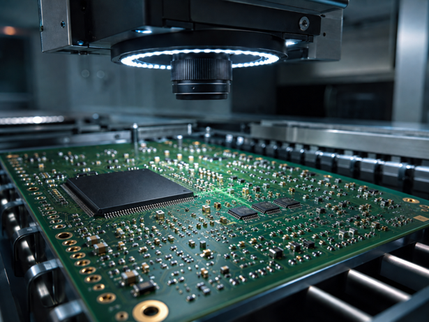
A finished assembly sits sealed inside its housing. You can photograph and X-ray the outside, but you cannot open it to inspect a joint beneath a ball grid array. Inspection, therefore, combines methods, allowing each field of view to cover the blind spots left by another method.
What is PCB Inspection and Why It Matters in Modern Electronics
PCB inspection is a set of checks confirming that a board matches its design files and an agreed workmanship standard. These checks occur at fixed points, from bare copper through a powered assembly. Each one measures a different physical property: shape, density, resistance, or behavior. Two standards divide this work; confusing them creates avoidable disputes with suppliers.
- IPC-A-600 covers the bare board: copper, laminate, plating, mask, and legend.
- IPC-A-610 covers the assembled board: solder joints, placement, and cleanliness. The current revision is IPC-A-610J, published March 2024.
- IPC J-STD-001 sits alongside it and covers the soldering process and materials.
The need for inspection increases as the years go by because packages cover up their joints. For instance, the RP2040 is delivered in a QFN-56 package, 0.4 mm (16 mil) pin pitch with a thermal pad under the body. An 0201 chip resistor is 0.6 x 0.3 mm (24 x 12 mil) and is approximately the size of a coarse grain of sand, and neither joint can be seen by a person holding a magnifier.
The Direct Correlation Between Rigorous Testing and Field Reliability
Inspection does more than sort good boards from bad. It confirms that the process remains under control, because the most damaging defects are those that pass unnoticed on the day of production.
A cracked joint may conduct perfectly at 25 degrees C on the bench, then fail in a car engine bay cycling between -40 and +125 degrees C as the temperature repeatedly opens and closes the crack. Solder paste printing is the largest single source of assembly defects; commonly cited figures assign 30 to 60% of defects to this step. A deposit at 60% of the target volume is easy to reprint, but after reflow, that shortfall becomes a starved fillet buried beneath the package.
Where the board lives decides how much this matters. A phone in a pocket sees gentle thermal cycles and almost no vibration. A drone flight controller sees constant vibration and a 60-degree swing every flight.
Comprehensive Breakdown of Common Inspection Methods
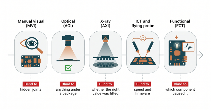
Five methods handle almost every inspection task on a production line. Each measures a different physical quantity, giving every method a distinct blind spot.
| Inspection Method | What It Measures | What It Catches Best | What It Cannot Reach |
|---|---|---|---|
| Manual visual (MVI) | Reflected light, judged by a person | Damage, labels, and connector seating | Hidden joints, pitch under 0.5 mm (20 mil) |
| Optical (AOI) | Reflected light against a reference image | Missing, offset, or reversed parts | Any joint under a package body |
| X-ray (AXI) | Absorption through the solder | Voids and opens under BGA and QFN | Whether the right value was fitted |
| ICT and flying probe | Resistance, capacitance, junction voltage | Wrong value, reversed polarity, shorts | Speed, firmware, calibration |
| Functional (FCT) | The board's outputs while powered | Anything that stops the product from working | Which component caused it |
Manual Visual Inspection (MVI) and Automated Optical Inspection (AOI)
Manual Visual Inspection is combining a trained operator with magnification and the reference pictures in IPC-A-610. Still, there's a place for humans to check connector seating, mechanical hardware, labels, and minor irregularities that render a board unacceptable when it should be.
The only thing human inspection can see is repetition and fine detail. Detection reliability may be reduced during an extended shift, and work becomes more difficult below about 0.5 mm (20 mil) pitch. AOI fills that gap. Automated Optical Inspection (AOI) takes a picture of the board under controlled lighting. It then compares each region with a reference that is created from the CAD data or from a known good first article. The system flags:
- Missing components, the most common find of all
- Offset and rotation, measured in fractions of a pad
- Reversed polarity, read from the body marking or cathode band
- Bridges, excess solder, and insufficient fillets, where 3D AOI measures joint height rather than brightness
A related machine works before reflow: solder paste inspection (SPI). It uses a light pattern to scan the printed solder paste and checks each deposit for height, area, volume, and position.
Advanced Structural Analysis via Automated X-ray Inspection (AXI)
X-ray inspection works because solder is denser than most other board materials. Tin, lead, and silver absorb the beam strongly. Plastic, silicon, and FR-4 transmit more of it, making each joint appear dark while the package body fades into the background.
Three imaging modes exist:
- 2D transmission captures one straight-through image quickly, but far-side parts can overlap near-side features.
- 2.5D oblique tilts the source or board so that overlapping features separate.
- 3D tomosynthesis or CT reconstructs angled images as slices, letting you view one layer at a time. It is slower, but gives the clearest result on dense assemblies.
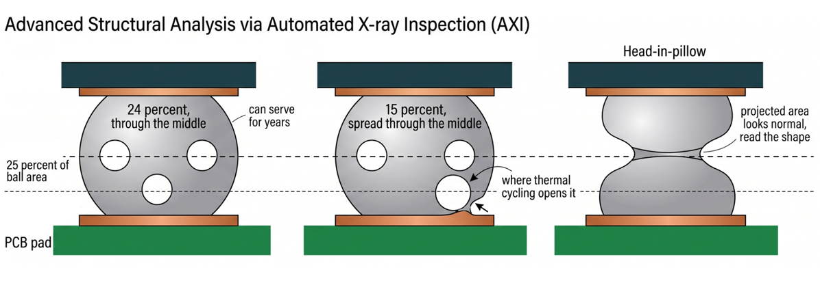
IPC-7095 treats a solder ball as defective when the projected area of all voids exceeds 25 percent of the ball area in the X-ray image. Many high-reliability programs write around 10 percent into their own specification, which is common Class 3 practice rather than a standard requirement.
A field failure exposed the risk: A batch of drone flight controllers passed AOI and shipped. Eleven returned within two months because the inertial sensor dropped out during flight. X-ray showed each corner joint of the 0.4 mm (16 mil) pitch package as two masses joined by a narrow waist, not one fused ball. The package bowed at peak reflow, lifting the corner balls from the paste before the two could fuse.
That defect is head-in-pillow, which is why operators judge shape rather than area. Its projected area appears normal. The defect concentrates at package corners where warpage peaks, yet passes a room-temperature continuity check because the two halves remain in contact.
Electrical Continuity Verification: In-Circuit Testing (ICT) & Flying Probe
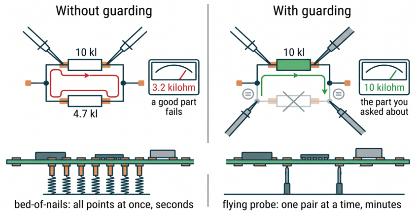
In-circuit testing is the testing of individual components on a populated board without removal. This might sound like an impossible task, as each component is part of a network. The tester rejects a good part when it reads a 10-kilohm resistor with a parallel 4.7-kilohm path as 3.2 kilohm. The tester overcomes this by putting additional probes at nodes adjacent to the parallel path. It maintains the same potential as one end of the part being tested at these nodes. There is no voltage across that branch; therefore, no current flows through it, and the meter reads just the intended component.
This technique checks many features within seconds on each board:
- Resistor, capacitor, and inductor values are typically within a few percent
- Diode and transistor junction drops, which are how the reversed parts get caught
- Shorts and opens on every net with a probe point, plus rail voltages on some testers
Commonly cited figures place ICT coverage between 70 and 90% of manufacturing defects, more than any other single method described here.
A flying probe takes the same measurements differently. Two to eight probe heads ride on gantries and touch pads, one pair at a time. No fixture is needed, which is why prototypes go this way, and the cost is time: a bed-of-nails contacts every point at once in seconds, while a flying probe works serially and takes minutes. Our guides to flying probe testing and bed-of-nails testing cover when each earns its keep.
Final Performance Validation with Functional Test (FCT)
Functional test powers the board, operates it as the finished product would, and compares its outputs with defined pass and fail limits. It is the final gate before enclosure and the only method that tests the board as a complete system, not merely as individual parts. FCT therefore catches failures where every component is correct, but the assembled board still fails:
- An oscillator that starts at 25 degrees C and refuses at 0 degrees C
- A regulator that is stable, unloaded, and rings under 500 mA
- A joint that conducts cold and opens once the board warms
FCT tells you the board failed, not which of 400 components did it. Where there is no room for test pads, boundary scan over JTAG bridges that gap by shifting patterns through the pins of the ICs themselves. Your assembler needs your specification, fixture, and firmware to run a functional test. FCT is the one inspection gate that you must design.
Critical Defects Identified During Industrial Checkpoints
Defects divide according to when they form. Bare board defects come from fabrication chemistry and drilling; assembly defects come from solder paste, component placement, and reflow.
Surface and Layer Imperfections: Key Defects Checked in Bare Boards
Finding bare board defects before fitting components keeps their correction inexpensive:
- Copper slivers and etch shorts, bridging nets that should never meet
- Opens from a scratch in the etch resist, thinning a trace until it breaks
- Voids in a plated barrel, invisible from both faces, are findable only with the current
- Annular ring breakout, where the drill wandered past its pad
- Solder mask on a pad, an open joint assembly cannot be soldered
- Measling and delamination, resin separating from the glass weave
- Oxidation of the finish, a condition that cameras and electrical probes cannot detect
Assembly and Solder Joint Anomalies: Micro-Shorts, Voids, and Tombstoning
After component placement, most defects trace to three variables: how much paste was printed, where the part landed, and how evenly heat reached both ends. Four defects account for most rework:
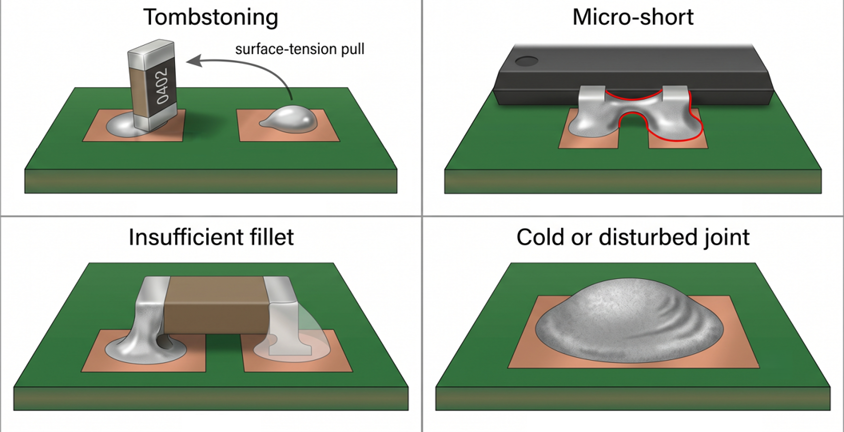
- Micro-shorts: Solder connects adjacent leads after excess or slumped paste spreads at fine pitch. AOI finds visible bridges; AXI detects those hidden under packages.
- Insufficient fillet: A thin, concave joint forms when a deposit is starved, or an aperture is blocked. SPI catches the shortage before reflow; 3D AOI measures its finished height.
- Cold or disturbed joint: A dull, grainy joint forms because the component moved before the solder solidified. AOI flags its appearance; FCT finds joints that open once hot.
- Tombstoning: A chip part standing on one end. Caught by AOI, prevented by layout.
Tombstoning begins with a wetting imbalance, where molten solder exerts a greater pull on one end than the other. This published work determined that the tombstone rate increases from about 0.02 percent to 1.8 percent when the pad overhang is more than approximately 0.07 mm (2.8 mil) different between the ends on a 0402 chip component. Maintain a difference of 0.05 mm (2 mil) or less.
Three layout mistakes cause most of the rest:
1. Heat imbalance: Tying one pad of the footprint into a copper pour and the other into a thin trace. The pour drags heat away, so that end melts late while the other has already wetted and started pulling. Correct this by giving both pads the same thermal connection.
2. Tight spacing: Placing 0201 parts below your assembler's minimum spacing. Adjacent deposits merge into a bridge during reflow. Correct this by checking the spacing rules for your tier before routing.
3. Hidden marks: Putting the polarity mark beneath the component hides it. AOI compares the printed marking against the part it can see. Correct this by moving pin 1 dots outside the outline.
Systematic Execution: The Core PCB Inspection Steps
The complete PCB inspection sequence has two halves. Fabrication checks copper and laminate before component placement; assembly checks solder joints and circuit behavior afterward.
Pre-Lamination and Post-Etching In-Line Quality Gates
Fabrication uses a chain of quality gates, each positioned at the final stage when its target defect remains reachable:
- Inner layer AOI after etching and before lamination.
- Post-drill and post-plate checks on hole position, size, and barrel copper.
- Outer layer AOI after pattern plating and etching.
- Solder mask and legend registration against the pads.
- Bare board electrical test against the net list.
- Final visual and dimensional QA on outline, thickness, and warp.
Once the stack goes into the press, an inner-layer defect is sealed under the laminate forever, and the only evidence left is an open net at an electrical test. Our guide to DFM analysis in PCB design covers what gate one checks.
Final Outgoing Inspection Protocols and IPC Class Compliance
Final outgoing inspection enforces the agreement between you and your assembler. The order specifies a class, and the finished board is measured against it. IPC-A-610 defines three classes:
- Class 1 general products, where the board only has to function
- Class 2 dedicated service products, where continued function is expected
- Class 3 high-performance products, where downtime is unacceptable
Most hardware fits Class 2. Moving up a class rarely adds another check; instead, it removes an allowance granted by the class below.
| Inspection Criterion | Class 2 Allowance | Class 3 Allowance | What That Change Costs You |
|---|---|---|---|
| Chip termination side overhang | Up to 50 percent of the termination width | Up to 25 percent | Tighter placement, slower machines |
| Gull-wing heel fillet height | Solder thickness plus half the lead thickness | Plus the full lead thickness | More paste, less room for a starved aperture |
| Void area in a solder ball | IPC-7095 calls a ball defective above 25 percent | About 10 percent by internal spec | A tuned profile, a higher reject rate |
| Cleanliness after soldering | Visual and process control | Ionic contamination testing | An added test step and equipment |
Class 3 tightens the process window. It's an added cost; it appears more in reduced yield than in additional equipment.
Why JLCPCB Sets the Benchmark for Automated Inspection Excellence
Fully Integrated Smart Inspection Systems Across All Production Lines
JLCPCB runs AOI and visual inspection on both assembly tiers as standard, and applies X-ray automatically to joints that cannot be seen: BGA, QFN, and LGA. Bare boards are electrically tested against the net list at 100 percent, not by sampling.

Price is not the only difference between the two tiers; their technical limits also apply by tier, not across the entire company.
- Economic assembly supports 2 to 50 pieces with a 1 to 3-day, single-sided build. It accepts chip parts to 0402, IC pin pitch to 0.4 mm (16 mil), BGA pitch to 0.5 mm (20 mil), and boards from 10 x 10 mm (0.39 x 0.39 in).
- Standard assembly supports 2 to 80,000 pieces with a 4-day or longer, double-sided build. It accepts chip parts to 0201, IC pin pitch to 0.35 mm (14 mil), BGA pitch to 0.35 mm (14 mil), and boards from 70 x 70 mm (2.76 x 2.76 in).
The 10 x 10 mm (0.39 x 0.39 in) minimum applies only to the Economic tier. A 30 x 30 mm (1.18 x 1.18 in) board using Standard assembly must be panelized to meet its 70 x 70 mm floor.
100% Quality Assurance Guarantee for Prototypes and Mass Batches
Assembly pricing starts with an 8 USD setup fee plus 0.0016 USD for each solder joint. For five boards with 500 joints each, the calculation is 8 USD plus 4 USD, or 12 USD in assembly labor for the batch.
This arithmetic changes the inspection decision. At prototype quantities, an optional test charge represents a large share of the order, so buyers often decline it. The board, without inspection, can then consume a full day while you probe a circuit that was never faulty. No assembler can supply your functional test on its own. You must define the pass and fail limits, fixture, and firmware, so FCT belongs in your project plan rather than the quote.
FAQ about pcb inspection
Q: What is PCB inspection?
PCB inspection combines checks that confirm a board matches its design files and agreed workmanship standard. It spans bare copper through powered assembly, using optical, X-ray, and electrical methods.
Q:How much voiding is allowed inside a BGA solder ball?
IPC-7095 classifies a ball as defective when the projected void area exceeds 25 percent in the X-ray image. Many programs impose an internal limit near 10 percent, but that is program practice, not a standard requirement.
Q: Can AOI inspect a BGA?
AOI can inspect only the outer edge of a BGA. Reflected light confirms that the package is present and seated, but it can’t directly reveal joints beneath the body. Those hidden joints require X-ray inspection.
Q: What is the difference between ICT and functional test?
In-circuit testing measures component values, polarity, shorts, and opens on the populated board. Functional testing powers the complete board and confirms whether it behaves like the finished product.
Q: Do I need to order IPC Class 3 to get good boards?
Usually not. Class 3 mainly removes allowances available under Class 2. For chip termination side overhang, the limit falls from 50 to 25 percent, narrowing the process window and reducing yield.
Conclusion
A useful model for PCB inspection is not a quality department waiting at the end of a line. Instead, picture a set of instruments, each measuring one physical property and covering a blind spot left by the previous method. Cameras read shape, X-rays read density, probes read resistance, and functional testing reads behavior.
Ask any assembler two questions before comparing prices:
- Is X-ray automatic on every hidden joint, or only on request?
- Which IPC-A-610 class and revision applies by default at assembly?
State the class and revision in order. Give testers pads to touch and markings to read. Keep both ends of each chip footprint thermally equal, and decide who writes the functional test. Then upload your files to the JLCPCB quote page.

Keep Learning
Why PCB Test Coupons Are Critical for Reliable Board Manufacturing
Key Takeaways Sacrificial Testing: Coupons allow destructive tests without harming active boards. True Process Mirror: They match the exact stackup and density to reflect panel quality. Clean Measurements: Straight lines enable precise TDR impedance and via inspection. Quality Shield: Coupon failures isolate flawed panels before shipping. A PCB test coupon is the one piece of your order that is intentionally destroyed. It rides in the panel border beside your boards, so it sees every drill, plating, a......
How to Master PCB Impedance Testing for High-Speed Designs
Key Takeaways Verification via TDR: Impedance testing uses Time-Domain Reflectometry (TDR) on test coupons to verify high-speed traces. Real-World Factors: Actual impedance is shifted by manufacturing variables, including trace undercut, solder mask, and pressed dielectric thickness. Design-to-Fab Loop: Use the manufacturer's exact stackup Dk values for layout and TDR reports to refine revisions within $\pm 10\%$ tolerance. An impedance test can be the difference between a USB 3.0 link that works reli......
Guardians of Quality: A Complete Walkthrough of PCB Inspection Standards
Key Takeaways Layered Defense: Combining AOI, AXI, ICT, and FCT covers all inspection blind spots. Paste Printing: Solder paste causes up to 60% of defects, making early checks vital. IPC Standards: IPC Class 3 tightens BGA void limits from 25% to 10%, raising costs. Thermal Balance: Equal layout heating balances reflow pull to prevent tombstoning. Design Control: Clear test pads and visible polarity marks ensure reliable automated checks. PCB inspection is not one check performed at the end of produc......
Ensuring Superior Solderability: The Critical Role of Testing in Reliable PCB Production
Key Takeaways Core Purpose: Verifies solder wetting before assembly to prevent yield drops and joint failures. Destructive Test: Per J-STD-002, tested components and coupons cannot be reused in production. Pass Standards: Requires 95 percent solder coverage on leads and 80 percent on exposed thermal pads. Key Defects: Catches non-wetting (exposed metal), dewetting (solder pulling back), and black pad on ENIG. DFM Prevention: Use thermal relief, keep silkscreen off pads, and select the right surface fi......
Solder Joint Inspection in PCB Manufacturing : A Complete Guide to Catching Defects Early
Key Takeaways Solder Joint Inspection is critical in modern PCB manufacturing to catch defects early and ensure product reliability. By combining Solder Paste Inspection (SPI), 3D AOI for visible joints, and X-ray for hidden BGA/QFN issues, manufacturers can effectively detect common defects such as bridging, cold joints, tombstoning, and head-in-pillow. Following IPC-A-610 standards with a layered inspection strategy significantly reduces field failures while improving first-pass yield. JLCPCB’s prof......
3D AOI Inspection Explained : How It Catches Defects That 2D Systems Miss
Key Takeaways 3D AOI Inspection has become essential in modern PCB assembly by using advanced height and volume measurement to detect critical solder defects that traditional 2D AOI systems routinely miss, such as lifted leads, insufficient solder, head-in-pillow, and component coplanarity issues. By delivering precise 3D data through structured light or Moire technology, it significantly reduces false calls, improves first-pass yield, and ensures long-term reliability according to IPC-A-610 standards......