How Modular PCB Design Simplifies Complex Electronics Projects
12 min
- Understanding Modular PCB Design
- Major Benefits of Modular PCB Design
- Core Principles and Best Practices
- From Modular Design to Manufacturing Success
- JLCPCB's Expertise in Supporting Modular PCB Projects
- FAQ about Modular PCB Design
- Conclusion
Key Takeaway
Modular PCB design simplifies complex electronics by breaking boards into independent, reusable functional blocks with clear interfaces. It boosts reusability, speeds up debugging, enhances team collaboration, and reduces errors.Shift from flat to modular design for faster development and more scalable, reliable PCBs.
Ever seen a 400+ component schematic and got your head scrambled before even beginning routing? You are not alone. With the ever-increasing density of electronics combined with ever-shrinking deadlines, loading it all onto a single flat sheet is a recipe for missed connections and painful respins. This is where the modular PCB design comes into existence. Modular design is a way to decompose your board into smaller and independent functional blocks rather than consider it a single big puzzle.
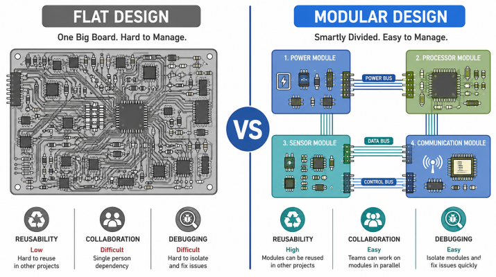
Every block has one job and a nice, tidy interface, and can be tested separately. The output is a project that grows as needed, encourages collaboration, and remains robust throughout revisions. In this guide, we will delve deeper into the meaning of modular design, compare it to flat design, and explore some best practices for making it effective. We will also explore how modular thinking is carried down to panelization, DFM, and manufacturing, and how a partner like JLCPCB can assist you in reliably turning multi-module boards into reality.
Understanding Modular PCB Design
What Modular PCB Design Really Means
So, what does modular PCB design really mean? It's the concept of breaking up a circuit board into functional blocks, each of which does a simple, well-defined job. A block can be a power supply stage, an RF front-end, the core of a microcontroller, or an interface to a sensor. Each module is designed, tested, and optimized individually and then stitched into the complete layout. It is in the same way you create with LEGO blocks rather than sculpt a statue from one stone.
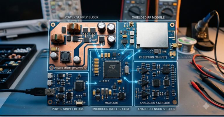
One brick is wrong; you change it, not the whole structure. In your EDA tool, this is typically made up of a hierarchical schematic. You no longer have one large sheet but multiple sub-sheets for each function, with links between them all on a master sheet that illustrates how the modules fit together. This reflects the real-life approach of engineers to system thinking, subsystem by subsystem. This is the same structure in the physical layout. The related components are clustered according to the function, the signal flow, and the power domain; your power section, digital core, and analog front end are all neatly contained in their respective areas of the copper.
Modular vs Flat Design: When to Choose Which
In flat design, all the components and net are located in a single schematic and layout, without any partitioning of functionality. If you're making a simple LED driver or a small breakout board, then this is fine and often faster. Modular design becomes appealing when complexity, re-use, and team size increase. Let's make a short comparison to help you make your decision:
| Factor | Flat Design | Modular Design |
|---|---|---|
| Complexity handled | Low to moderate | Moderate to very high |
| Schematic style | Single sheet | Hierarchical, multi-sheet |
| Reusability | Low, copy-paste prone | High, drop-in blocks |
| Team collaboration | Difficult, one file | Easy, parallel work |
| Debugging | Whole-board hunt | Isolated per module |
| Upfront effort | Minimal | Higher planning cost |
| Best for | Simple boards, quick prototypes | Complex, evolving, mixed-signal designs |
Opt for a flat design for smaller, singular boards where speed is more important than structure. Go with a modular design for complex projects, or ones that may change, or that are used by multiple people.
Major Benefits of Modular PCB Design
Improved Reusability, Maintainability, and Team Collaboration
It is the reusability that is the greatest benefit. Once validated, the same USB-C power delivery block can be reused in your next three projects, so no redesign is required. This kind of block reuse can lead to substantial decreases in development time on complex projects, as reported by industry practitioners. In parallel, maintainability is increased. If there is a failure that is determined to be the result of only one module, then that block, and not the entire board, is replaced or revised. This helps to reduce the extent of revisions and reduce long-term maintenance costs. Modular design really comes into its own with collaboration. As each module is on a separate sheet, several engineers may work simultaneously:
- One engineer is responsible for the power module, and another engineer is responsible for the communication interface.
- Analog and digital experts operate in isolation without infringing on each other's turf.
- Online PCB design is now possible to co-edit in real-time and track the versions in the cloud.
- Design reviews turn into conversations, rather than overwhelming marathons, on a block-by-block basis.
Faster Debugging, Easier Updates, and Reduced Errors
When a flat board has a problem, it's like looking for a needle in a haystack to find which solder joint is faulty. Modular design reduces the haystack. Each block is pre-validated on its own, and a fault typically ends up in one module, so you have a good idea of where to probe. Updates are easier, as well. Looking to upgrade your Wi-Fi module to BLE? When the interface pinout remains the same, you simply change the module and don't touch the rest of the board. This is the true idea behind scalability: adding or changing features without having to redesign. Less natural error ensues. Reusing tested blocks saves you from introducing new bugs – it's the same layout, footprint, and routing you've already tested. The more that a module is used, the more reliable it becomes.
Core Principles and Best Practices
Creating Effective Modules and Clear Interfaces
A good module has one job and a well-defined boundary. If you choose where those boundaries will be, partition by:
- Function: A separate group of power, communication, analog, and digital circuits.
- Signal flow: Group physically together blocks that have signals in common.
- Power domain: Group together power sections that share the same power rail.
- Physical limitations: Consider mounting points and mechanical areas.
- Complexity: Make each module small enough to be readable and testable.
The interface is the agreement among the modules. Describe all boundary-crossing signal names, communication protocols, power rails, and ground references. Connectors are standardized, like a common 2.54 mm pitch connector between mating boards, to ensure that modules are interchangeable. In high-speed nets, handle interfaces with care. Support controlled impedance (typically 50 ohm single-ended and 90-100 ohm differential) across module boundaries with no return path discontinuities, which cause signals to degrade at the boundary between two blocks.
Hierarchy Structure, Naming Conventions, and Version Control
Your map is a clean hierarchy. Your top-level schematic should be represented as a schematic of blocks with clearly labeled interconnects, with each sub-sheet containing the detail. The architecture should be understood in seconds by anyone who opens the project.
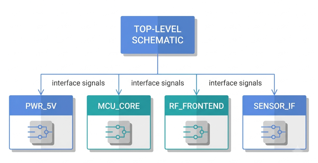
Naming conventions keep chaos bay. Use consistent names that are descriptive, like PWR_5V, MCU_CORE, RF_FRONTEND, and propagate these throughout the net labels, reference designators, and layout groups. Here, consistency will help you during each review and handoff. On projects where more than one engineer is involved, version control is a must. Make systematic changes, tracking, and have a tag for each block when they are validated for release. This is much easier than having to manage files like "final_v3_really_final" as many online PCB design tools have these features built in.
Design for Reusability and Scalability
For a module to be truly reusable, it should be an "independent" library element. Group its schematic, validated layout, and metadata describing its interface, constraints, and test conditions. Export to standard formats, such as Gerber and ODB++, for smooth transfer of the block from one tool to another or from one manufacturer to another. Scalability is to plan for growth from the outset. Allow headroom in interfaces, flexible pin assignments, and validate modules with realistic loads, ranging from a 2.4 GHz wireless interface to DDR memory timing. A block that has passed the stress test is a block you can rely on for your next and larger design.
From Modular Design to Manufacturing Success
Impact on Panelization, DFM, and Production Efficiency
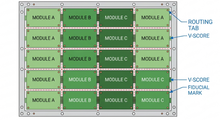
Panelization – arranging multiple board copies or multiple different modules on a single manufacturing panel. Modular design is a perfect fit for panelization as the individual blocks can be designed as separate boards on a panel, and then be de-panelized at a later time, for example, by V-scoring or tab routing. This translates to some tangible production gains:
- The repeated modules are panelized efficiently, reducing the material cost and the cost per module.
- Independent modules are available to assemble and test prior to final integration.
- Pick and place programming is simplified by consistent module footprints, which also help save setup time.
Design for Manufacturing – DFM – is also improved. If each module is designed to be trace space clean, annular ring minimum clean, and clearance clean, then the entire assembly is trace space clean, annular ring minimum clean, and clearance clean. DFM & DRC checks are performed per module, prior to final integration, to detect issues in their early stages when they can be resolved at the lowest possible cost.
Common Pitfalls and How to Avoid Them During Handover
Often, modular projects falter at the handover, when a design file moves from the designer to the fabricator. Be on the lookout for these pitfalls:
- Inconsistent interfaces: Mismatched pinout between mating modules. Early locking and/or documentation of interfaces.
- Panel spacing errors: When there is too little clearance for V-scoring or routing tabs, depaneling may break. Follow your fab's panel guidelines.
- Missing fiducials or tooling: With the modules being assembled separately, an alignment reference on the panel is still required.
- Incomplete file sets: Never send Gerbers, drill files, pick and place, or BOM without the others, and confirm to manufacturing standards.
JLCPCB's Expertise in Supporting Modular PCB Projects
Professional DFM Review Optimized for Modular Architectures

JLCPCB has an automated DFM review system, which can check clearance, annular ring, and spacing issues of the uploaded design before production. In the case of modular boards that comprise multiple individual blocks and have their own routing guidelines, this initial feedback can be used to ensure that each module is within the required fabrication tolerances. An instant quoting system also allows you to easily test stackup and spec options more quickly.
Advanced Manufacturing Capabilities for Complex Multi-Module Boards
In complex modular designs, a single board may combine a high-speed interface, a dense BGA module, and analog sections. JLCPCB offers multilayer stackups, controlled impedance, a variety of surface finishes, and even SMT assembly. An entire multi-module board can be fabricated and populated in one place. They allow for repeated or mixed modules to be efficiently panelized on a single panel with their panelization support.
Reliable Fabrication and Consistent Quality at Any Scale
From prototyping a single multi-module board to scaling up to production volumes, consistency is important. Fast turnaround, starting from a low entry price and established quality control, including AOI and electrical testing, repeatable results are crucial in modular projects, and JLCPCB can provide them. Looking to implement these principles? Their online PCB design workflow with EasyEDA integration makes it easy to go from a hierarchical schematic to a finished board.
FAQ about Modular PCB Design
Q: What is modular PCB design in simple terms?
It is the practice of splitting a complex board into smaller, self-contained functional blocks, such as power, communication, and sensing modules. Each block is designed and tested independently, then combined into the full board through clearly defined interfaces.
Q: What are the main benefits of modular PCB design?
The key benefits are reusability of proven blocks, easier maintenance, parallel team collaboration, and faster debugging because faults are isolated to individual modules. Together, these reduce development time, lower error rates, and make designs far more scalable.
Q: How does modular design affect panelization and manufacturing?
Independent modules map cleanly onto panelization, allowing multiple blocks or copies to share one panel and be separated by V-scoring or tab routing. This improves material utilization, simplifies assembly, and lets modules be tested before final integration.
Q: When should I use flat design instead of modular design?
Flat design is a good choice for small, simple boards or quick prototypes where structure adds little value and speed matters most. Once complexity, reuse, or team size grows, modular design becomes a more efficient and maintainable option.
Q: Which tools support hierarchical modular design?
Most modern EDA platforms, including EasyEDA, KiCad, and Altium Designer, support hierarchical schematics and reusable module libraries. Many online PCB design tools also add cloud version control and real-time co-editing, which makes collaborative modular work much easier.
Conclusion
Modular PCB design is more of a change of mindset: from making one huge board do everything, to creating a set of clean and reusable blocks that all perform a single task. That change affords you reusability, seamless collaboration, quicker debugging, and designs that grow with your ambitions rather than against them. Expand that to interfaces, naming, version control, and panelization, and complexity becomes manageable and not so scary.
Modular thinking will be even more important as electronics become increasingly dense and product lifecycles continue to shorten, particularly given the increasing influence of online PCB design platforms, which make hierarchical and collaborative working the norm. When it's time to step out of the structured schematic and into the real world of physical boards, DFM analysis, panelization support, and even integrated assembly services help to ensure that even the most demanding multi-module designs can be manufactured with confidence at JLCPCB.

Keep Learning
Is FR4 the Best Board Material for Your Design
Key Takeaways Best All-Rounder: Ideal balance of strength, insulation, and low cost for standard PCBs. Clear Limits: Poor heat dissipation (~0.3 W/m·K) and high loss for RF (>3 GHz). Alternatives: Use Rogers for RF, Aluminum for high heat, and FPC for flexibility. Selection Essentials: Pick High-Tg (170°C+) for lead-free reflow and custom stackups for impedance. JLCPCB Advantage: 1–32 layer FR4 boards with ±10% impedance control and 24h fast dispatch. In the world of electronics and printed circuit bo......
Optimizing High-Voltage Circuit Safety with PCB Dielectric Strength
Key Takeaways Non-linear Scaling: Dielectric strength drops as thickness increases. Safety vs Signals: Dielectric strength ensures safety, while Dk controls signal speed. Material Selection: High-voltage safety depends on Tg, CTI, and moisture resistance. Spacing Rules: Clearance prevents air arcs, while creepage prevents surface tracking. Assembly Testing: Hi-pot testing requires finished assemblies, not bare boards. Dielectric strength is the number engineers quote to prove a board is safe at mains ......
How Copper Foil Shapes PCB Performance and Manufacturing Quality
Key Takeaways Weight: 1 oz copper ≈ 35 µm thickness; higher weight increases current capacity. Types: ED for standard rigid boards, RA for dynamic flex circuits. DFM & Loss: Smoother foil lowers RF loss; thicker foil requires wider trace spacing. The part of a PCB that actually carries the electrical signal is the copper foil. The strength comes from the glass weave, the resin is used to keep the layers together, and the solder mask is used to provide protection and separation of exposed copper. But w......
A Complete Guide to Copper Clad Laminate (CCL) in PCB Manufacturing
Key Takeaways CCL is the base material: a cured resin-reinforcement sheet with copper foil bonded to one or both sides. Three parts control performance: Resin affects heat and loss, reinforcement controls stability, and copper foil affects conductor behavior. Choose by the main design stress: Heat, frequency, and cost usually determine the best laminate family. Slash sheets define the material: IPC-4101 uses numbered slash sheets to specify rigid PCB base materials. Tg alone is not enough: Td and time......
Buried Vias in Advanced PCBs: Enabling Higher Density, Better Signal Integrity, and Compact Designs
Key Takeaways Hidden Routing: Buried vias connect only inner layers, keeping outer surfaces clear for dense components and traces. Better Signal Integrity: They eliminate via stubs, reducing parasitics and signal loss in high-speed designs. Higher Density: Essential for HDI boards, dense BGAs, and small form factors like wearables. Higher Cost: Sequential lamination and extra drilling steps make them ~3×-4× more expensive than standard through-holes. Ever wondered how a modern smartphone mainboard can......
Unlocking Higher Density and Better Performance with Blind Vias in HDI PCBs
Key Takeaway Higher Density: Connects surface to inner layers without penetrating the whole board, freeing routing channels under fine-pitch BGAs. Improved Signal Integrity: Reduces via stub length to minimize impedance discontinuities in high-speed designs. Aspect Ratio Rule: Keep the depth-to-diameter ratio near 0.75:1 (max 1:1) for reliable laser drilling and void-free plating. Thermal Efficiency: Supports via-in-pad setups for better heat dissipation and compact component placement. Ever wonder ho......