
Hierarchical Design : Making Complex PCB Projects More Manageable
10 min
- Understanding Hierarchical Design in PCB Projects
- Major Benefits of Adopting Hierarchical Design
- Core Principles and Best Practices for Hierarchical Design
- Implementing Hierarchical Design from Schematic to Manufacturing
- JLCPCB's Expertise in Hierarchical Design Projects
- FAQ about Hierarchical Design
- Conclusion
Key Takeaway
Hierarchical design transforms complex PCB projects from overwhelming single-sheet nightmares into well-organized, modular, and manageable systems. By breaking down large schematics into functional blocks with clear interfaces, engineers can significantly improve organization, reduce errors, enhance reusability, and enable smoother collaboration. This approach not only simplifies debugging and layout but also leads to better DFM outcomes and faster time-to-market, making it the preferred methodology for modern, sophisticated PCB designs.
Ever been given a schematic with 300 components on a single page and been tempted to say, “Oh, that sucks”? Nets running all over, barely legible labels, and a power section wrapped up in high-speed signals. If this sounds familiar, Hierarchical Design is the methodology you've been looking for. The practice of creating a huge page to draw everything out just doesn't work anymore as boards become more complex. The modern products integrate processors, power management, RF front-ends, and dozens of interfaces on a single PCB.
Trying to perform all of that in one flat view is asking for mistakes, lost connections, and very lengthy debugging sessions. We will dissect the concepts and features of hierarchical design, its advantages, and the essential rules to adhere to. We'll also go through the process of taking a hierarchical project from schematic to manufacturing and how the fabricator JLCPCB fits in there.
Understanding Hierarchical Design in PCB Projects
What Hierarchical Design Is and How It Works
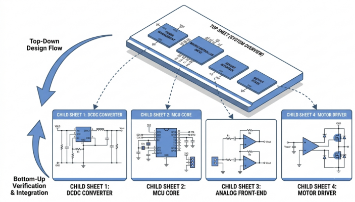
Hierarchical design is a way of organizing a schematic into “nested” modular blocks rather than a single schematic drawing. The top sheet is a sheet containing block symbols, each of which is a functional subcircuit like a power supply, the MCU core, or a sensor interface. Each block is connected to its own child sheet with the detailed circuit for that function. These levels can be navigated up and down as if they were chapters in a well-organized book and can be viewed as a set of modules. You don't have to manually copy nets; the EDA software takes care of the level-to-level connections.
There are two common ways to build this structure:
- Top-down: Designing at the top sheet, block symbols and their ports; filling the internal circuitry of blocks at the bottom.
- Bottom-up: Design the individual subcircuits first, then create block symbols based on them and add blocks to the top sheet.
Flat Design vs Hierarchical Design: Key Differences
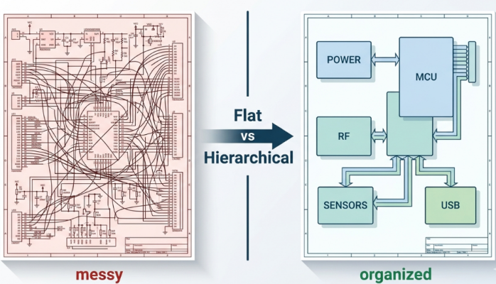
In a flat design, the entire circuit is on one sheet or a collection of loosely interconnected sheets, lacking any true parent/child relationships. For a 20- or 30-piece small board, that is OK. The problem begins to occur once the design is scaled. Flat schematics are frequently extensively duplicated and renamed by hand by engineers. When you make a typographical error in the net-name, you can get a duplicate net or an accidental short. The software does not enforce the links between sheets, and engineering changes require a manual scrub of each page. A summary of practical differences is given in the following table.
| Aspect | Flat Design | Hierarchical Design |
|---|---|---|
| Structure | Single or linear sheets | Nested blocks with child sheets |
| Scalability | Limited, gets messy fast | Handles large, complex projects |
| Reuse | Manual copy-paste | Reusable block modules |
| Error risk | Higher (manual net matching) | Lower (software-managed links) |
| Best for | Small, single-designer boards | Large, multi-engineer projects |
Major Benefits of Adopting Hierarchical Design
Better Organization, Reusability, and Team Collaboration
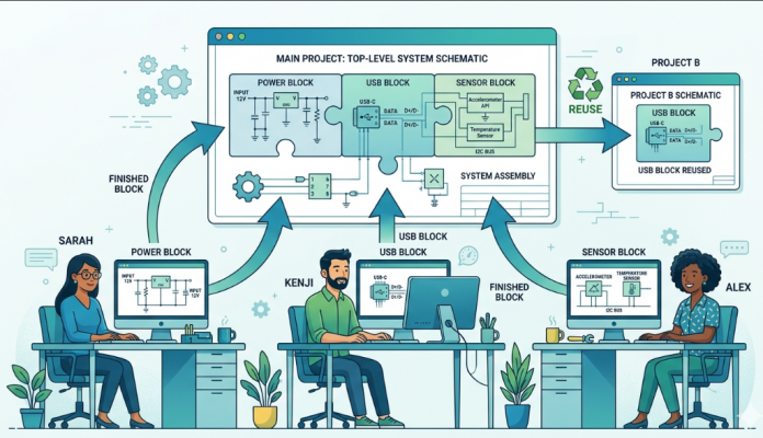
The initial advantage you experience is organization. You don't need to dig through a mass of nets, but a neat top sheet for each block that you can read to tell you what each part of the system does. This bird's-eye view makes reviewing quicker and onboarding new engineers much easier. Reusability is the next big win! When you have a power-supply block constructed and working (or a USB interface that has been tested), you can place the same module in your next project without having to redraw the diagram. The methodology states that you "reuse your circuits without the need to re-create [them], saving hours and preserving proven designs. A hierarchical design also creates true team collaboration:
- Multiple engineers may own different blocks concurrently.
- The interface of each block is clearly designated, and integration is predictable.
- Once a module is validated, it is a trusted building block for an entire team.
- Design reviews may be targeted to a single functional area at a time.
Improved Error Reduction and Easier Debugging
Manual repetition is the enemy of errors, and flat schematics are rife with it. Each duplicated circuit and each retyped net label is an opportunity for a short circuit or a broken connection, as well. With a hierarchical design, that danger can be reduced as the software handles the connection between standard blocks. Debugging is also made simple. A power rail that is misbehaving, you open the power block and inspect a contained, well-defined circuit rather than tracing nets across a whole flat page. The fault is contained within a module, and you waste less time searching and more time fixing. There is also a quality benefit on the standards level. Cleaner, modular schematics make clearances and sizing of conductors easier to check against IPC-2221 or other guidelines, since each function block can be checked against the guidelines before integration.
Core Principles and Best Practices for Hierarchical Design
Creating Effective Modules and Proper Hierarchy Levels
The first step for good modularization is to think in terms of functions. Each block should be a full function, with a defined purpose, and very little interaction with the other blocks. Strive for high cohesion within the block, and a minimal number of signals crossing the block boundary. Below are some practical guidelines for defining modules and levels:
- Divide by function, NOT by page count: Don't split circuits into parts that don't belong together, such as one half of a regulator stage.
- Keep interfaces narrow: The fewer ports a block exposes, the easier it will be to reuse and verify it.
- Limit hierarchy depth: Typically, two or three levels are enough, as anything more can make it tedious.
- Make blocks self-contained: The block should be meaningful and, preferably, self-simulating.
- Standardize repeated structures: When using 4 identical channels, create one block and clone it many times.
Maintaining Connectivity, Naming Conventions, and Version Control
Hierarchical designs are successful or unsuccessful with connectivity. Note that nets are local within a block; thus, all connections from the outside must go through a correctly named port with the same name as its parent-sheet pin. The most common hierarchical bug is using a different port name. There must be a real discipline for naming conventions:
- Name the ports consistently and descriptively, like VBUS, SDA_MCU, or CLK_50M.
- Only use global labels for true global nets, such as power and ground.
- Do not use generic names such as NET1, which convey no intent and invite mistakes.
Implementing Hierarchical Design from Schematic to Manufacturing
Transitioning Smoothly to PCB Layout and Routing
Your schematic can help you plan your physical layout. Many EDA (electronic design automation) programs have room or block-based placement, which allows you to place all components in one schematic block in the same location on the board. It's a modular placement that does have a number of benefits:
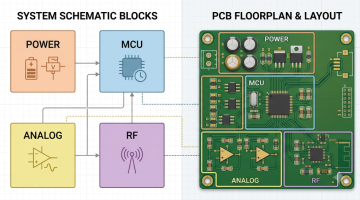
- Functional sections remain physically small, reducing critical traces.
- Noise-producing switching blocks can be separated from sensitive analog or RF blocks.
- The close proximity of related signals and their references ensures that paths return clean.
- One module can be routed at a time, making it easier to achieve high-speed length matching and impedance control.
How Hierarchical Design Supports Better DFM Outcomes
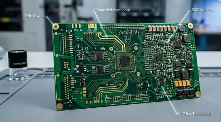
Modular and well-documented design makes design for manufacturing (DFM) a lot easier. Every block validated has its known footprints, clearances, and component selections to minimize the risk of an unexpected rule violation at the fabricator. Since modules are reusable and tested, common DFM problems such as acid traps, inadequate annular rings, or tight solder-mask slivers typically get caught once and are fixed forever in the source block. This fix is then copied to all instances of the block's use. Faster turnaround with a cleaner and consistent Gerber and pick and place output, fewer back-and-forth queries when submitted for fabrication.
JLCPCB's Expertise in Hierarchical Design Projects
Strong Support for Complex Multi-Level Schematics
With EasyEDA's seamless integration, JLCPCB provides a user-friendly journey from design idea to production, especially for those who work with hierarchical designs. Create schematics with multiple sheets, break them up into blocks, and get an instant quote for push-to-manufacture. Well-structured schematic to order flow is important, particularly on larger projects, where it's a time saver to export clean Gerbers and BOMs from a well-structured design. This workflow maintains the entire process, from the initial symbol to the final order, for modular boards that are created with reusable components.
Reliable Production for Sophisticated PCB Systems
Hierarchical design is most used on precisely the type of high-level boards that require regular, repeatable manufacturing. With the help of JLCPCB's automated lines and inspection processes such as AOI and electrical testing, every time you reuse a module, you can be certain it is manufactured to the same standard. Then throw in SMT assembly that includes component sourcing, and you can go from a clean schematic to an assembled and tested multi-block design. For teams working on large projects, that's the end-to-end reliability that makes good hierarchical design into reliable hardware.
FAQ about Hierarchical Design
Q: What is hierarchical design in PCB schematics?
Hierarchical design organizes a schematic into nested, modular blocks instead of one large flat sheet. A top sheet holds block symbols, and each block links to a child sheet with its detailed circuitry, while the EDA software manages connections between levels.
Q: When should I use hierarchical design instead of flat design?
Use flat design for small, single-designer boards with only a few dozen parts. Switch to hierarchical design when projects grow large, involve multiple engineers, or require reusing proven subcircuits across designs.
Q: How do connections work between hierarchical blocks?
Nets inside a block are local and only connect outward through named ports that match the parent-sheet pins exactly. Global signals such as VCC and GND are the exception and connect automatically throughout the design.
Q: Does hierarchical design help with PCB layout and manufacturing?
Yes. Block-based structure enables modular placement and cleaner routing, keeping functional sections compact. It also improves DFM outcomes because validated, reusable modules carry proven footprints and clearances, reducing the risk of repeated errors.
Conclusion
Hierarchical design has become an essential methodology for tackling today’s increasingly complex PCB projects. By transforming sprawling flat schematics into clean, modular, and reusable functional blocks, it delivers superior organization, dramatically reduces errors, and accelerates both development and manufacturing processes. Whether you are a solo designer or part of a large engineering team, adopting hierarchical principles will help you build more reliable boards with greater confidence and efficiency. As PCB systems continue to grow in density and functionality, embracing hierarchical design is no longer optional — it is the smartest way forward. Start applying these practices in your next project and experience the difference in clarity, speed, and quality with JLCPCB’s seamless design-to-production workflow.
Popular Articles
Keep Learning
The Comprehensive Guide to Circuit Symbols: Key to Understanding Electrical and Electronic Diagrams
Note Need a quick reference while reading schematics? Download our free, printable Circuit Symbols Cheat Sheet (PDF), featuring the most common IEC and ANSI symbols organized by category. Keep it on your desktop or print it for easy reference at your workbench. ⬇ Download the Free Circuit Symbols Cheat Sheet (PDF) Every electronic diagram is written in a visual language, and circuit symbols are its alphabet. From your first electrical schematic to a multi-layer board, knowing circuit symbols can make ......
Hierarchical Design : Making Complex PCB Projects More Manageable
Key Takeaway Hierarchical design transforms complex PCB projects from overwhelming single-sheet nightmares into well-organized, modular, and manageable systems. By breaking down large schematics into functional blocks with clear interfaces, engineers can significantly improve organization, reduce errors, enhance reusability, and enable smoother collaboration. This approach not only simplifies debugging and layout but also leads to better DFM outcomes and faster time-to-market, making it the preferred ......
Why a Clean PCB Netlist Is the Foundation of Successful Manufacturing
Key Takeaways A clean PCB netlist is the foundation of successful manufacturing, serving as the single source of truth that bridges schematic and physical PCB layout. By ensuring accurate component data, net connections, and version control, it prevents costly errors, improves yield, and enables reliable production. Mastering IPC-D-356 netlist best practices helps engineers reduce risks and achieve high-quality results with JLCPCB. Ever wonder what exactly the link is between your wonderfully drawn sc......
PCB Board Design: A Step-by-Step Guide for Beginners
Key Takeaways This PCB Design Guide offers beginners a practical step-by-step approach to designing a compact 3A IP2312 lithium battery charger PCB — an upgraded alternative to the popular TP4056 module. It focuses on key techniques like schematic creation, optimized layout, proper trace routing for 3A current, and ground planes to build efficient and reliable boards. Printed Circuit Boards (PCBs) form the backbone of most modern electronic devices, providing a platform to connect electronic component......
PCB Silkscreen: All You Need to Know
Key Takeaways The PCB Silkscreen Guide demonstrates that a properly designed legend layer is essential to prevent assembly failures and ensure long-term hardware reliability. By mastering modern manufacturing methodologies like Direct Legend Printing (DLP) and aligning layouts with JLCPCB's strict DFM design rules—including the absolute 0.8 mm character height limit and the automated 0.15 mm silkscreen clipping protocol driven by solder mask precedence—engineers can seamlessly eliminate cold joints an......
Choosing the Best PCB Color-Enhancing Aesthetics and Functionality
Key Takeaways Choosing the best PCB solder mask color involves balancing aesthetics, visibility, and functionality. Green remains the top choice for superior contrast and inspection, while black offers premium appeal, white excels in LED applications, and other colors like purple and red provide unique design options. The ideal color depends on your priorities in inspection ease, thermal performance, and brand image, with minimal impact on electrical performance when using proper silkscreen contrast. ......