JLCPCB Officially Launches HDI PCB Manufacturing Services
Product Update
Sep 14, 2026- Enabling More Compact, High-Performance Designs
- JLCPCB HDI Manufacturing Capabilities
- Versatile Application Fields
- Experience It Today
JLCPCB has officially launched its HDI PCB manufacturing services, expanding its PCB manufacturing capabilities to meet the growing demand for high-density, miniaturized, and high-performance electronic designs.The HDI option is now available on the JLCPCB online quotation page , allowing users to select it as needed.
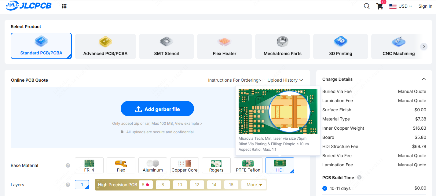
As a core building block of modern electronic products, HDI PCBs drive rapid innovation across consumer electronics, automotive electronics, 5G communications, and IoT fields through their ultra-high routing density, miniaturized design, and exceptional electrical performance.
Enabling More Compact, High-Performance Designs
With growing demand for high-frequency, high-speed transmission, HDI boards have become a key solution for compact and high-performance electronic designs. The newly launched HDI service delivers several core advantages:
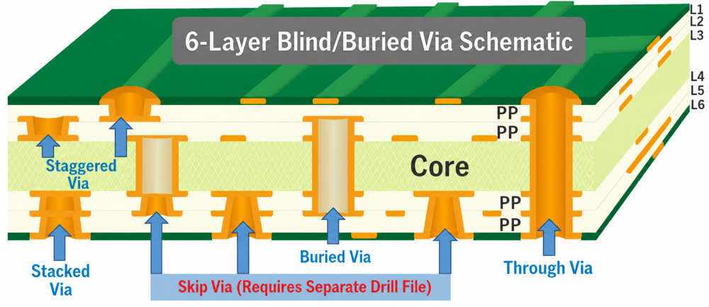
- Optimized Routing: Smaller line widths, tighter spacing, compact pads, and microvias improve design efficiency and spatial utilization.
- Compact Design: Smaller dimensions and footprints support space-constrained designs and advanced packaging applications.
- Multilayer Interconnection: Supports high standards for electrical performance and efficiency.
- Premium Materials & High Reliability: JLCPCB uses Shengyi and Nanya laminates, combined with advanced production processes to support reliable and stable HDI PCB manufacturing.
JLCPCB HDI Manufacturing Capabilities
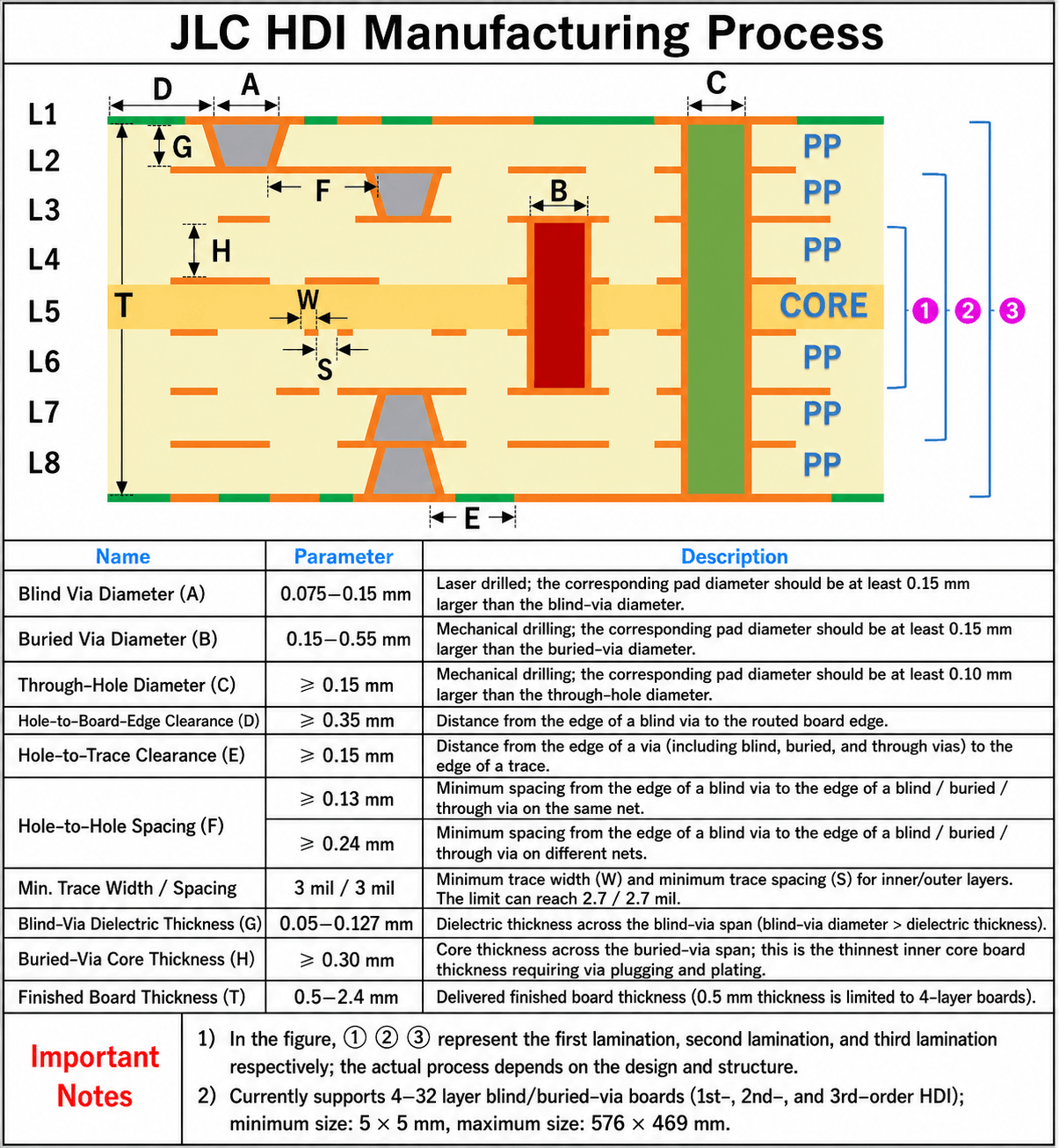
Leveraging advanced smart manufacturing, JLCPCB offers competitive manufacturing specifications with tight process control for HDI production. Global customers can refer to the following diagram for precision control of manufacturing processes and spatial layouts:
Versatile Application Fields
Whether powering high-integration consumer electronics or high-reliability applications, the new HDI boards support a wide range of electronic products:
- Smart Terminals: Smartphones, tablets, digital cameras, and high-integration portable devices.
- High-Reliability Applications: Automotive electronics, aerospace, and advanced medical equipment.
- Communication & Networking: 5G communication equipment, high-end routers, and network gear.
Experience It Today
The new HDI PCB ordering options are now officially live on the digital platform. Engineers and business customers worldwide can now upload their Gerber files to experience faster, cost-effective, and premium-quality high-density interconnect manufacturing, accelerating the journey from concept to market.