
Optimizing Return Paths in PCBs: Strategies for Minimal Noise and Maximum Integrity in High-Speed Designs
12 min
- Core Elements That Shape Effective Return Paths
- Proven Techniques to Strengthen Return Paths
- Manufacturing Precision Required for Robust Return Paths
- JLCPCB’s Expertise in Building Flawless Return Path PCBs
- Frequently Asked Questions (FAQ)
Here is a fundamental truth that every PCB designer should have tattooed on their forearm (figuratively, of course): every signal current requires a return current. Unless you take time to provide it with a low-impedance path, the current will simply seek whatever it can, and you are going to end up having some very undesirable hotspots. The entire concept of a current loop is the reason why the return is so difficult. In essence, when the signal passes between point A and point B, you now have a loop: the signal travels in one direction, and the return travels in the opposite direction between point B and point A - usually through the ground plane or whichever reference plane you are working with.
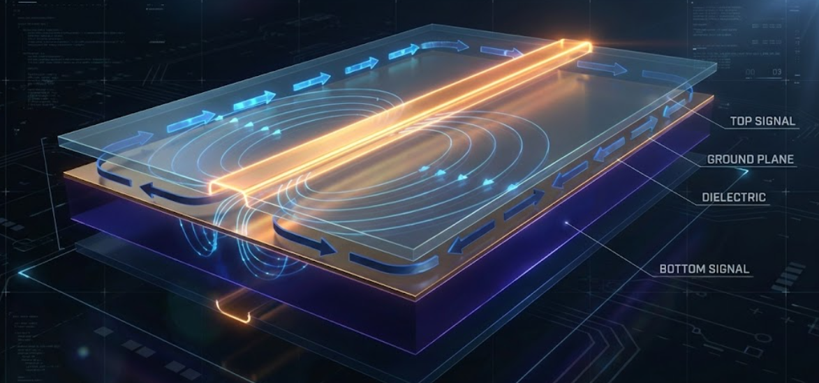
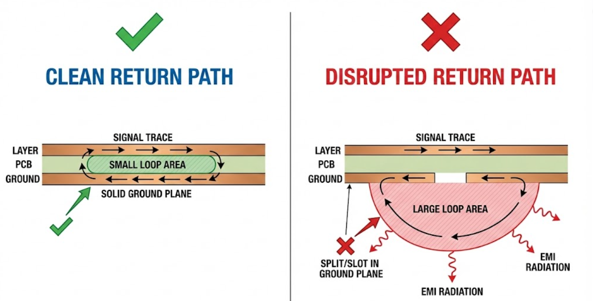
The loop area determines the inductance, the extent to which the signal is affected, as well as the amount of EM radiation that it produces. You get low inductance, practically zero radiation, and high noise immunity with a tight, small loop, think signal trace right over an undamaged ground. A large, wandering loop, when the return path is broken or split up, will result in high inductance, more radiation, and a signal that is noisier. And that is more or less the difference between a clean and a crappy design, even in the way you manage your return paths.
Common Issues from Disrupted Return Paths in Modern Boards
Disrupted return paths manifest as a variety of symptoms that can be maddeningly difficult to diagnose if you do not understand the underlying cause. Ground bounce occurs when return currents from multiple signals share a common, inductively limited path, creating voltage fluctuations on the ground reference that appear as noise on every signal. Crosstalk is aggravated when the return currents of a given signal are compelled to share a path with the return currents of adjacent signals. EMI spikes occur when the currents on the returns are forced to go around plane splits, slots, or voids, adding area to the loop and transforming the loop into an efficient antenna.
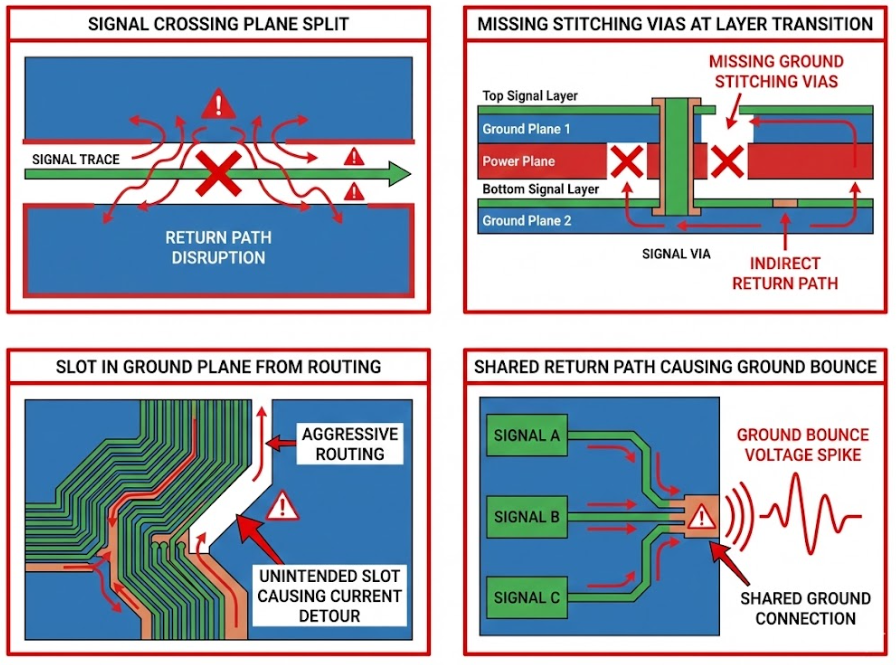
The most frequent design errors that cause return-path problems are routing signals across ground-plane separations without a nearby return path bridge, via transitions with changes in reference plane without stitching vias to allow return currents to interact, anti-pad removal of ground-plane copper, thermal reliefs, or routing, and mixing signal and power on the same reference without consideration of the interaction between return currents.
Core Elements That Shape Effective Return Paths
Role of Continuous Reference Planes and Ground Planes
The most important thing is the ground plane, which is the most significant when it comes to clean return paths. The low-impedance return path is the one that is provided by a solid, continuous, unbroken reference plane adjacent to each signal layer. In DC and low frequencies, the return current simply diffuses all over the entire plane, but above about 100 kHz, the current begins to concentrate directly under the trace in a narrow band, and it is traveling the path of least impedance (not resistance). This frequency-dependent behaviour implies that any puncture in the ground plane immediately below a high-frequency trace causes the return current to be rerouted, and a very narrow slot, such as one that a trace on the ground layer makes, or an otherwise quite hostile thermal relief pattern, can be a significant source of trouble to very fast signals.
Simply put, to have those fast signals acting, you actually need to have the ground plane intact in the area directly under the high-frequency traces. Even a little notch or slot may misdirect the flow of returning current and may cause trouble, and it is better to eliminate it or to ensure that the plane of the ground is continuous. The reference plane does not have to be grounded; it can be a power plane, as long as it provides a continuous, low-impedance AC return path. Decoupling capacitors between the power plane and ground ensure that the power plane is AC-grounded at the frequencies of interest.
Via Fence and Stitching Vias for Path Continuity
Stitching vias are ground vias placed at regular intervals along the board or around specific areas to connect ground planes on different layers, ensuring return current continuity throughout the stackup. Without adequate stitching, ground planes on different layers may develop voltage differentials at high frequencies, degrading return path quality. A via fence is a row of closely spaced ground vias that creates a conductive wall between circuit sections. Via fences serve dual purposes: they provide return path continuity for signals transitioning between layers, and they create electromagnetic isolation between adjacent circuit zones. The via spacing should be less than one-tenth of a wavelength at the highest frequency of concern to maintain effective shielding.
Strategic placement near signal layer transitions is particularly important. When a signal moves from one layer to another through a via, its return current must also transition between reference planes. Placing ground stitching vias immediately adjacent to the signal via provides a low-inductance path for this return current transition. Without these stitching vias, the return current must find an alternate path, increasing loop area and radiation.
Pro-Tip: Place at least two ground stitching vias within 50 mils of every signal via that changes reference planes. This single practice eliminates more return path problems than any other design technique.
Managing Plane Splits and Layer Transitions
Plane splits are sometimes necessary separate analog and digital ground regions, isolated power domains, or mixed-signal board partitioning may require breaks in the ground plane. The critical rule is: never route a high-speed signal across a plane split without providing a return current bridge. Return current bridges can take several forms. A row of stitching capacitors (100nF to 1nF, depending on frequency) placed across the split near the signal crossing provides an AC return path.
A narrow copper connection between the split regions at the crossing point works for lower frequencies. Or, if possible, route the signal on a layer that uses a different, continuous reference plane that does not have the split. Layer transitions present similar challenges. When a signal moves from a layer referenced to one plane to a layer referenced to a different plane, the return current must also transition. The stitching vias between the two reference planes at the transition point serve as the return current bridge.
Proven Techniques to Strengthen Return Paths
Minimizing Loop Area Through Optimal Routing
The general idea of return path optimization is to make the area of each of the existing loops as small as possible on the board. Some of the practical techniques that I have found useful are: routing signals on the adjacent layers as close to their reference planes as possible to reduce the vertical portion of the loop area, making traces as short and straight as possible to reduce the horizontal portion, ensuring that the layers are not adjacent to a discontinuous reference plane, and clustering similar signals together such that the currents of the returns flow on the same part of the reference plane.
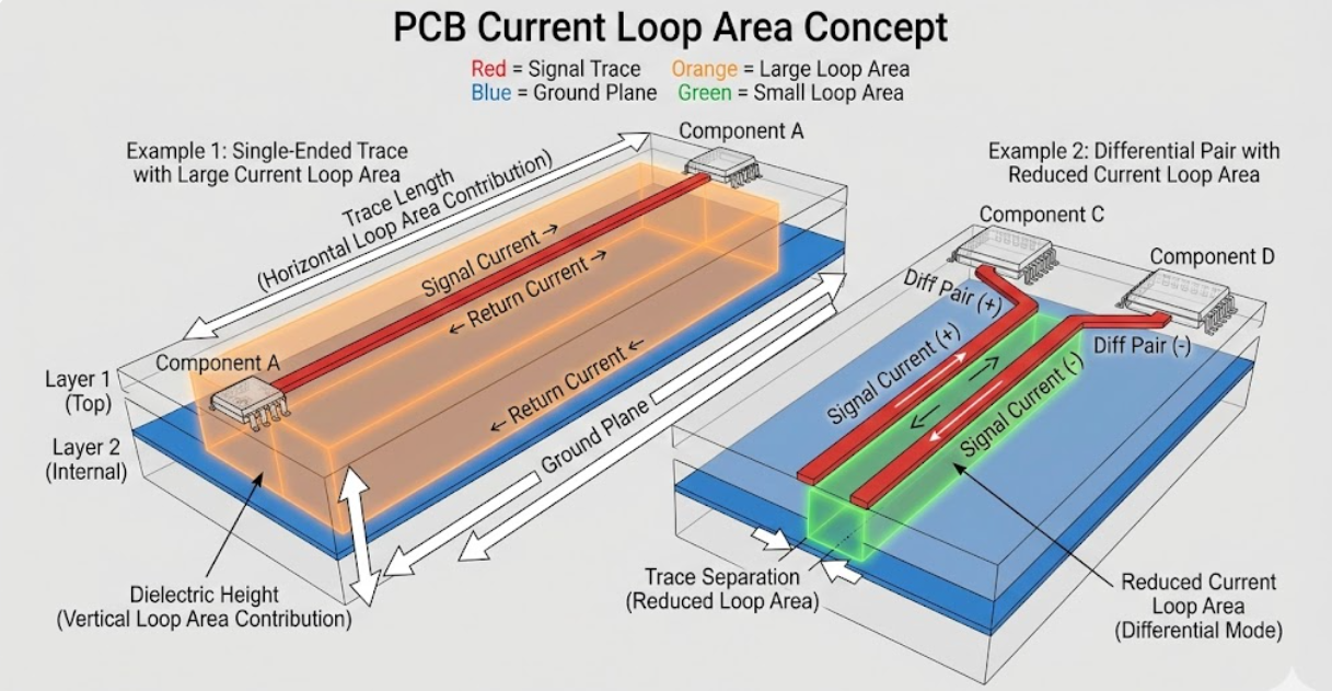
In the case of differential pairs, the return current in every trace passes halfway through the other trace and halfway through the reference plane. When you hold the pair tight, the trace-to-trace return current is much larger, which causes the loop area to naturally contract in comparison with the reference plane.
Strategic Via Placement for Low-Inductance Returns
Every via transition is an opportunity to create or prevent a return path problem. The key practice is straightforward: whenever a signal via changes layers, place ground vias immediately adjacent to provide a low-inductance return current path between the reference planes. For single-ended signals, two ground vias flanking the signal via (one on each side) provide excellent return path continuity. For differential pairs, ground vias between and beside the pair vias create a quasi-coaxial transition structure.
For high-speed signals above 5 GHz, four or more ground vias surrounding the signal via may be warranted to control the via transition impedance. The via inductance decreases with decreasing via length and increasing via diameter. For critical return path vias, use the largest practical hole size and shortest possible via length (blind vias are preferred over through-hole vias for this reason).
Integrating Decoupling and Guard Traces
Decoupling capacitors serve a dual role: they provide local charge storage for power delivery, and they create AC bridges between power and ground planes, ensuring that power planes can serve as effective return path references. Place decoupling capacitors close to active components and distributed across the board to maintain low impedance between power and ground at all frequencies of interest.
Guard traces are grounded copper traces placed between sensitive signals and potential aggressors, providing additional isolation by intercepting coupling fields and shunting them to the reference plane through stitching vias. Guard traces are most effective when they are stitched to the ground plane at regular intervals (every 500 mils or less) along their length.
Manufacturing Precision Required for Robust Return Paths
Ensuring Plane Integrity Through Accurate Lamination and Etching
Return path quality depends on manufacturing precision. Ground plane continuity requires accurate etching that does not create unintended thin spots or breaks in the copper. Lamination quality determines the dielectric thickness between signal traces and reference planes, which affects return current distribution and impedance.
Layer-to-layer registration accuracy ensures that ground planes are properly positioned relative to signal traces. A misregistered ground plane effectively changes the impedance environment for overlying signal traces and can create unexpected return path discontinuities near board edges, where registration errors are typically largest.
Controlled Via Drilling and Plating for Reliable Connections
Vias and return-path vias must remain solid and low-resistance in order to keep the ground planes attached throughout the time the board is operating. It implies that we must keep our drills very clean, round, no burrs, no tear-out, we must apply enough copper plating in the via barrel (typically 20-25µm minimum), we must ensure that the pad feeds into the barrel correctly at each level the via penetrates.
When we want a high-quality reliability project, one of the most important choices would be the IPC Class 2 or Class 3 fab standard; it will ensure the quality of the via is reliable in the long term. Cross-section a couple of sample vias, and you can triple-check that the plating thickness and finish are in check.
Advanced Inspection to Verify Path Continuity
Our electrical tests (flying probe or bed-of-nails) are to ensure that the ground planes and stitching vias have actually been connected. The micro-section run checks the integrity of the barrel and the quality of plating. In high-speed work, we will go so far as to pull TDRs on specific test patterns to observe the behavior of the impedance across critical signal paths, which indirectly informs us that the quality of the return-path is as we wanted it to be.
Automated Optical Inspection (AOI) identifies copper defects on the ground plane layers, which might cause unwanted slots or breaks. Combining all these inspection steps, we are sure that the finished board will provide the return-path integrity that we invested in the layout.
JLCPCB’s Expertise in Building Flawless Return Path PCBs
High-Precision Multi-Layer Fabrication for Unbroken Planes
JLCPCB’s multi-layer fabrication capabilities deliver the precision required for uncompromised ground plane integrity. Tight layer registration, controlled etching, and consistent lamination ensure that every ground plane is continuous, properly positioned, and precisely spaced from adjacent signal layers, which are the foundation of excellent return path performance.
Specialized Support for Via Stitching and Fence Implementations
Designs with dense via stitching patterns and via fences demand drilling accuracy and plating consistency across hundreds or thousands of additional vias. JLCPCB’s automated drilling systems handle these via-dense designs with the positional accuracy and throughput needed for both prototype and production volumes.
Consistent Quality Delivering Superior Signal Integrity

The cumulative effect of precise fabrication, accurate registration, clean etching, consistent plating, and verified connectivity is a board that delivers the signal integrity performance designed into the layout. JLCPCB’s quality systems ensure this consistency across every board in every order, giving designers confidence that their return path strategies will perform as intended.

Frequently Asked Questions (FAQ)
Q. What is a return path, and why does it matter?
A return path is the route that the current takes to complete the circuit from the signal’s destination back to its source. It matters because the quality of the return path directly affects signal integrity, noise, EMI radiation, and crosstalk. A disrupted return path is one of the most common causes of noise and EMC problems in PCB designs.
Q. How do stitching vias improve return path performance?
Stitching vias connects ground planes on different layers, providing low-impedance paths for return currents to transition between layers. They ensure that the return current can follow the signal as it moves between layers and prevent voltage differentials between ground planes that would degrade signal quality.
Q. Can I route signals across a ground plane split?
It is strongly discouraged for high-speed signals. If unavoidable, provide a return current bridge (stitching capacitors or a narrow copper connection) across the split immediately adjacent to the signal crossing. Better yet, route the signal on a different layer that has an unbroken reference plane.
Q. How many ground vias should I place near each signal via?
At a minimum, place two ground vias near each signal via that changes reference planes. For high-speed signals (above 1 Gbps), three to four ground vias surrounding the signal via are recommended.
Q. Does the via fence spacing matter?
Yes. Via fence spacing should be less than one-tenth of the wavelength at the highest frequency of concern for effective electromagnetic isolation. At 3 GHz, this means a pacing of about 10mm or less. At 10 GHz, spacing should be 3mm or less. Tighter spacing provides better isolation at higher frequencies.
Keep Learning
The Critical Role of Copper Peel Strength in Durable PCB Performance
Key Takeaways Standard Test: Measured via the IPC-TM-650 90° pull test in N/mm. Core Function: Prevents pad lifting and delamination under thermal stress and CTE mismatch. Foil Types: ED foil provides higher adhesion; RA foil yields lower signal loss. Material Benchmarks: Standard FR4 averages 1.0–1.4 N/mm, while High-Tg FR4 achieves 1.2–1.6 N/mm. Design Tips: Add teardrops, eliminate unsupported copper slivers, and perform DFM checks. Ever wonder what's making the copper stay put on your circuit boar......
How Modular PCB Design Simplifies Complex Electronics Projects
Key Takeaway Modular PCB design simplifies complex electronics by breaking boards into independent, reusable functional blocks with clear interfaces. It boosts reusability, speeds up debugging, enhances team collaboration, and reduces errors.Shift from flat to modular design for faster development and more scalable, reliable PCBs. Ever seen a 400+ component schematic and got your head scrambled before even beginning routing? You are not alone. With the ever-increasing density of electronics combined w......
Your Ultimate Guide to PCB Rulers
In the world of PCB design and manufacturing, having the right tools is crucial for achieving accuracy and precision. One such tool that has gained popularity among professionals and hobbyists is the PCB ruler. This specialized measuring tool is designed to provide accurate measurements, reference information, and component footprints, assisting designers, engineers, technicians, and assemblers in various stages of PCB development. In this guide, we'll explore what a PCB ruler is, the features and mea......
Understanding the Materials Used in PCBs: Selection, Types, and Importance
Key Takeaways FR-4 is the go-to material for most cost-effective and reliable PCBs. Use Rogers for high-frequency and RF applications to reduce signal loss. Higher copper weight (2oz) improves current and heat handling. Choose High-Tg substrates for better thermal stability in multilayer boards. Green LPI soldermask offers the best balance of performance and inspection. Printed circuit boards (PCBs) are an essential component of modern electronics. These boards connect and support electronic component......
How to Select Tg of PCB ?
What is the Tg of PCB? In PCB manufacturing, "Tg" stands for Glass Transition Temperature. It is the temperature at which the PCB substrate material transitions from a rigid, glassy state to a soft, rubbery state. PCBs are flame-retardant (UL94 V-0) and do not burn easily; instead, they soften above Tg. The Critical Correlation Between Tg and Z-Axis CTE (Coefficient of Thermal Expansion) When the temperature exceeds the Tg point, the PCB substrate material (such as standard FR-4) undergoes a physical ......
How to Choose the Thickness of PCB
First, In the world of electronic products, the PCB is often referred to as the "heart" of the device. It interconnects all components, making board thickness one of the most important parameters. Choosing the right PCB thickness directly affects the electrical performance, mechanical stability, thermal management, and long-term reliability of the final electronic product. The process of selecting PCB thickness is influenced by various factors, such as product application scenarios, board material, an......