
Annular Rings in PCB Design: Mastering Reliable Via Connections and Precision Fabrication
12 min
- Beyond the Basic Formula: What Actually Determines Your Ring Width
- IPC-6012 Annular Ring Requirements: What the Spec Actually Says
- Tolerance Stack Analysis: Where Your Ring Budget Goes
- Routing Density vs. Ring Integrity: The BGA Trade-Off
- Teardrops: The Free Reliability Upgrade You Should Always Use
- Manufacturing Realities: Drilling, Plating, and Inspection
- DFM Integration: Catching Problems Before Production
- JLCPCB’s Precision Approach to Annular Ring Fabrication
- Conclusion
- Frequently Asked Questions (FAQ)
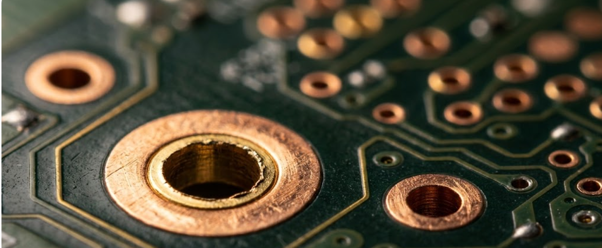
In fact, I have a question, which is worth considering: when did you last actually compute the worst-case annular ring size of your PCB, including all fabrication tolerances? When you say, or not recently, you are certainly not the only ones. We simply scale pad sizes to the EDA defaults or what we have already used without further checking whether this number measures up to the actual drill wander, layer mis-registration, and etch compensation. The only mechanical and electrical connection between the plated via barrel and the copper pads on each of the layers is that thin ring of copper around all the holes that have been drilled.
Nobody notices it at all when it is just sufficient. With it being marginal, you will have intermittent failures that will remain and plague production engineers months later. Today, we are going to go beyond the textbook definition. We will deconstruct the tolerance stack, which in fact sets your actual annular-ring margin, take a careful look at the IPC-6012 class requirements (and give them their due), and also go through design techniques that trade off routing density versus manufacturing robustness.
Beyond the Basic Formula: What Actually Determines Your Ring Width
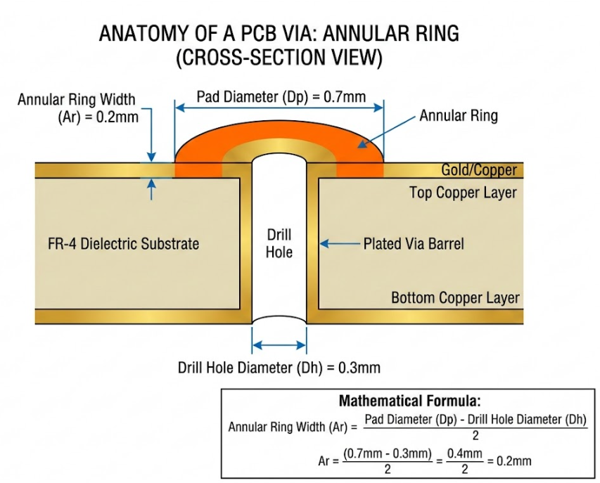
You can work it out yourself: the width of the annular rings is half the difference between the pad diameter and the diameter of the drill. A pad 0.7mm deep and 0.3mm drilled is thus, on any side, 0.2mm, or about 8mils, deep. The thing is, that such a little calculation is more of a nominal number, not the one you will have after the entire manufacturing chain. The actual annular ring is actually the nominal value minus the total of all the tolerances that accrue in the process.
The ring does two jobs at once. Electrically, it is the area of contact of the electroplated barrel with the pad copper on each layer; it directly influences the via resistance and the actual amount of current that can pass through it. Mechanically, it clamps the via in place on the laminate, and it pulls against pad lift when the thermal drill is applied, and the copper and FR-4 have different expansion rates, straining the barrel-to-pad contact.
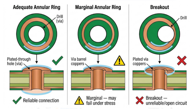
The problems will manifest themselves when the ring is only marginally sufficient. The via can pass electrical, reflow, and appear okay a few weeks later, only to begin experiencing intermittent opens after a few thermal cycles. This is because the small copper connection begins to erode over time. These types of defects that are hidden but follow IPC 6012 are the very defects that the stricter specs are designed to prevent in Class 3 situations.
IPC-6012 Annular Ring Requirements: What the Spec Actually Says
IPC-6012 defines minimum annular ring requirements across three product classes, but the numbers alone do not tell the full story.
| Parameter | Class 1 (General) | Class 2 (Dedicated Service) | Class 3 (High Reliability) |
| Minimum Annular Ring (External) | 0.050mm (2 mils) | 0.050mm (2 mils) | 0.050mm (2 mils) |
| Minimum Annular Ring (Internal) | 0.050mm (2 mils) | 0.050mm (2 mils) | 0.050mm (2 mils) |
| Breakout Permitted (External) | Yes, 90 degrees | Yes, 90 degrees | No breakout |
| Breakout Permitted (Internal) | Yes, 180 degrees | Yes, 90 degrees | No breakout |
The critical distinction is not the minimum width itself, which is identical across classes, but the breakout allowance. Class 1 and Class 2 permit partial breakout as long as the minimum ring width is maintained on the remaining arc. Class 3 permits zero breakout on any layer, meaning the drill must land entirely within the pad boundary everywhere on the board.
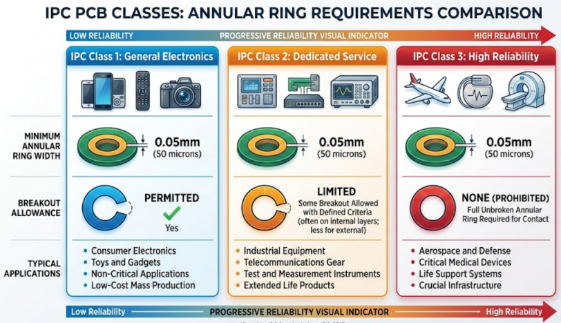
This zero-breakout requirement is what drives pad sizes significantly larger in high-reliability designs. You are not just designing for nominal placement; you are guaranteeing that even with maximum tolerance accumulation, no drill hole touches a pad edge on any layer.
Tolerance Stack Analysis: Where Your Ring Budget Goes
This is where the rubber meets the road. Your nominal annular ring gets consumed by a stack of fabrication tolerances.
The Key Contributors
- Drill positional accuracy: Standard CNC drilling achieves +/-0.075mm (3 mils). Premium equipment can hit +/-0.025mm (1 mil).
- Inner layer registration to tooling: Typically +/-0.050mm (2 mils), driven by imaging accuracy and material dimensional stability.
- Lamination registration shift: Heat and pressure can shift inner layers by +/-0.025 to 0.075mm.
- Etch compensation variation: The variation in lateral etch contributes +/-0.013 to 0.025mm.
- Drill-to-lamination registration: X-ray targeting alignment adds +/-0.025 to 0.050mm.
For a worst-case RSS (root sum square) analysis on a standard 4-layer board, the combined tolerance can reach 0.10 to 0.15mm. Your 0.20mm nominal ring could shrink to 0.05 to 0.10mm on the worst via in the panel.
Practical Design Targets
Given this reality, here are annular ring targets that actually work in production.
| Application | Target Ring (Outer) | Target Ring (Inner) | Rationale |
| Consumer (Class 2) | 0.150mm (6 mils) | 0.175mm (7 mils) | Standard tolerance margin |
| Industrial (Class 2) | 0.175mm (7 mils) | 0.200mm (8 mils) | Extended life margin |
| Automotive/Medical (Class 3) | 0.200mm (8 mils) | 0.250mm (10 mils) | Zero breakout budget |
| Mil/Aero (Class 3) | 0.250mm (10 mils) | 0.300mm (12 mils) | Maximum reliability margin |
Inner layers need larger targets because they accumulate more tolerance contributors through the lamination and registration chain.
Routing Density vs. Ring Integrity: The BGA Trade-Off
Consider a 0.8mm-pitch BGA. With a 0.3mm drill and a 0.125mm annular ring target, you need a 0.55mm pad. The gap between adjacent pad edges is just 0.25mm. Depending on the trace/space capability, that may allow one trace at 4/4 mil rules or none at 5/5 mil.
Dropping to a 0.1mm ring with a 0.50mm pad opens the gap to 0.30mm, potentially allowing an extra trace. But you have traded manufacturing margin for routing freedom. Can your fabricator hold tight enough tolerances to make that 0.1mm ring reliable?
For 0.5mm and 0.4mm-pitch BGAs, microvias become a necessity. Laser-drilled microvias achieve positional accuracy of +/-0.013mm (0.5 mil), dramatically tightening the tolerance stack. A 0.250mm pad with a 0.100mm laser drill gives a 0.075mm annular ring that, after the tighter tolerance budget, is actually more reliable than a mechanically drilled via with a nominally larger ring.
When to push smaller rings: your fabricator confirms tighter registration, you are using laser-drilled microvias, or the application is Class 2 with breakout allowed. When to back off: near board edges, around mounting holes, for high-current vias, or any Class 3 design.
Teardrops: The Free Reliability Upgrade You Should Always Use
Teardrops are small copper fillets at the trace-to-pad junction that create a smooth geometric transition instead of an abrupt width change. They reduce stress concentration at the interface during thermal cycling and effectively increase the annular ring in the direction of the approaching trace.
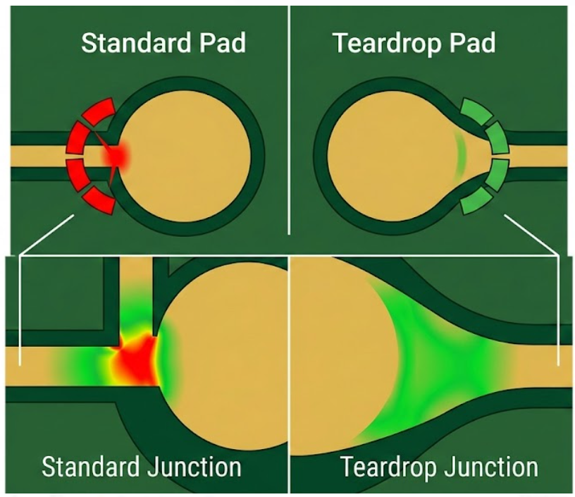
If drill wander shifts the hole toward the incoming trace, the teardrop provides extra copper that would not exist with a standard circular pad. Most EDA tools, including KiCad, Altium, and EasyEDA, apply teardrops as a batch operation after routing. The process adds negligible file size, zero manufacturing cost, and measurable thermal cycling improvement. There is genuinely no reason to skip them. Combine teardrops with copper pour connections to pads for maximum mechanical support. A pad tied to a large pour resists lifting far better than an isolated pad on a single trace.
Manufacturing Realities: Drilling, Plating, and Inspection
Drilling: The Dominant Variable
Drill positional accuracy is the single largest contributor to annular ring variation. Beyond machine capability, several real-world factors add error.
- Drill bit run-out increases with spindle wear, adding positional error beyond axis accuracy.
- Material movement during drilling, especially on thin or large panels, shifts hole positions relative to copper patterns.
- Stack height in multi-panel drilling introduces more error in the lower panels from drill deflection.
Modern fabricators like JLCPCB use high-speed CNC systems with automated tool management and SPC monitoring to minimize these variables. But designers should understand that quoted positional accuracy represents process capability, not a per-hole guarantee.
Plating: Completing the Connection
The annular ring only functions if barrel plating makes intimate contact with the pad copper on every layer. The critical process chain runs from clean drilling (no smear or tear-out), through desmear processing (permanganate or plasma), to electroless copper seeding, and finally electrolytic plating to specification thickness (20-25 micrometers for Class 2, 25 micrometers minimum for Class 3).
Inadequate desmear is particularly insidious. A thin resin film between barrel plating and the inner layer pad copper creates a high-resistance interface invisible to AOI that may only show up as resistance drift during field operation.
Inspection and Verification
Fabricators verify annular ring compliance through complementary methods: AOI on outer layers, X-ray for inner layer alignment, cross-sectional microsectioning of test coupons (the IPC-6012 gold standard), and electrical testing for functional verification. JLCPCB combines automated DFM checks at order submission with in-process AOI, electrical testing, and coupon-based microsection analysis to ensure compliance from design through final inspection.
DFM Integration: Catching Problems Before Production
The most cost-effective place to solve an annular ring problem is in the design phase. When DFM flags marginal rings, you have four options ranked by preference.
- Increase pad diameter if routing space permits. Simplest and most reliable fix.
- Decrease drill diameter if the via requirements allow a smaller finished hole. Dropping from 0.3mm to 0.25mm adds 0.025mm per side.
- Switch to microvias for problematic vias. Laser drilling's tighter tolerance effectively increases your ring budget without changing pad sizes.
- Request tighter registration from your fabricator, usually at additional cost. Last resort because it shifts the burden to manufacturing.
JLCPCB's online DFM system evaluates annular ring compliance automatically when you upload design files, flagging marginal vias at standard process tolerances. This pre-production check gives you the opportunity to adjust before committing to fabrication.
JLCPCB’s Precision Approach to Annular Ring Fabrication
Advanced Drilling and Alignment Technologies
JLCPCB’s CNC drilling systems deliver the positional accuracy needed for reliable annular rings across all board classes. High-precision spindles, automated tool management, and real-time depth control ensure clean, accurately placed holes that maximize annular ring quality. Combined with tight inner-layer registration control during lamination, these capabilities support robust via connections even at aggressive pad sizes.
Strict Tolerance Controls for High-Reliability Outputs
For boards requiring IPC Class 2 or Class 3 compliance, JLCPCB applies strict tolerance controls throughout the fabrication process. Layer registration is verified against the specification before drilling. Drill accuracy is monitored through statistical process control. And finished boards undergo a comprehensive inspection to verify that annular ring quality meets the required standard at every via location.
Comprehensive Support Ensuring Flawless Via Structures
JLCPCB’s DFM system automatically evaluates annular ring compliance when you upload your design files, flagging any vias that may have marginal rings at the fabricator’s standard tolerances. This early warning gives you the opportunity to adjust your design before committing to production, preventing yield issues and ensuring reliable via connections in every board delivered.
Conclusion

Annular ring design sits at the intersection of electrical reliability, mechanical integrity, and manufacturing reality. The nominal calculation is trivial, but designing rings that survive the full tolerance stack across every via on every layer requires disciplined analysis and practical experience.
The key takeaway: your annular ring target should be driven by your fabricator's actual tolerance capability, not by IPC minimums alone. Those minimums define acceptance criteria for finished boards, not design targets that ensure you get there reliably. Combine adequate ring sizing with teardrops, proper DFM analysis, and an understanding of where your tolerance budget goes, and you eliminate one of the most common sources of PCB field failures.
If you are ready to put these principles into practice, JLCPCB's combination of tight drilling registration, automated DFM analysis, and multi-stage inspection makes it straightforward to achieve reliable annular rings across all board classes. Upload your design files to get instant DFM feedback and start production with confidence that your via connections will perform exactly as designed.

Frequently Asked Questions (FAQ)
Q. What is an annular ring in PCB design?
An annular ring is the copper pad area surrounding a drilled hole in a PCB. Its width is calculated as (pad diameter minus hole diameter) divided by two. It provides the mechanical and electrical connection between the plated via barrel and the copper traces on each layer.
Q. What is the minimum annular ring width I should design for?
For commercial products (IPC Class 2), design for a minimum annular ring of 0.15mm (6 mils) on outer layers to provide adequate manufacturing margin. For high-reliability applications (IPC Class 3), target 0.2mm (8 mils) or more.
Q. What causes annular ring breakout?
Breakout occurs when the drilled hole is offset from the pad center far enough that the drill extends beyond the pad boundary on one or more sides. Causes include drill positional error, inner layer registration error during lamination, and material movement during processing.
Q. Do teardrops really improve reliability?
Yes. Tear drops reduce mechanical stress at the trace-to-pad junction and effectively increase the annular ring in the trace direction. Studies show measurable improvement in thermal cycling reliability with tear drops.
Q. How does JLCPCB verify annular ring quality?
JLCPCB uses automated DFM checks during order processing, AOI on fabricated panels, electrical testing for connectivity verification, and cross-sectional analysis on sample coupons. This multi-layered quality approach ensures annular ring compliance from design validation through final inspection.
Popular Articles
Keep Learning
How to Design Your Own Keyboard PCB: From Layout to Firmware
Designing a custom keyboard PCB is one of the most rewarding entry points into practical electronics. You not only get a really useful product on your desk, but also you learn schematic capture, matrix scanning, footprint selection, USB, and firmware. Most of the hardware engineers use the same skills that show up on professional boards. This guide walks the entire build from choosing switches, wiring the diode matrix, adding the microcontroller and USB-C, laying out the board, and flashing QMK or VIA......
Don't Let Design Errors Ruin Your Hardware: The Complete Guide to PCB Design Verification
Key Takeaways PCB design verification is the systematic process of validating layouts against electrical, signal integrity, and manufacturing rules before production, preventing costly board respins and launch delays. Schematic verification through Electrical Rules Check (ERC) catches floating inputs, power shorts, and footprint mismatches before layout begins. Design Rule Checking (DRC) ensures trace widths, clearances, and via sizes comply with your fabricator's manufacturing tolerances, especially ......
How to Determine the Right PCB Voltage Clearance for Safe and Reliable Designs
Key Takeaways Clearance is the air gap; Creepage is the surface path — both essential for high-voltage safety. Base spacing on peak voltage and follow IPC-2221 / IEC 60664-1 standards. Major factors: voltage, pollution degree, CTI, altitude, and conductor location. Use isolation slots, guard rings, and conformal coating to optimize spacing. Always run clearance calculations, DFM checks, and Hipot testing before production. Why do two copper traces that work fine at 5V suddenly arc over and burn at 400......
Mastering PCB Footprints: Design Best Practices for Reliable Manufacturing
Key Takeaways A PCB footprint (land pattern) translates component datasheet dimensions into copper pads, solder mask openings, paste apertures, silkscreen, and clearance areas that enable reliable soldering and assembly. Follow IPC-7351 standards and manufacturer DFM rules for pad dimensions, spacing, and layer design to minimize defects like solder bridging, tombstoning, and cracked joints. Choose between through-hole (THT) and surface mount (SMT) footprints based on electrical needs, thermal perform......
How Copper Thieving Balances Your PCB for Better Manufacturing Results
Key Takeaways Copper thieving adds non-functional copper patterns (dots, squares, or crosshatch) to balance copper density across PCB layers. This effectively reduces uneven plating (from 20-30% to <10%), board warpage, inconsistent etching, and impedance issues, delivering tighter tolerances, better solder mask adhesion, higher yields, and lower costs. For best results, target 40-60% copper density per layer, maintain proper clearances, and ensure stackup symmetry. When done right, it transforms comp......
ZIF Connectors Simplify Flexible PCB Assembly with Tool-Free Reliability
Did you ever attempt to mate a fragile flex cable into a connector and experience that unpleasant resistance, and wonder whether you were tearing off the tail or breaking the casing? It is precisely that tension that the ZIF connectors were supposed to help remove. Zero insertion force technology allows you to slide a flexible printed circuit or flat flexible cable into the receptacle to be mated with, using almost no push force at all, but rather allows a mechanical actuator to hold the cable firmly ......