
Via in Pad (VIP) Technology : Driving Density and Reliability in Advanced PCB Fabrication
11 min
- When and Why to Use Via in Pad Plated Over (VIPPO)
- Design Best Practices for Successful Via in Pad Implementation
- Precision Manufacturing of Via in Pad Structures
- How JLCPCB Masters Via in Pad
- Frequently Asked Questions (FAQ)
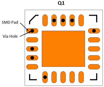
Via in pad is exactly what it sounds like: placing a via directly within a component’s soldering pad rather than routing it off to the side with a short trace. While this concept seems straightforward, it represents a significant evolution in PCB design philosophy that has become essential for modern high-density interconnect (HDI) boards.
In traditional PCB design, vias were always placed outside the component pad area, connected by a short fanout trace. This approach works fine when you have plenty of real estate. But as component packages have shrunk, think BGA pitches dropping from 1.27mm to 0.4mm and below. There simply is not enough room between pads to route escape traces to external vias. The PCB via in pad technique solves this by eliminating the fanout entirely, placing the via directly in the pad, and recovering precious routing space.
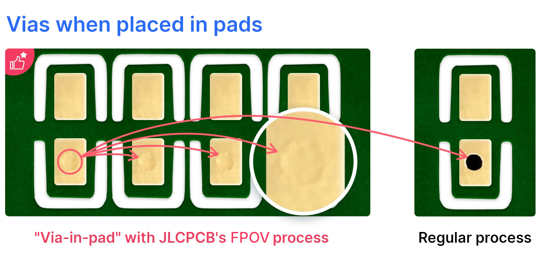
The evolution of via in pad technology closely mirrors the advancement of HDI manufacturing capabilities. Early implementations were limited to simple through-hole vias in pads (often causing solder wicking issues), while modern in-pad via solutions use filled and capped microvias that present a perfectly flat, solderable surface to the component above.
Core Advantages for Space Savings and Signal Performance
The benefits of via in pad extend well beyond simple space savings, though that alone would justify its popularity.
1) Routing density improves dramatically. By placing vias directly under BGA balls, you can escape signals from inner rows without consuming valuable surface routing channels. A 0.5mm-pitch BGA that would require four or more routing layers with traditional fanout might need only two layers with via in pad, potentially reducing your stackup and overall board cost.
2) Signal integrity gets a significant boost as well. Shorter signal paths mean reduced parasitic inductance and capacitance. For high-speed designs, eliminating the fanout stub removes a potential impedance discontinuity that can cause reflections and degrade signal quality. The pad-in via approach provides the shortest possible electrical path between the component and inner layers.
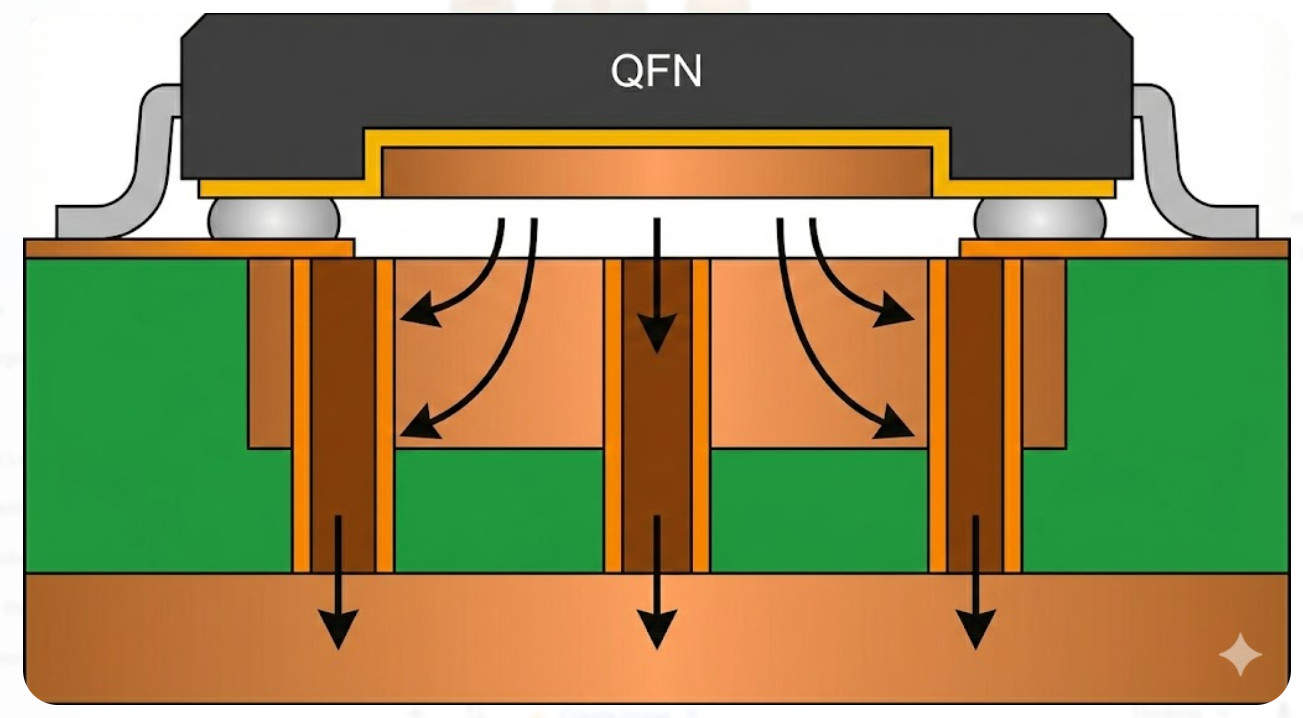
3) Thermal performance also improves. Filled vias in thermal pads create direct copper connections to internal ground or power planes, dramatically improving heat dissipation from power components and high-current ICs. This is particularly valuable for automotive and power electronics applications.
When and Why to Use Via in Pad Plated Over (VIPPO)
Ideal Scenarios in BGA, Fine-Pitch, and Thermal-Critical Applications
Via in pad plated over (VIPPO) is the gold standard implementation of via in pad technology. The process involves drilling the via, filling it with conductive or non-conductive material, plating copper over the fill, and planarizing the surface to create a smooth, flat pad. This ensures that the component sits on a surface indistinguishable from a solid pad.
The ideal scenarios for VIPPO include BGA escape routing where pitch is 0.8mm or finer, and inner-row signals cannot escape through traditional dog-bone fanout. It is also essential for QFN and DFN packages with exposed thermal pads, where filled vias provide critical thermal pathways to internal planes. High-frequency applications above 3 GHz benefit from the eliminated stub effect, and any design where board real estate is at an absolute premium will benefit from the density improvement.
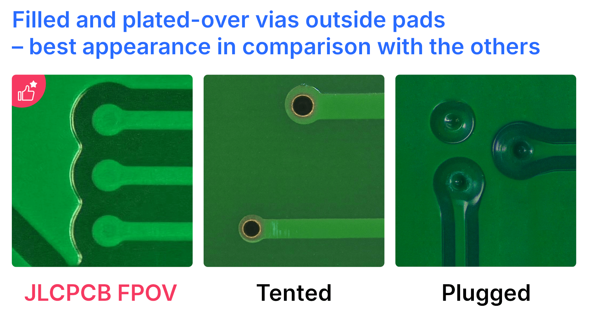
Pro-Tip: Not every via in pad needs to be VIPPO. For prototype runs or less critical applications, tented or plugged vias in pads may suffice. Reserve full VIPPO for fine-pitch BGAs and thermal-critical pads where planarity is non-negotiable.
Comparison with Traditional Via Placement Strategies
Traditional via placement uses a “dog-bone” pattern: a short trace routes from the component pad to a via placed in the clearance between pads. This approach is simple, well-understood, and does not require any special manufacturing processes. However, it consumes routing space, adds trace length (increasing inductance), and becomes physically impossible at very fine pitches.
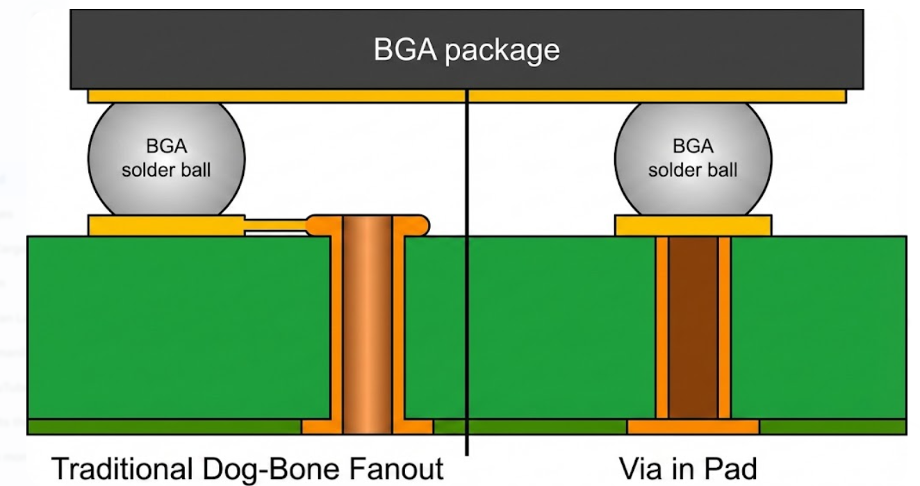
Via in pad eliminates these compromises but adds manufacturing complexity and cost. The filling, plating, and planarization steps are additional process stages that require specialized equipment. The trade-off is straightforward: if your design can accommodate traditional fanout without routing congestion or signal integrity issues, save the money and use dog-bones. If you are pushing density limits or chasing every last dB of signal margin, via in pad is worth the investment.
Design Best Practices for Successful Via in Pad Implementation
Pad Size, Hole Diameter, and Filling Material Guidelines
Via generation in a pad begins essentially in a schematic and layout tool. Microvias (laser-drilled) Pad applications Pad hole diameters (commonly 0.25 -0.35 mm) and pad diameters (commonly 0.25 mm). Typical hole diameter ranges from 0.075 to 0.15 mm. In microvias, Pad application, Pad hole diameters 0.25 -0.35 mm, Pad diameters 0.25 mm -0.35 mm
The fill material is a matter of choice, depending on the job. Copper paste or electroplated copper conductive fills are the most conductive in terms of thermal and electrical, and are thus used as thermal vias beneath power pads. Light and less expensive, non-conductive fills epoxy-based) It can be used in signal vias where thermal conductivity is not as important. Both of these still require to be copper-plated and leveled. The most important rule: ensure that your pad is large enough to support the via hole, the annular ring, as well as to allow sufficient solder paste to cover the component. A via occupying excessive pad area will reduce the solder joint reliability.
Stackup Planning and Impedance Control Integration
Via in pad designs interact directly with your stackup. Microvias used in pad applications typically span only one or two layers, which means your stackup must place the target routing layer adjacent to the component layer. HDI stackups with sequential lamination (1+N+1 or 2+N+2 configurations) are designed specifically to accommodate this requirement.
Impedance control becomes more nuanced with a via in the pad. The via itself introduces a small capacitive discontinuity in the signal path. For designs above 10 Gbps, 3D electromagnetic simulation of the via structure may be warranted to ensure the impedance profile meets your budget. At moderate speeds, the discontinuity is typically negligible compared to the improvement gained by eliminating the fanout stub.
DFM Rules to Avoid Common Pitfalls
Common via-in-pad design mistakes include using via holes that are too large for the pad (violating minimum annular ring requirements), failing to specify filled and capped vias in the fabrication notes, placing vias in pads without accounting for the soldermask opening adjustment, and neglecting to verify that the fab house can actually achieve the required via-to-pad registration tolerance.
Always communicate your via-in-pad requirements clearly in your fabrication drawing. Specify fill type (conductive vs. non-conductive), cap plating requirements, planarity tolerance, and whether a dimple is acceptable on the opposite side. Ambiguity in your fab notes leads to assumptions by the manufacturer, and assumptions lead to problems.
Pro-Tip: Include a cross-section drawing in your fab notes showing exactly how you expect the via in pad to be constructed. A picture truly is worth a thousand words when communicating with your fabricator.
Precision Manufacturing of Via in Pad Structures
Laser Drilling, Conductive Filling, and Planarization Processes
When you are designing these in-pad structures, then it is a precision multi-step process. In the case of the microvias, we drill blind holes with UV or CO 2 laser, which is insane in terms of accuracy - typically locking in±25 um. You must tune the laser settings to the right or you will make a mess of a hole that will destroy the pad of the capture layer.
Once the drill is done, you stuff the via with one of a few choices. The most popular one is a screen-print with either conductive or non-conductive paste, particularly blind microvias. Electrolytic copper filling is also gaining momentum lately due to its superior conductivity and reliability. After filling up the via, then you polish the surface with a ceramic or diamond abrasive wheel to ensure that the cap is level with the rest of the copper. Lastly, you plate a copper cap on the filled via, making it fuse with the pad. The final product is an object that appears and behaves like a solid pad, which is electrically and mechanically.
Copper Plating and Void-Free Filling Techniques
The large problem in the manufacture of via-in-pad structures is the elimination of voids. Any confined air or gas bubbles may burst out during reflow soldering and form solder balls, blow holes, and flaky joints, and consume the thermal conductivity of the vias. The current fabbers employ vacuum-assisted fill, rheology of paste, and multi-pass screen printing to ensure that there are few voids. They also operate X-ray scans and cross-sectional cuts to verify the quality of the fill. In fact, electro-lytic copper filling discards fewer voids than the paste ones, so it is becoming the choice of high-reliability applications.
Advanced Inspection for Reliability Assurance
Checking via-in-pad quality exceeds the standard PCB sweep. X-rays show concealed cavities, unfinished fillings, and registration mistakes that are beyond the naked eye. We then perform micro-sectioning of sample coupons to check fill quality, cap thickness, and general structure.
Planarity is checked using profilometry or optical inspection to ensure that the via cap is flat enough, typically not more than 1 0 -mil or 0.2 mm dimple or bump of the pad. All these checks ensure that all the via-in-pad will withstand assembly as well as the entire life of the product.
How JLCPCB Masters Via in Pad
State-of-the-Art Equipment for Microvia and Filling Precision
JLCPCB’s production lines feature advanced UV and CO2 laser drilling systems capable of producing microvias as small as 0.075mm in diameter with industry-leading positional accuracy. Combined with automated via filling and precision planarization equipment, these capabilities enable reliable via in pad structures across a wide range of board designs.
Integrated Capabilities from Prototyping to Volume Production
Whether it is a handful of prototype boards that you are just trying to make sure that BGA escape routing works, or you are getting ready to make fifty thousand production panels each month, we maintain the same tight process controls on every order. The transition of prototype to volume is so seamless that the tested design just transfers directly to mass production, devoid of any ugly process re-qualification surprises that would otherwise put a wrench in your schedule.
Proven Expertise in Delivering High-Yield, Reliable VIP PCBs

We have done thousands of assignments via-in-pad, smartphones, telecommunications equipment, automobiles, and the industry. The depth of experience here is that the engineering staff has already addressed and overcome nearly all of the via-in-pad challenges you may encounter, be it ultra-fine-pitch BGA escape or high-current thermal via arrays. All you need to do is upload your design files and have the DFM system raise any possible snags before the production process begins.

Frequently Asked Questions (FAQ)
Q. What exactly is via in pad, and why would I need it?
Via in pad places a via directly within a component’s soldering pad instead of routing to an external via. You need it when the component pitch is too fine for traditional fanout, when you need maximum routing density.
Q. Does via in pad plated over (VIPPO) cost more than standard vias?
Yes. VIPPO requires additional manufacturing steps, including via filling, planarization, and cap plating. The cost premium varies by fabricator but typically adds 15-30% to the bare board price. The trade-off is justified when design density or signal performance requirements demand it.
Q. Can I use via in pad with through-hole vias, or only microvias?
Both are possible, but microvias (blind vias spanning one or two layers) are preferred for via in pad applications. Through-hole vias are harder to fill completely and tend to create larger solder wicking channels. If through-hole vias in pads are necessary, specify plugged and capped vias in your fabrication notes.
Q. What happens if vias in pads are not properly filled?
Unfilled or partially filled vias in pads can cause solder wicking during reflow, where solder flows down through the via instead of forming a proper joint on the pad. This leads to insufficient solder joints, intermittent connections, and long-term reliability failures. Always specify fill requirements clearly.
Q. How small can via in pad structures be fabricated?
Modern laser drilling can create microvias as small as 0.05mm in diameter for advanced HDI applications. Practical via in pad implementations at JLCPCB typically use 0.1mm to 0.15mm diameter microvias with corresponding pad sizes of 0.25mm to 0.35mm.
Keep Learning
Enhancing PCB Reliability: A Deep Dive into VIA-in-PAD Design
Key Takeaways Space Saving: VIA-in-PAD (POFV) places vias directly inside SMD pads, maximizing routing channels and board miniaturization. Flawless Soldering: Epoxy filling and copper capping eliminate the risk of solder siphoning, ensuring flat, perfectly solderable pads. Maximum Performance: Direct vertical paths under components drastically lower thermal resistance and eliminate high-speed parasitic inductance. JLCPCB DFM Targets: Maintain mechanical via hole diameters between 0.25 mm and 0.35 mm, ......
How Stacked Vias Enable Higher Density and Better Performance in HDI PCBs
Key Takeaways Stacked vias are a critical technology that enables higher routing density and superior performance in HDI PCBs. By vertically aligning microvias in a single column, often combined with via-in-pad designs, they dramatically reduce breakout area, shorten signal paths, lower parasitic inductance, and improve thermal conductivity compared to traditional staggered vias. While requiring precise sequential lamination, via filling, and strict design rules, stacked vias help designers reduce lay......
Via in Pad (VIP) Technology : Driving Density and Reliability in Advanced PCB Fabrication
Via in pad is exactly what it sounds like: placing a via directly within a component’s soldering pad rather than routing it off to the side with a short trace. While this concept seems straightforward, it represents a significant evolution in PCB design philosophy that has become essential for modern high-density interconnect (HDI) boards. In traditional PCB design, vias were always placed outside the component pad area, connected by a short fanout trace. This approach works fine when you have plenty ......
Understanding Multilayer PCB Design in Modern Electronics
Introduction As electronics changes quickly, people want devices that are smaller and more powerful. This has led to the development of more advanced printed circuit board (PCB) designs. Multilayer PCBs are very important for meeting these needs because they offer higher density, when better usefulness in a smaller package. The complicated PCBs are used in a lot of high-performance devices, like smartphones, telecommunications gear, medical devices, and industrial machines. This article covers with a ......
Comparing High-Density PCB Stack-Up With Normal PCB
High-density printed circuit boards (PCBs)are not the same as simple PCBs. Do you know what the difference is? PCBs with a larger number of layers and a higher density of traces are known as HDIs. These are not as common because they are not used in small prototypes or hobby work, but for more professional application. One of the best examples of an HDI board with a complex stack-up that you can see—or might have—is the motherboard of your PC. HDI changes the story completely when it comes into the pi......
High-Density Interconnect (HDI): Revolutionizing PCB Design for Modern Electronics
In the world of advanced electronics, High-Density Interconnect (HDI) technology has become a game-changer. As devices get smaller, faster, and more complex, traditional printed circuit boards (PCBs) often face limitations in handling these demands. That’s where HDI PCBs come into play. This article covers what HDI is, why it’s critical, and how it’s shaping the future of modern electronics. 1. What is High-Density Interconnect (HDI)? A "HDI" printed circuit board (PCB) is one type whose wire count pe......