Choosing Rigid PCBs for High-Density and Cost-Effective Hardware Designs
16 min
- Defining the Fundamentals of Rigid Circuit Boards
- Essential Features and Design Benefits of Rigid PCBs
- Architectural Comparison: Rigid vs Flexible PCBs
- Why JLCPCB is the Leading Global Choice for Precision Rigid PCB Fabrication
- FAQ about Rigid PCB
- Conclusion
Key Takeaways
- Structural Stiffness: Doubling rigid PCB thickness makes it eight times stiffer.
- FR-4 Function: Glass fibers provide strength; epoxy resin governs thermal expansion.
- Crack Prevention: Place ceramic caps 5 mm from score lines to stop flexing damage.
- Cost & Use: Rigid boards cost less and carry heavy parts; use flex only for bending.
- Factory Tolerances: Design for 10% thickness variation and 20% trace width changes.
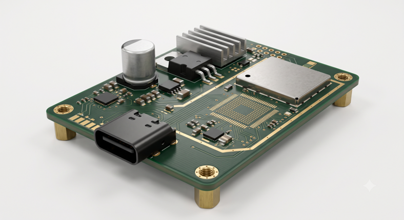
Rigid PCBs are more than just a place to attach parts. They become part of the product's structure, carry signals, remain flat, survive assembly, and withstand the mechanical stresses of the daily use of the end product during the anticipated life of the finished hardware. The performance of that structural job depends on the material stackup. FR-4, glass weave, resin content, copper thickness, and construction determine stiffness, dimensional stability, and fabrication cost. These choices are most important when considering a rigid board versus a flexible PCB for the same product envelope.
In this guide, you will learn:
- What a rigid PCB is, and what actually makes it stiff
- How FR-4 glass weave and resin content set the thickness and strength
- The features that keep a board flat through reflow and service
- Where rigid boards beat flexible ones, and where they lose
- Real material, panel, and assembly numbers for rigid vs flexible PCB
- What to check in a fabricator's tolerance list before you order
Defining the Fundamentals of Rigid Circuit Boards
Imagine a bridge deck that does not move when cars are on it. A rigid PCB operates similarly – the substrate protects traces, pads, and connectors. A flexible circuit conforms to the enclosure rather than carrying heavy pieces of hardware.
What is Rigid PCB and How It Differs in Mechanical Architecture
A rigid PCB is made with a hard material that is designed to stay flat during use. The factory etches copper onto a glass-reinforced epoxy panel, ensuring that all traces, pads, components, and connectors remain in the same position for the entire product's working life.
Stiffness is a function of material and thickness, and the stiffness increases with thickness cubed. Doubling the thickness from 0.8mm (31mil) to 1.6mm (63mil) will make it 8 times as difficult to bend the board. Proceeding to 2.0 mm (79 mil) will double the stiffness again.
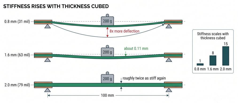
Example: A 1.6 mm FR-4 board 50 mm (2 inch) wide, supported 100 mm (4 inch) apart, sags about 0.11 mm (4 mil) under a 200 g load. A BGA solder ball is 0.3 mm (12 mil) tall; there is no meaningful movement on it. The flexural modulus of FR-4 is 20 to 24 GPa, which is about ten times that of polyimide film.
Practically, 0.8 mm boards save weight and cost, and are only one eighth as stiff as a 1.6 mm version. If yours is equipped with a USB port, add screws next to it.
Core Materials: Glass-Reinforced Epoxy (FR-4) and Solid Substrate Layers
FR-4 is not a brand; it is a NEMA grade with the FR indicating flame retardant and 4 indicating woven glass cloth bonded in epoxy. IPC-4101 is the specification that fabricators order. The structure operates like a composite. The fibers are made from glass, and the load is carried by them, whereas the cured epoxy is used to hold the fibers in place and to pass the load between them. Loose fibers have the ability to fold like thread, while cured epoxy alone is brittle.
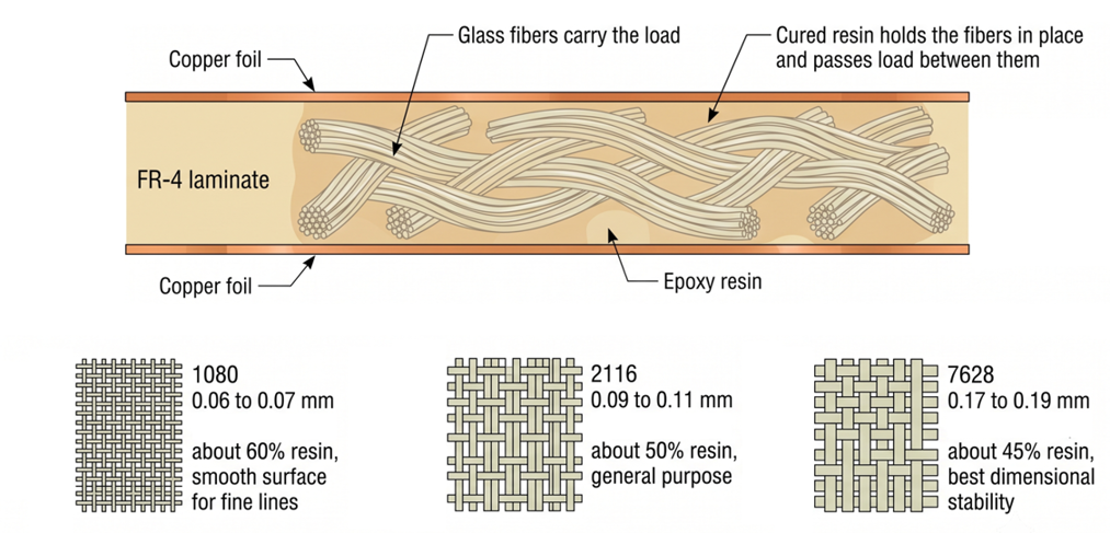
Those fibers come in standard weave styles defined by IPC-4412, and the style sets the thickness, surface smoothness, and how much a panel moves.
| Glass Style | Cured Thickness | Resin Content | Where It Gets Used |
|---|---|---|---|
| 1080 | 0.06 to 0.07 mm (2.4 to 2.8 mil) | Around 60% | Thin layers and fine-line outers, smooth surface |
| 2116 | 0.09 to 0.11 mm (3.5 to 4.3 mil) | Around 50% | General-purpose middle ground for multilayer builds |
| 7628 | 0.17 to 0.19 mm (6.7 to 7.5 mil) | Around 45% | Cores and thick boards, best dimensional stability |
Heavy glass cloth contains more glass and less resin, so it usually improves dimensional stability. Lighter cloth supports thinner dielectric layers and a smoother surface for fine-pitch traces. Fabricators combine cloth and prepreg styles to reach the finished thickness after pressing. Glass weave also gives the panel a direction: the board is stronger along the warp. That orientation can matter for a long, narrow PCB on the production panel. Thermal expansion also follows the material direction, and the next values show why board orientation matters in service:
In-plane expansion is controlled largely by the glass, typically around 14–17 ppm/°C, which is close to copper at about 17 ppm/°C. Through the thickness, however, the resin expands much more roughly 50–70 ppm/°C. That difference becomes important during reflow because it puts additional stress on the via barrels. The glass largely controls how the board behaves mechanically, while the resin has a much bigger influence on its thermal behavior.
Essential Features and Design Benefits of Rigid PCBs
Rigid PCB construction keeps a board flat through a 250 degree C oven and still flat after five years on a vibrating machine. Those are the features that matter in practice.
Key Rigid PCB Features That Ensure Structural Integrity
Three parts of the build carry the mechanical load:
- Cured core: A hardened sheet of glass and epoxy with copper on both faces, load-bearing the way a steel beam is in a building.
- Prepreg between layers: Glass cloth pre-loaded with partly cured resin, which, under heat and pressure, cures into one solid, so a ten-layer board behaves as a single piece.
- Plated through holes: Every barrel is a copper rivet tying the faces together, knitting the board in a way plain laminate is not.
Uneven copper distribution bends a panel as it cools after pressing because copper and resin shrink at different rates. A plane on one side and sparse routing on the other pull the board toward the copper-rich face. IPC-6012 allows 0.75% bow and twist on surface-mount boards. On a 200 mm (7.9 inch) board, that equals 1.5 mm (59 mil) of corner lift, enough to hold a fine-pitch package above its pads.
Case study: A batch of sensor boards came back with the 3.3 V rail pulled to 1.8 V. A 1206 ceramic capacitor sat 2 mm (79 mil) from a V-score line, one end cap in front of the other across the score. Snapping the panel by hand bent the board slightly and cracked the ceramic internally, where no camera could see it. Under biases that crack carbonized into a leakage path. To fix this: Pull ceramics 5 mm (197 mil) back from every break line, and turn them so both end caps sit along the score.
Electrical and Mechanical Benefits of Rigid PCB in Complex Assemblies
- The geometry remains constant in most electrical advantages of rigid construction, meaning that during service, the designed impedance, component alignment, and thermal paths remain constant as well.
- Controlled impedances: Trace width, copper thickness, and height above the reference plane determine the value of the trace impedance. Once laminated, that height remains the same – a 50-ohm line remains a 50-ohm line.
- Layer count without compromise: Builds run from 1 to 32 layers, so every high-speed signal can have a solid return plane beneath it.
- Density that suits modern packages: Trace and space down to 0.10 / 0.10 mm (4 / 4 mil) at 1 oz copper is what makes escape routing from a 0.5 mm pitch BGA possible.
- Heat spreading: FR-4 conducts heat poorly at about 0.3 W/mK, so copper does the work through solid planes and a via array under the hot part.
- Mechanical anchoring: TO-220 regulators, heatsinks, board-to-board connectors, shield cans, and tall electrolytics need a base that will not deflect.
- Repeatable assembly: The board rides a standard conveyor on its own edges, with no carrier and no special handling.
Rigid does not mean unbreakable. Because the substrate cannot stretch, excessive bending creates cracks instead. A 1.6 mm board bent 3 mm in a drop may crack a joint or via barrel and become intermittently faulty.
Architectural Comparison: Rigid vs Flexible PCBs
Flexible circuits replace the glass-reinforced epoxy panel with thin polyimide film, and every difference that follows starts there. Your decision turns on one question: must any part of the product bend, fold, or move repeatedly?
Mechanical Flexibility vs. Structural Stability and Load-Bearing Capacity
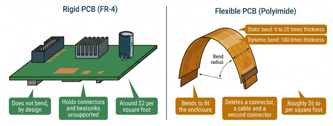
A rigid PCB holds its assigned shape. A flexible PCB follows the enclosure, which creates both its advantages and its limitations. Bend radius becomes the first constraint. IPC-2223 expresses that radius as a multiple of circuit thickness, with different factors for one-time and repeated bending during the product life.
- Static bending, folded at assembly and never moved again, allows 6 times the thickness for single-layer flex and 10 to 20 times for multilayer.
- Dynamic bending, flexing in service, demands 100 times the thickness for a single layer and 100 to 150 times for multilayer.
Example: A 0.2 mm (8 mil) double-sided flex folds to a 2 mm (79 mil) radius once at assembly. Flexing in service opens that radius to 20 mm (0.8 inch), which usually forces the mechanical design to change.
Electrodeposited foil is composed of columnar grains that crack when it is bent several times. The elongation of rolled-annealed foil is greater than that of the other, since the grains of the former foil are elongated, 15 to 40%, and the latter foil is only 5 to 15%. It lasts for more than one million flex cycles; electrodeposited foil fails at fewer than one thousand flex cycles.
| Attribute | Rigid PCB (FR-4) | Flexible PCB (Polyimide) | What It Means for Your Build |
|---|---|---|---|
| Bending | Does not bend, by design | 6 to 20 times thickness static, 100 times dynamic | Reserve enclosure space for the radius |
| Load bearing | Holds connectors and heatsinks unsupported | Needs a stiffener under every connector | Each adds material, a step, and cost |
| Copper foil | Electrodeposited, nothing moves | Rolled annealed for service flexing | Wrong foil looks fine, fails in months |
| Raw material | Around $2 per square foot | Roughly $6 to $60 per square foot | A 3x to 30x gap before processing |
| Field failure | Cracked joint or ceramic from the board flex | Copper fatigue at the bend, tear at the transition | The two fail for opposite reasons |
A desktop graphics card uses a rigid board to support a cooler weighing over one kilogram from its edge connector. A laptop hinge needs a flexible ribbon because no rigid board survives repeated motion reliably.
Cost Efficiency, Assembly Throughput, and Durability Trade-offs
Rigid PCBs usually cost less when compared square inch for square inch, but board price is not always the system price. A flexible PCB can recover its premium by removing connectors, cables, and separate assembly steps from the entire finished product and its enclosure.
Rigid boards are arranged on a rectangular production panel and separated using V-scoring or tab routing. You are therefore paying not just for the board itself, but also for the space it occupies on the panel and any unused material around it. A simple rectangle that nests tightly with other boards will usually use the panel much more efficiently than an L-shaped outline with the same finished area. A rigid board rides the rails of a standard pick-and-place line on its own edges, with no tooling. A flex circuit must be held flat on a machined aluminum carrier pallet and printed through a thinner stencil, around 0.1 mm (4 mil), against the 0.12 to 0.15 mm (5 to 6 mil) typical of rigid work, with squeegee pressure cut 15 to 25%.
- Choose rigid when the board sits still, carries connectors or heat, or ships in volume.
- Choose flex when the geometry genuinely requires bending.
Even experienced teams get the next part wrong:
Treating a one-time fold as dynamic bending wastes enclosure space. The 100 times thickness rule gets applied to a circuit folded once at assembly. Ask this practical question: Does the bend move after the case closes? If not, 6 to 20 times the thickness is correct and frees space.
Choosing flex only to save weight can make every connector support needlessly expensive. Each connector needs a stiffener bonded beneath it. Use this check: count the stiffeners, because three or more usually means rigid was cheaper.
Why JLCPCB is the Leading Global Choice for Precision Rigid PCB Fabrication
Selecting a rigid PCB fabricator comes down to two questions: can the supplier hold the tolerances your design assumes, and will board ten match board one?
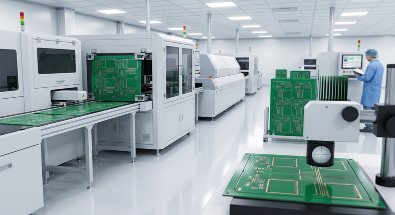
Fully Automated High-Speed Production Lines and Strict Tolerances
Automation improves consistency by reducing handling between process stations. Fewer manual transfers keep layer registration, hole position, and etch results inside a tighter window across successive panels and work shifts throughout routine production.
That consistency appears in the published tolerance list. Compare every listed limit with your design assumptions before uploading your manufacturing file package.
| Rigid PCB Parameter | JLCPCB Capability | What It Means for Your Design |
|---|---|---|
| Layer count | 1 to 32 layers | Room for dedicated planes on any design |
| Board thickness | 0.4 to 4.5 mm (16 to 177 mil) | 2.5 mm and above needs 12 or more layers |
| Thickness tolerance | Plus or minus 10% at 1.0 mm and above | A 1.6 mm order can arrive 1.44 to 1.76 mm |
| Trace and space | 0.10 / 0.10 mm (4 / 4 mil) at 1 oz, 0.16 mm at 2 oz | Heavy copper etches wider, needs wider gaps |
| Track width tolerance | Plus or minus 20% | Size the power traces in the low figure |
| Vias and holes | 0.15 mm hole, 0.25 mm via, 0.20 mm (8 mil) ring | Supports BGA escape routing and via-in-pad |
| Outline tolerance | Plus or minus 0.1 mm (4 mil) | Leave 0.2 mm of enclosure clearance |
One detail that can be a problem is the width of the trace. A 0.20 mm (8 mil) trace can end up being a 0.16 mm (6.3 mil) trace, which can result in a 20% decrease in copper area and a 20% increase in heating. If you are using the nominal width in your design, there is not much margin. Of course, FR-4 is not the only choice; rigid boards can be made with aluminum or copper cores; Rogers or PTFE is used with RF designs. Use a high Tg FR-4 or metal-core for higher temp. Popular finishes are HASL, ENIG, and OSP, depending upon board construction.
Industrial-Grade Quality Control: E-Test, AOI, and Reliable Global Shipping
The important thing is not how the machines work, but what it is that you get and what happens if a board fails inspection:
Rigid PCBs are electrically tested and inspected visually prior to shipment. This is particularly helpful with small orders, in which you could save a few dollars by not testing, but you may end up with larger issues down the road. When a board has an open or short against the netlist, it is scrapped and rebuilt instead of patched with a jumper. It's as easy as that; you get what you ordered, and it should be in working order.
Packaging is another important factor: boards are vacuum sealed and contain desiccant to prevent the surface finish from being affected by humidity. Especially for OSP or immersion finishes, which can become solderless if exposed to moisture. Express shipping is more expensive but faster, and economy is slower. There are extra time buffers in case of customs, as they may require additional time depending on the destination.
FAQ about Rigid PCB
Q: What is a rigid PCB?
A rigid PCB is a circuit board built on a hard substrate, almost always woven glass cloth in epoxy resin known as FR-4, designed never to bend. It holds every trace, pad, and component in a fixed position.
Q:Why is 1.6 mm the standard rigid PCB thickness?
It is a convention that predates most modern electronics, and it balances well. At 1.6 mm (63 mil), a board resists sag, fits standard card slots, and stays economical to build.
Q: What is the real difference between rigid and flexible PCBs?
Rigid boards use a glass-reinforced epoxy panel and carry mechanical load, while flexible boards use thin polyimide film and bend to fit a shape. Flex costs several times more per unit area and needs stiffeners under connectors.
Q: Does JLCPCB offer rigid polyimide boards?
No. Rigid builds run on FR-4, single-layer aluminum core, single-layer copper core, or Rogers and PTFE for RF. For high temperature work, high Tg FR-4 or a metal core is the practical route.
Conclusion
A rigid PCB is a rigid PCB because it doesn't move. Glass woven in flexes FR-4 to about 20 to 24 GPa and thickness cubes that to an impedance, footprints, and heat paths that remain where you calculated them, and a platform emerges. That's also the forthright end of the flex comparison. A flexible circuit is not a better board; it is a different structural option that requires the use of multiple times the material cost and gives up load-bearing capability for shape.
So specify it deliberately. Pick thickness for the mechanical job, design to the worst end of every tolerance, and keep ceramics away from break lines. When the design is settled, upload your Gerbers for an instant quote and see what those choices cost.

Popular Articles
• Understanding the Basics of Electronic Devices and Circuits
• Understanding Digital Circuit Timing: Setup Time, Hold Time, Contamination Delay & Clock Skew
• PCBs Explained: A Simple Guide to Printed Circuit Boards
• Guide to the Top 10 Commonly Used Electronic Components
• Digital 101: Fundamental Building Blocks of Digital Logic Design
Keep Learning
Polyimide Flex PCB: A Complete Guide for Engineers
A polyimide flex PCB can be folded about 285,000 times when the base film is 25 µm (1 mil) thick. Make that film 75 µm (3 mil), and the same MIT fold test gives up near 6,000 cycles. Bending is a strain problem, not a material problem. Copper sits above the center of the stack, so a bend forces it to stretch around the longer outer path. Figure 1: A polyimide flex circuit folded tight, with a stiffener holding the connector A thicker stack places the copper farther out, resulting in more stretch at th......
Flex PCB Bend Radius: Calculation, Minimum Radius & Design Guidelines
Flex PCB bend radius is the one dimension on an FPC that no design rule check will catch. Bend the circuit tighter than its material allows; the outer copper stretches from its elongation limit, and then it cracks. Figure 1: A flex circuit formed around a mandrel, with bend radius and stack thickness A flex circuit bends around a neutral axis near the middle of its stack. Copper below that line is squeezed, and copper above it is pulled. So the further a layer sits from the line, the harder it is to w......
Flexible Circuit Connector: Types, Features & Selection Guide
A flexible circuit connector clamps onto the bare copper at the end of a flex circuit, so nothing is soldered at that joint. The tail slides into the housing, and an actuator presses a row of spring contacts onto the pads. Every connector is built around one tail thickness. TE's 0.5 mm pitch 2328702 family expects 0.30 mm (12 mil) of flex, because the contact beams are deflected by exactly that dimension. Figure 1: Cross-section of a 0.5 mm pitch FPC connector with the tail inserted Feed it a bare sin......
FPC vs FFC: Understanding the Key Differences Between Flexible Circuit Technologies
The FPC vs FFC decision is really a question about how the copper was made. An FFC consists of flat copper strips laminated between two PET films. Every conductor runs straight from end to end at one fixed pitch, because nothing in that process can make a trace turn or branch. An FPC starts as copper-clad polyimide and is etched exactly like a rigid board. Traces can turn, taper, split onto a second layer, and land under a soldered component. The finished circuit can be as thin as 0.1 mm (4 mil). Figu......
A Comprehensive Guide to Capacitor ESR: What It Is, Good Values, and How to Measure It
Key Takeaways Definition: Capacitor ESR (equivalent series resistance) is the single resistance that represents the losses inside a real capacitor, from its electrodes, terminations, electrolyte, and dielectric. Why It Matters: Ripple current flowing through the ESR produces a ripple-voltage step on the supply rail and I²R heating in the capacitor, which limits the capacitor's ripple-current rating and service life. Conditions Matter: ESR varies with frequency, temperature, capacitance, case size, and......
Understanding IPC-6012 Standards for High-Reliability Rigid PCB Fabrication
Key Takeaways IPC-6012 vs. IPC-A-600: IPC-6012 is the binding specification, while IPC-A-600 is only for visual reference. Class 2 vs. Class 3: Class 3 requires thicker copper (25μm vs. 20μm) and zero plating voids. Coupon Verification: Quality is tested by microsectioning panel coupons after thermal stress. Upfront Callout: Specify the class on drawings upfront; boards cannot be upgraded later. IPC-6012 is the line on your fabrication drawing that decides what your supplier is allowed to ship. Most d......