Understanding Industrial PCB Production:Materials, Manufacturing Processes, and JLCPCB Capabilities
14 min
- What is Industrial PCB Production?
- Importance of Industrial PCB Production
- Key Substrates and Materials in Industrial PCB Manufacturing
- Types of PCBs in Industrial Production
- Step-by-Step Industrial PCB Manufacturing and Assembly Workflow
- Solder Mask and Silkscreen Application
- Key Challenges in Industrial PCB Fabrication and JLCPCB Solutions
- Primary Industrial Applications of PCBs
- Future Trends in Industrial PCB Production
- Internet of Things (IoT) and Smart Manufacturing:
- FAQ about Industrial PCB Production
- Conclusion
Key Takeaways
- Layer Capabilities: Supports up to 32-layer Rigid and 28-layer HDI PCBs (Rigid-Flex unsupported).
- Industrial Materials: High-Tg FR-4 (Tg 170°C), Aluminum cores, and Rogers RF laminates.
- Free POFV Technology: Free resin-filled via-in-pad provided for 6–32 layer designs.
- Turnkey Assembly: Integrated online DFM checks and automated SMT assembly.
Nearly all electronic devices rely on Printed Circuit Boards (PCBs) as their foundational backbone, supporting and interconnecting active and passive components. As industrial sectors rapidly evolve, the demand for high-reliability, high-density, and cost-effective mass-produced PCBs has grown exponentially. Industrial PCB production encompasses large-scale fabrication for demanding applications including automotive systems, aerospace, industrial automation, medical devices, and telecommunications. This comprehensive guide explores key materials, step-by-step manufacturing workflows, design best practices, and how JLCPCB's advanced fabrication capabilities empower modern industrial hardware design.
What is Industrial PCB Production?
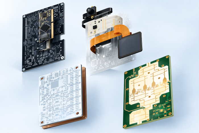
Industrial PCB production refers to the precision mass fabrication of printed circuit boards engineered to meet strict operational requirements across diverse industrial sectors. Unlike standard consumer-grade PCBs, industrial-grade boards must guarantee continuous performance under elevated thermal, mechanical, and environmental stress. Consequently, they are manufactured in accordance with strict international IPC standards (such as IPC Class 2 and IPC Class 3). The industrial production lifecycle spans schematic logic verification, DFM (Design for Manufacturability) analysis, high-precision layering, automated fabrication, and rigorous quality inspection.
Importance of Industrial PCB Production
The fabrication of premium PCBs is crucial for ensuring the uptime, safety, and efficiency of mission-critical industrial electronics. Key factors driving industrial PCB manufacture include:
1. Ensuring Extreme Reliability and Durability
Industrial PCBs operate in harsh environments subject to thermal cycling (-40°C to +125°C), high vibrations, electrostatic discharge, and humidity. Utilizing High-Tg FR-4 substrates (e.g., Tg 170°C) and heavy copper layers (up to 2 oz) ensures structural stability and prevents thermal delamination or via plating cracks during prolonged operations.
2. Enabling High-Density Interconnects (HDI) and Miniaturization
As industrial automation controllers and smart sensors become more compact, high-density packaging is essential. Industrial PCB fabrication leverages High-Density Interconnect (HDI) technology—utilizing laser-drilled microvias down to 0.15 mm and fine trace/space capabilities down to 3.5 mil (0.09 mm)—to pack maximum logic into minimal board real estate without thermal or signal degradation.
3. Supporting Complex Multilayer Signal Routing
Modern industrial systems involve high-speed data acquisition and multi-axis control requiring complex multilayer stackups (4 to 20 layers). Advanced multi-layer techniques ensure signal integrity, minimize electromagnetic interference (EMI), and maintain controlled impedance matching for high-speed industrial protocols.
Key Substrates and Materials in Industrial PCB Manufacturing
The thermal, electrical, and mechanical performance of an industrial PCB depends fundamentally on its substrate materials and metallic layers:
Conductive Layers (Copper Foil): High-purity electrodeposited copper foil forms traces and planes. Standard copper weights range from 0.5 oz (17.5 µm) for fine signal routing to 1 oz and 2 oz (70 µm) for high-current power distribution.
Standard & High-Tg Substrates (FR-4): Glass-reinforced epoxy laminates. While standard FR-4 (Tg 130–140°C) suits general electronics, industrial environments require High-Tg FR-4 (Tg 170°C) to withstand lead-free reflow temperatures (peak ~260°C) and elevated continuous operating temperatures.
Thermal Metal Cores (Aluminum PCBs): Metal core PCBs (MCPCBs) featuring 1.0mm–1.6mm aluminum substrates provide superior heat dissipation for high-power industrial LED lighting, power conversion, and motor drives.
High-Frequency Laminates (Rogers & PTFE): Hydrocarbon/ceramic laminates used for RF, microwave, and high-speed industrial radar applications requiring low dielectric loss and stable dielectric constant.
Flexible Laminates (Polyimide): Used in flexible and rigid-flex PCBs where dynamic bending or extreme spatial constraints are present.
Solder Mask & Silkscreen: High-durability liquid photoimageable (LPI) solder masks protect underlying copper from oxidation and solder bridging during assembly (available in Green, Red, Blue, Black, White, Yellow, Purple). High-precision silkscreen (line width down to 0.10 mm) applies component reference marks.
Table 1: JLCPCB Industrial PCB Material Specifications & Capabilities
| Material Type | Tg / Thermal Conductivity | Standard Thickness Options | Copper Weight Range | Primary Industrial Applications |
|---|---|---|---|---|
| Standard FR-4 | Tg 130 – 140°C | 0.4 mm – 4.5 mm | 0.5 oz, 1 oz, 2 oz | General industrial control, IoT gateways |
| High-Tg FR-4 | Tg 170°C | 0.8 mm – 4.5 mm | 1 oz, 2 oz | High-temperature controllers, Automotive ECUs |
| Aluminum Core | 1.0 – 2.0 W/m·K | 0.8 mm, 1.0 mm, 1.2 mm, 1.6 mm | 1 oz | High-power LED lighting, Motor drives, Inverters |
| Rogers (RF) | RO4350B / RO4003C (Dk 3.38–3.48) | 0.254 mm – 1.524 mm (FR-4 Hybrid supported) | 0.5 oz, 1 oz | 5G telecom, Industrial radar, RF sensors |
| Flexible (FPC) | High Thermal Stability (PI) | 0.07 mm – 0.45 mm (1–4 Layers) | 1/3 oz, 0.5 oz, 1 oz | Medical devices, Robotic joints, Compact sensors |
Types of PCBs in Industrial Production
Industrial electronics incorporate various PCB structural configurations optimized for mechanical, thermal, and spatial demands:
Single-Sided and Double-Sided PCBs: Entry-level boards with conductive copper on one or both sides, ideal for power supplies and baseline sensor modules.
Standard Rigid Multilayer PCBs (1 to 32 Layers): Multilayer boards bonded with prepreg insulation. Standard rigid PCBs support complex power distribution and impedance-controlled signal routing. JLCPCB supports up to 32 layers with free resin-filled via-in-pad (POFV) technology for 6 to 32-layer designs.
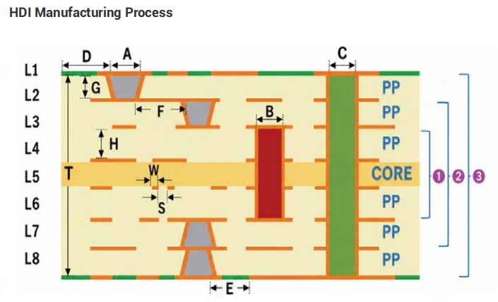
High-Density Interconnect (HDI) PCBs (4 to 28 Layers): Designed for dense BGA components and high-speed processors, HDI PCBs utilize microvias (0.15 mm laser drill), blind/buried vias, and advanced stackups. JLCPCB manufactures advanced HDI boards up to 28 layers.
Flexible PCBs (FPC, 1 to 2 Layers): Built on flexible polyimide (PI) substrates for dynamic bending and space-constrained applications (e.g., wearable medical sensors, robotic joints). Note: While industry applications sometimes utilize Rigid-Flex hybrids, JLCPCB currently focuses on ultra-reliable standalone Rigid (up to 32L) and Flex (up to 2L) manufacturing.
Table 2: Calibrated JLCPCB Manufacturing Capabilities by PCB Type
| PCB Type | Max Layer Count | Min Trace / Space | Min Drill Diameter | Surface Finish Options | Special Features / JLCPCB Capabilities |
|---|---|---|---|---|---|
| Standard Rigid PCB | 1 - 32 Layers | 3.0 mil / 3.0 mil | 0.15 mm (Mechanical) | HASL, Lead-free HASL, ENIG, OSP | Free resin-filled via (POFV) for 6–32 layers, Castellated holes, Edge plating |
| HDI PCB | 4 - 28 Layers | 3.0 mil / 3.0 mil | 0.15 mm (Laser Microvia) | ENIG | 1–3 Order & Any-layer HDI, Blind & Buried Vias, Via-in-Pad (POFV) |
| Flex PCB | 1 - 2 Layers | 3.5 mil / 3.5 mil | 0.20 mm | ENIG | Polyimide / FR4 stiffener, 3D dynamic bending, ultra-thin profile |
| Aluminum PCB | 1 Layer | 5.0 mil / 5.0 mil | 0.65 mm | HASL, Lead-free HASL | Direct thermal dissipation metal core (1.0–2.0 W/m·K) |
Step-by-Step Industrial PCB Manufacturing and Assembly Workflow
Industrial PCB production demands high automation and strict quality oversight across every manufacturing stage:
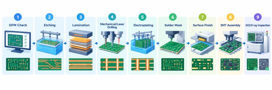
1.DFM Analysis & CAD Processing: Engineering tools perform automated Design for Manufacturability (DFM) checks to verify clearance, minimum trace widths, drill dimensions, and stackup feasibility.
2.Inner Layer Patterning & Etching: For multilayer boards, core copper laminates are photo-imaged and chemically etched to create internal conductive traces.
3.Lamination & Bonding: Inner layers are interleaved with insulating prepreg sheets and bonded under heat and pressure into a solid multilayer board.
4.Precision Drilling (Mechanical & Laser): High-speed CNC machines drill through-holes (down to 0.20 mm), while UV/CO2 laser systems drill microvias (0.15 mm) for HDI stackups.
5.Copper Plating (Barrel Metallization): Chemical copper deposition and electroplating coat the hole walls with 20–25 µm of copper, establishing reliable inter-layer electrical connectivity.
6.Solder Mask Coating & Curing: Liquid Photoimageable (LPI) solder mask is applied over outer copper layers and UV-cured to protect traces from ambient oxidation and prevent solder bridging during reflow.
7.Silkscreen Printing: High-precision silkscreen ink is printed over the cured solder mask layer to display component designators, polarities, and logos.
8.Surface Finishing: Exposed pads receive protective finishes—such as ENIG (Electroless Nickel Immersion Gold) for ultra-flat BGA pads or Lead-Free HASL—to preserve solderability.
9.SMT Component Assembly & Inspection: Automated SMT pick-and-place machines mount components (down to 0201/0402 packages and fine-pitch BGAs). Assemblies undergo Automated Optical Inspection (AOI), 3D X-ray inspection for hidden BGA solder joints, and electrical flying probe testing.
Solder Mask and Silkscreen Application
Following a silkscreen for labels and designators, a solder mask is placed to guard the copper traces.
Component Assembly:
Automated machinery solder Surface Mount Devices (SMD) and other components onto the board. Reliable connections and minimizing mistakes depend on this stage being important.
Testing and Quality Control:
The last stage is thorough testing to guarantee that the PCB satisfies industry requirements and operates as expected using Automated Optical Inspection (AOI), X-ray inspection, and electrical testing.
Key Challenges in Industrial PCB Fabrication and JLCPCB Solutions
Manufacturing industrial-grade boards presents distinct engineering hurdles:
Miniaturization & High Density: Modern ICs require tighter tolerances. Solution: JLCPCB utilizes HDI laser microvias (0.15 mm) and via-in-pad (POFV) technology to route complex BGA signals cleanly within compact board footprints.
Thermal Management: Inadequate thermal dissipation degrades components. Solution: Designers leverage JLCPCB’s Aluminum core substrates (1.0-2.0 W/m·K) and 2 oz heavy copper layers combined with thermal via arrays to transfer heat away from power transistors.
High-Speed Signal Integrity: Signal degradation, crosstalk, and EMI can corrupt data. Solution: JLCPCB provides controlled impedance calculations (Microstrip 20–90Ω, Differential 50–150Ω) and supports Rogers high-frequency laminates.
Cost Efficiency vs. Quality: Balancing budget constraints with industrial longevity is challenging. Solution: JLCPCB offers transparent pricing, free ENIG/Via-in-pad promotions on 6-layer boards, and automated online DFM checks to lower manufacturing risks and total system costs.
Primary Industrial Applications of PCBs
Industrial PCBs serve as the indispensable infrastructure driving mission-critical hardware across diverse high-reliability sectors. Unlike commercial PCBs, industrial-grade boards are custom-engineered to maintain uninterrupted operation under extreme vibration, chemical exposure, and intense thermal fluctuations:
Automotive Systems & Electric Vehicles (EV):
Modern automotive architectures rely heavily on industrial PCBs for Engine Control Units (ECUs), Advanced Driver Assistance Systems (ADAS) radar modules, and battery management systems (BMS) in electric vehicles. These applications demand High-Tg FR-4 substrates, heavy copper layers for high power distribution, and ENIG surface finishes to resist moisture, vibration, and elevated under-hood temperatures.
Industrial Automation, Power Electronics & Robotics:
Industrial automation is the largest single sector for heavy-duty PCBs. From Programmable Logic Controllers (PLCs) and motor drives to industrial robotic joint actuators and smart IIoT gateways, PCBs must handle high currents and multi-axis real-time signal processing. JLCPCB’s 1–32 layer rigid PCBs with thick copper (up to 2 oz) and free via-in-pad (POFV) technology ensure compact and durable power electronics layout.
Aerospace, Avionics & Defense:
Aerospace systems—such as flight control computers, satellite communications, and military radar equipment—demand zero-defect reliability. PCBs in this sector must satisfy strict IPC Class 3 quality guidelines, featuring High-Tg materials and controlled impedance stackups capable of enduring extreme thermal shock and atmospheric radiation.
Telecommunications & 5G Infrastructure:
Industrial telecom equipment including 5G base stations, optical transceivers, and network switches requires high-speed data transfer with low latency. These designs frequently utilize Rogers high-frequency laminates ($D_k$ 3.38–3.48) and multi-layer HDI stackups (up to 28 layers) to minimize signal loss (Df) and crosstalk at gigahertz frequencies.
Medical Devices & Advanced Diagnostics:
Medical diagnostic machines, surgical robotics, and MRI scanners require ultra-precise signal integrity and high-density packaging. Flexible PCBs (FPC) and high-layer HDI rigid boards enable lightweight, highly integrated hardware for life-critical medical devices.
Future Trends in Industrial PCB Production
The industrial PCB sector is being shaped by cutting-edge innovations:
Advanced HDI & Ultra-Fine Lines: Increased density driven by 5G and AI requires sub-3 mil trace resolution, multi-layer microvias, and up to 28-layer HDI capabilities.
Smart Automation & AI Quality Control: Factories are integrating AI-powered optical inspection (AOI) and 3D X-ray systems to automatically detect manufacturing defects at micro scales.
Sustainable Eco-Friendly Manufacturing: Transitioning to lead-free soldering, eco-friendly chemical recycling, and RoHS-compliant materials reduces carbon footprints.
Internet of Things (IoT) and Smart Manufacturing:
Demand for smart PCBs able to handle communication and data processing in connected devices is being prompted by the expansion of the Internet of Things (IoT). Furthermore, applied are smart manufacturing methods to improve supply chain management, track inventory in real-time, and raise production efficiency.
Enhanced Testing and Quality Assurance:
Enhanced testing and quality assurance techniques are being developed as PCBs grow more complicated. Using advanced inspection technologies including 3D X-ray imaging and machine learning algorithms, flaws are found and highest quality requirements are guaranteed to be fulfilled.
FAQ about Industrial PCB Production
Q: What is a blind via in a PCB, and how does it differ from a buried via?
A blind via connects an outer layer to one or more inner layers without passing through the entire board, so it is visible only on one side. In contrast, a buried via connects internal copper layers only and does not extend to either outer surface. Both are used together in HDI PCBs to save routing space.
Q: How do blind vias improve high-speed signal integrity?
Because blind vias only penetrate part of the stackup rather than passing all the way through, they significantly shorten or eliminate the unused via stub. Shorter stubs decrease impedance discontinuities and resonances, which is essential for preserving signal quality in multi-gigabit interfaces like DDR and PCIe.
Q: What is the recommended aspect ratio for blind microvias?
For laser-drilled blind microvias, you should aim for a depth-to-diameter aspect ratio of around 0.75:1, with 1:1 treated as the maximum limit. Keeping within this ratio ensures that plating chemistry reaches the bottom of the hole for a uniform, void-free copper fill.
Q: Can blind vias be placed directly inside component pads (via-in-pad)?
Yes. When blind microvias are filled with copper and capped, they can be integrated directly into SMT pads (via-in-pad). This design choice saves board space, improves heat dissipation, shortens current pathways, and prevents solder leakage during assembly.
Q: Are blind vias always drilled using lasers?
Most blind vias in modern HDI designs are microvias created using UV or CO2 lasers because laser drilling offers the high precision and depth control required for small hole diameters. While larger blind vias can technically be formed with controlled-depth mechanical drilling, laser drilling is the dominant method for fine-pitch BGA routing.
Conclusion
Industrial PCB production is the foundational pillar supporting modern technology across automotive, aerospace, industrial automation, and telecommunications. By selecting the optimal substrates, adhering to DFM standards, and leveraging state-of-the-art manufacturing techniques, engineers can build resilient, high-performance hardware.
As a global leader in PCB fabrication and assembly, JLCPCB simplifies industrial hardware development. Offering 1 to 32-layer Rigid boards, up to 28-layer HDI technology, High-Tg laminates, surface finishes like ENIG, and fully automated SMT assembly, JLCPCB delivers industrial-grade reliability with fast turnaround times and competitive pricing.
Ready to bring your industrial design to life? Upload your Gerber files to JLCPCB today for an instant online quote!
Popular Articles
• Understanding the Basics of Electronic Devices and Circuits
• Understanding Digital Circuit Timing: Setup Time, Hold Time, Contamination Delay & Clock Skew
• PCBs Explained: A Simple Guide to Printed Circuit Boards
• Guide to the Top 10 Commonly Used Electronic Components
• Digital 101: Fundamental Building Blocks of Digital Logic Design
Keep Learning
Polyimide Flex PCB: A Complete Guide for Engineers
A polyimide flex PCB can be folded about 285,000 times when the base film is 25 µm (1 mil) thick. Make that film 75 µm (3 mil), and the same MIT fold test gives up near 6,000 cycles. Bending is a strain problem, not a material problem. Copper sits above the center of the stack, so a bend forces it to stretch around the longer outer path. Figure 1: A polyimide flex circuit folded tight, with a stiffener holding the connector A thicker stack places the copper farther out, resulting in more stretch at th......
Flex PCB Bend Radius: Calculation, Minimum Radius & Design Guidelines
Flex PCB bend radius is the one dimension on an FPC that no design rule check will catch. Bend the circuit tighter than its material allows; the outer copper stretches from its elongation limit, and then it cracks. Figure 1: A flex circuit formed around a mandrel, with bend radius and stack thickness A flex circuit bends around a neutral axis near the middle of its stack. Copper below that line is squeezed, and copper above it is pulled. So the further a layer sits from the line, the harder it is to w......
Flexible Circuit Connector: Types, Features & Selection Guide
A flexible circuit connector clamps onto the bare copper at the end of a flex circuit, so nothing is soldered at that joint. The tail slides into the housing, and an actuator presses a row of spring contacts onto the pads. Every connector is built around one tail thickness. TE's 0.5 mm pitch 2328702 family expects 0.30 mm (12 mil) of flex, because the contact beams are deflected by exactly that dimension. Figure 1: Cross-section of a 0.5 mm pitch FPC connector with the tail inserted Feed it a bare sin......
FPC vs FFC: Understanding the Key Differences Between Flexible Circuit Technologies
The FPC vs FFC decision is really a question about how the copper was made. An FFC consists of flat copper strips laminated between two PET films. Every conductor runs straight from end to end at one fixed pitch, because nothing in that process can make a trace turn or branch. An FPC starts as copper-clad polyimide and is etched exactly like a rigid board. Traces can turn, taper, split onto a second layer, and land under a soldered component. The finished circuit can be as thin as 0.1 mm (4 mil). Figu......
A Comprehensive Guide to Capacitor ESR: What It Is, Good Values, and How to Measure It
Key Takeaways Definition: Capacitor ESR (equivalent series resistance) is the single resistance that represents the losses inside a real capacitor, from its electrodes, terminations, electrolyte, and dielectric. Why It Matters: Ripple current flowing through the ESR produces a ripple-voltage step on the supply rail and I²R heating in the capacitor, which limits the capacitor's ripple-current rating and service life. Conditions Matter: ESR varies with frequency, temperature, capacitance, case size, and......
Understanding IPC-6012 Standards for High-Reliability Rigid PCB Fabrication
Key Takeaways IPC-6012 vs. IPC-A-600: IPC-6012 is the binding specification, while IPC-A-600 is only for visual reference. Class 2 vs. Class 3: Class 3 requires thicker copper (25μm vs. 20μm) and zero plating voids. Coupon Verification: Quality is tested by microsectioning panel coupons after thermal stress. Upfront Callout: Specify the class on drawings upfront; boards cannot be upgraded later. IPC-6012 is the line on your fabrication drawing that decides what your supplier is allowed to ship. Most d......