The Hardware Development Process: From Concept to a Finished Electronic Product
14 min
- Hardware Requirements and System Analysis
- Component Selection for hardware development
- Hardware Schematic Design and Verification
- PCB Design and Layout for Hardware Development
- PCB Fabrication and Assembly in Hardware Development Process
- Flashing the Software System
- Hardware Testing and Validation
- FAQs about Hardware Development Process
- Conclusion
Key Takeaways
- A structured hardware development process turns concepts into functional products through key development stages.
- Proper PCB design balances performance, manufacturability, and reliability.
- Early manufacturing considerations help reduce risks and improve prototype success.
- A reliable PCB partner enables smoother transitions from design to production.
Every electronic device you have ever used began as a single idea. A desk lamp that brightens with a tap, a wireless earbud, a controller inside a supercomputer — each one traveled the same road from a blank page to a working, manufacturable product.That road is the hardware development process, and its quality determines whether a product meets its performance, cost, and reliability targets. Understanding each stage—from system analysis and component selection to PCB manufacturing and final validation—helps teams identify risks early and move from concept to a manufacturable product.
Hardware Requirements and System Analysis
Define Requirements and Functional Blocks
The design begins not as a schematic but as a question: what must this product do, for whom, under what conditions, and within what constraints? System-level analysis answers that question by decomposing the product into functional blocks — power, computation, sensing, human interface, communication, and actuation — and defining how those blocks exchange data and energy. Each block gets a clear responsibility and a defined interface. Every requirement that enters the design is written down and traceable, whether its source is a customer brief, a regulatory rule, or an internal standard, so that a late decision never silently touches ten other blocks at once.
Establish Power, Thermal, and Cost Budgets
Two numbers govern almost every downstream choice. The power budget totals the current each block draws, sizes the battery or supply rail, and sets the efficiency each converter must reach. The thermal budget follows from it: every dissipated watt must be moved, through air, copper, and enclosure, without pushing any component past its limit. The cost budget converts those choices into a per-unit price target. A design that closes its nominal power budget but ignores peak load, or that fits the electronics but not the heat it generates, fails here rather than in the schematic.
Verify Feasibility and Lock the Architecture
With the blocks defined and the budgets closed, the team confirms the project is buildable. Manufacturing tolerances, tooling, certification timelines, and per-unit cost are estimated against the target, and the architecture is frozen so later stages proceed from a stable baseline. This is the earliest point at which an honestly unbuildable concept is allowed to stop — far cheaper to terminate a feasibility study than to cancel a hardware program after tooling is paid for.
Component Selection for hardware development
Choose the Functional IC
The heart of the design is the functional IC: the microcontroller or SoC that coordinates everything, the power-management device, the wireless transceiver, or the motor driver. Datasheet headline numbers matter, but so do real-world behavior and headroom. A processor that hits its clock target on paper may need margin for temperature and voltage droop; a regulator with a tight efficiency spec may be fragile under a transient load. Engineers evaluate the part against the actual operating envelope of the product, not against the marketing page.
Match Supporting Components to Engineering Budgets
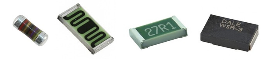
Less glamorous but equally decisive are the supporting components — resistors, capacitors, inductors, connectors, and protection devices — and each is chosen against the budgets set in the previous stage. Tolerances, temperature coefficients, and rated lifetimes must live inside the thermal budget and deliver the expected behavior; cost-wise, these parts dominate the bill-of-materials by count, so their total must fit the cost budget even though each one is cheap. A decoupling capacitor with poor ESR performance or an input fuse undersized for inrush can silently degrade a design that looked correct in simulation. Component selection is therefore a systems activity, not a one-part decision.
Mitigate Cost and Supply-Chain Risk
A superb component is only as good as its availability. Lead times, minimum order quantities, end-of-life announcements, and single-source exposure are part of the evaluation. Engineers prefer parts with second sources or documented lifecycles, and they review the bill of materials for parts that could become unobtainable mid-program. Value engineering balances a premium part against a cheaper one that meets the requirement with less margin, and early purchasing with a forecast converts a cost estimate into an actual price. Hardware cannot be patched over the air the way software can, so supply-chain diligence is a core part of component selection rather than an afterthought.
Hardware Schematic Design and Verification
Design the Power Architecture and On-Sequence
Power lands first because every other block depends on it. The team defines the input source and voltage range, maps the derived rails, chooses converter topologies, and lays out the power-on sequencing — which rail must come up before which. Protections, reverse-polarity guards, and decoupling are specified here. Power errors are the most expensive to find later, so this stage gets disproportionate scrutiny.
Compute Values and Define Signal Interfaces
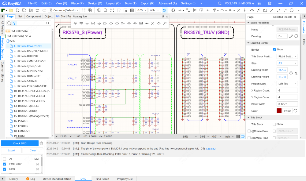
Each component value is derived from an explicit calculation or a datasheet recommendation, and every signal that crosses the sheet boundaries needs well-defined electrical characteristics: levels, impedance, filtering, pull states, and protection. A bias resistor, a feedback network, an RC filter's cutoff, a crystal's load capacitance, pull-up values, and digital termination are each computed and documented so that a reviewer can re-derive them. The interface contract defined here is what keeps the blocks that meet on the board from misbehaving.
Verify With Simulation and Design Review
Before the netlist leaves the screen, the design is exercised. Power stages and analog paths run through simulation to expose oscillation, under-rated parts, and marginal stability, while an electrical rules check (ERC) sweeps for floating pins, shorted nets, and disconnected symbols. A structured design review, ideally by an engineer not on the authorship team, then closes the stage: the reviewer re-derives critical values, checks the power budget against what the schematic actually draws, and looks for the load that was assumed away. Review findings are the cheapest corrections the product will ever receive.
PCB Design and Layout for Hardware Development
Plan the Layer Stackup and Component Placement
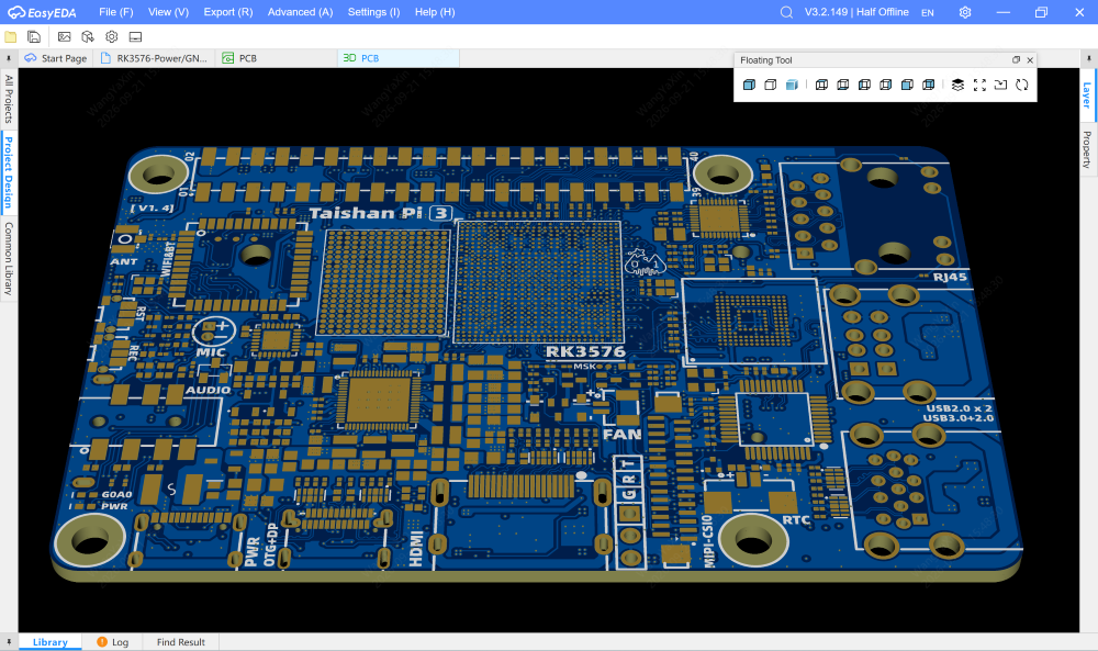
The stackup is the bridge between the schematic and the physical board. Designers choose the number of layers, the copper weights, and the placement of power and ground planes — decisions that shape signal return paths, thermal spreading, and impedance control. Placement then turns electrical and thermal intent into physical reality: high-speed logic is kept near its loads and decoupling, switching regulators are separated from sensitive analog or RF circuitry, and heat-generating parts are spread and given copper or airflow to sink their dissipation. Placement also respects manufacturing, aligning components to assembly directions and clearances that allow soldering.
Route Traces for Current, Impedance, and Reliability
Routing translates the schematic into copper while honoring three masters. Trace width is sized to the current it carries and the temperature rise it may tolerate. Impedance-sensitive connections — differential pairs, clocks, high-speed buses — are width-controlled, length-matched, and kept close to their reference plane so that a high-speed transition still arrives clean (signal integrity) and every rail stays within tolerance when loads change abruptly (power integrity). And the routing respects the mechanics of manufacturing: clearances, minimum widths, and drilling limits that let the board actually be made. On top of that, the layout should be legible to a human and managed as a potential radiator — controlling loop areas, return paths, and filtering at I/O boundaries so the board stays electromagnetically clean — so that it can be certified and serviced years later.
Validate Against Design Rules and Manufacture (DFM/DRC)
Before release, the design is checked against the fabricator's rules: minimum trace, pad, and drill sizes; annular rings; solder-mask and silkscreen clearances. Design-for-manufacture (DFM) reviews add panelization, fiducials, and component orientation that let a board be built reliably in volume. Any gap between the design and the shop's capability will otherwise surface as failures that push cost onto quality and after-sales support.
PCB Fabrication and Assembly in Hardware Development Process
Select a Capable Fabricator
Fabrication turns the design files into physical copper, and the fabricator's quality is now part of the design. The team confirms the shop can hold the required tolerances, layer count, and impedance control, and evaluates its track record for on-time delivery and quality. A fabricator that returns boards which look right but fail impedance or reflow tests quietly undermines the entire verification program downstream.
For projects that require a reliable PCB manufacturing partner, JLCPCB provides PCB fabrication and assembly services for different design and production requirements. You can review the available manufacturing capabilities and submit your design for a quote through JLCPCB.
Assemble and Bring Up the First Prototype
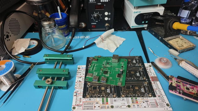
The first boards back from the fab are bare; the team assembles them, often by hand at prototype volume. Full reflow and machine placement may appear only at the next quantity step. Hand-soldering is fast and flexible but introduces its own failures — solder bridges, cold joints, tombstoned components — that no electrical design can prevent, so the assembly step carries its own verification beyond the schematic's. Panelization and stencil alignment, decided during the layout stage, matter here to keep prototypes representative of production. Work then progresses from the power rails outward — clocks, reset, core, peripherals — so each block that comes up correctly is verified before the next is enabled.
Run Power-On and Continuity Checks
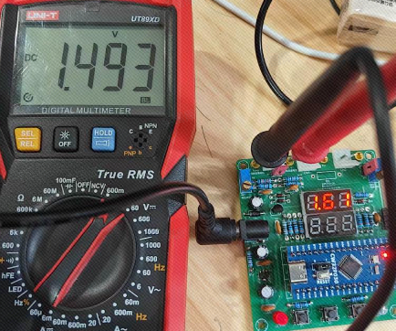
The first electrical contact is deliberately cautious. Engineers verify the board is not shorted rail-to-ground, confirm key signals show no unintended opens, and then bring up power in a documented sequence while monitoring current. Every measurement is compared against the schematic's expectation. Assembly defects are separated from design defects here, at the earliest moment, before any firmware exists to confuse the picture, turning the populated board from a gamble into a known-good assembly the software team can trust.
Flashing the Software System
Flash and Debug the Firmware
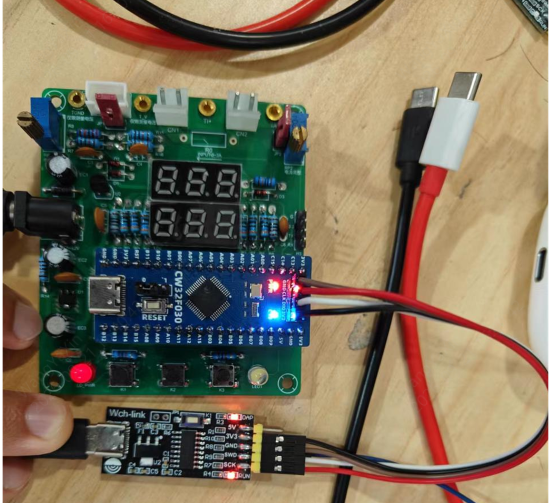
A board without code is inert silicon. The earliest software is bring-up code, partitioned into layers — a bootloader, low-level drivers, a hardware-abstraction layer, and the application itself — that exercise each peripheral one at a time, check the silicon against the datasheet, and verify clock trees and power states. This is delivered through a debugger attached via JTAG or a serial-wire debug port, which allows single-stepping and register inspection. The product path differs: final units load firmware through a bootloader over UART, USB, or SPI, or update it over the air in the field. Each path carries its own validation, since a corrupted update must not brick the device.
Tie Software to the Hardware Revision
Firmware is a moving target, so it is managed with the same rigor as the hardware. Bring-up code is written deliberately simple to de-risk the silicon before the full application exists, so later bugs can be attributed to logic rather than a misconfigured peripheral. Builds are tagged, changes are tied to bug or feature tickets, and the exact firmware revision is recorded against the hardware revision it was tested with. When a field unit misbehaves later, that record is what lets an engineer reproduce the bug against the right slice of the codebase.
Hardware Testing and Validation
Validate Signals Across All Interfaces
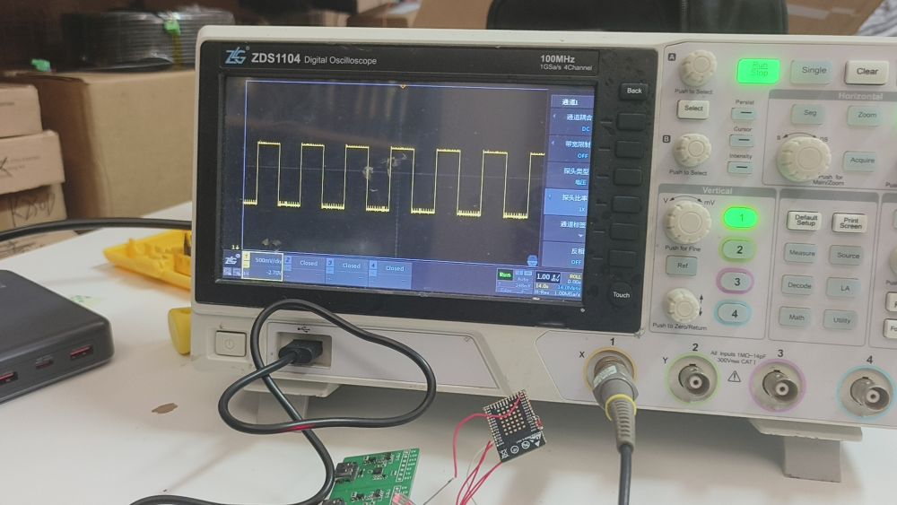
With firmware running, validation begins where software meets hardware. Every interface — I2C, SPI, UART, analog channels, and high-speed buses — is checked for clean, glitch-free communication: correct levels, stable timing, no marginal noise. Signal validation proves the board honors the interface contracts the schematic promised.
Confirm Function and Stress Performance
Functional validation walks the requirements captured at system-level analysis and proves each one holds on the real device — every user-visible feature, every control loop, every state transition. The requirement-traceability table built in stage one becomes the test matrix here, closing the loop that started at the very beginning of the process. Feature-by-feature checks are not the end: a feature that works on a bench is not a shipped product. Performance validation measures the device under realistic load, then stability validation stresses the design with temperature cycling, supply-voltage variation, humidity, and extended soak runs until statistical confidence is reached. For commercial and regulated products, validation extends further to compliance, including electromagnetic compatibility, radio emissions, safety, environmental, and accelerated-life testing.
Trace Failures Back to Their Source
When a test fails, the design's documentation — the block diagram, the schematic, the layout database, the firmware tags — becomes the map. A stability problem may trace to a component choice, a layout weakness, or a firmware race; the team finds which because each stage left a trackable record. That traceability is the difference between a repeatable process and a series of lucky attempts, and it is what lets a product converge to something reliable instead of merely something that works once.
FAQs about Hardware Development Process
Q: How long does the hardware development process take?
A simple product can go from concept to a working prototype in roughly three to six months; a complex device with custom silicon or regulatory certification can take a year or more. The schedule is most often stretched by component lead times and fabrication turnarounds rather than by the engineering effort itself.
Q: What is the most expensive stage of hardware development?
Fabrication and component sourcing usually dominate cost, because they are consumed and repeated at every design iteration. Every prototype spin is a fresh set of boards and parts, which is why catching errors in the schematic and layout is what keeps those iterations affordable.
Q: Why is component selection so important?
Because every other stage inherits the choice. A part with ideal specifications but a long lead time or a looming end-of-life forces a redesign or a schedule slip that no amount of downstream effort can undo. Supply-chain diligence in component selection protects the entire program.
Q: Can I skip simulation during schematic design?
For a trivial board, possibly. But simulation pays for itself the moment the design includes a power stage or an analog front-end, because those are the circuits whose failures are the most expensive to find later. An error caught in simulation costs minutes; the same error caught on a fabricated board costs days and money.
Q: What should I look for when choosing a PCB fabricator?
Match the fabricator's minimum trace width, clearance, and drilling capability to your design, and verify their track record for holding layer count and impedance tolerances.Don't compare quotes on price alone. Lead time, manufacturing capabilities, quality control, and consistency can have just as much impact on the final cost.
Conclusion
Turning an idea into a working product is a chain of decisions in which each stage narrows the room for the one that follows. System analysis sets the boundaries; component selection commits money and lead time; schematic, layout, and fabrication turn intent into a physical object; firmware makes it live; and validation proves it keeps its promises in the field. Hardening any single stage without the others yields a prototype, not a product — and cutting any stage early simply pushes its cost, multiplied, onto the stages downstream. For anyone moving hardware from concept to production, treating the hardware development process as a connected whole — rather than a list of independent chores — is what separates a device that ships from one that never leaves the bench.
Popular Articles
• Understanding the Basics of Electronic Devices and Circuits
• Understanding Digital Circuit Timing: Setup Time, Hold Time, Contamination Delay & Clock Skew
• PCBs Explained: A Simple Guide to Printed Circuit Boards
• Guide to the Top 10 Commonly Used Electronic Components
• Digital 101: Fundamental Building Blocks of Digital Logic Design
Keep Learning
The Hardware Development Process: From Concept to a Finished Electronic Product
Key Takeaways A structured hardware development process turns concepts into functional products through key development stages. Proper PCB design balances performance, manufacturability, and reliability. Early manufacturing considerations help reduce risks and improve prototype success. A reliable PCB partner enables smoother transitions from design to production. Every electronic device you have ever used began as a single idea. A desk lamp that brightens with a tap, a wireless earbud, a controller i......
Demystifying Bare PCB Quality for Reliability-Critical Applications
Key Takeaways Early Defect Catching: Catching faults at the bare board stage costs only the PCB, avoiding wasted components and rework later. Perfboard Risks: Zero PCBs lack reference planes and plated holes, causing signal noise above 10–20 MHz and pad lifting. Critical Material Specs: Reliability depends on hole barrel copper (20–25 µm), Tg, Td, and CTI ratings matching your operating environment. Finish & Shelf Life: HASL and ENIG last ~12 months, while OSP and Immersion Silver/Tin expire in ~6 mon......
A Comprehensive Guide to Capacitor ESR: What It Is, Good Values, and How to Measure It
Key Takeaways Definition: Capacitor ESR (equivalent series resistance) is the single resistance that represents the losses inside a real capacitor, from its electrodes, terminations, electrolyte, and dielectric. Why It Matters: Ripple current flowing through the ESR produces a ripple-voltage step on the supply rail and I²R heating in the capacitor, which limits the capacitor's ripple-current rating and service life. Conditions Matter: ESR varies with frequency, temperature, capacitance, case size, and......
Understanding IPC-6012 Standards for High-Reliability Rigid PCB Fabrication
Key Takeaways IPC-6012 vs. IPC-A-600: IPC-6012 is the binding specification, while IPC-A-600 is only for visual reference. Class 2 vs. Class 3: Class 3 requires thicker copper (25μm vs. 20μm) and zero plating voids. Coupon Verification: Quality is tested by microsectioning panel coupons after thermal stress. Upfront Callout: Specify the class on drawings upfront; boards cannot be upgraded later. IPC-6012 is the line on your fabrication drawing that decides what your supplier is allowed to ship. Most d......
Mastering PCB Plating Types and Process Control in High-Yield Fabrication
Key Takeaways Two-Step Plating: Chemical seed layer comes first, electrolytic copper adds structural strength. Process Choice: Pattern plating enables fine tracks; panel plating suits heavy copper. Via Integrity: Keep aspect ratio ≤ 10:1 to prevent thinnest-point barrel cracking. Surface Finishes: Use ENIG for flat BGA pads and hard gold for high-wear contacts. IPC Standards: Class 2 mandates 20μm copper wall thickness; Class 3 requires 25μm with zero voids. PCB plating turns a stack of drilled lamina......
Can PCB Autorouters Really Deliver Production-Ready Designs?
Key Takeaways Rules over DRC: A clean DRC only proves rules were followed, not that the board works. Placement First: Autorouters cannot compensate for bad component placement. Selective Automation: Hand-route power, analog, and high-speed traces; autoroute only repetitive or low-speed nets. DFM Validation: Verify real manufacturing tolerances before sending files to production. Every PCB autorouter sells the same promise: press one button and watch the ratlines turn into copper. On a simple two-layer......