
How to Prepare Perfect Gerber Files for Flawless PCB Production
12 min
- What Gerber Files Are and Why They Are the Language of PCB Manufacturing
- Core Components of a Complete Gerber File Set
- Common Gerber File Mistakes and How to Avoid Them
- Advanced Tips for Optimizing Gerber Files
- JLCPCB's Expertise in Gerber File Processing and Manufacturing
- FAQ about Gerber File
- Conclusion
Key Takeaways
- Use RS-274X format and consistent millimeter units for all files.
- Always include complete layers: Copper, Solder Mask, Silkscreen, Board Outline, and NC Drill.
- Check your Gerbers in a viewer before uploading to catch errors early.
- Follow DFM rules: proper annular rings, solder mask expansion, and trace spacing.
- Use clear file naming and detailed fabrication notes.
After spending weeks working on the perfect board layout, the routing is clean, the DRC passes, and you hit “export.” Two days later, your fabricator calls back and asks, "Why don't you have a layer for your solder mask, and why did your drill file use inches instead of millimeters for your copper layer? Sound familiar? The problem with almost all these problems is that in the end, they all boil down to one thing: the Gerber file. A Gerber file, the one critical deliverable that you provide a PCB manufacturer, is the one that many engineers consider as an afterthought.
If you get it right, your boards will arrive exactly as you designed! If you get it wrong, you're going to face delays, remakes, or worse, boards that look fine, but won't work. In this guide, I'm going to explain to you what a Gerber file is, the layers that comprise a full set, the things that quietly kill production runs, and the advanced habits that can make for a pleasant or unpleasant handoff. At the end, you will be well informed as to how to prepare files that make it through manufacturing the first time.
What Gerber Files Are and Why They Are the Language of PCB Manufacturing
Definition and Role in the Fabrication Process
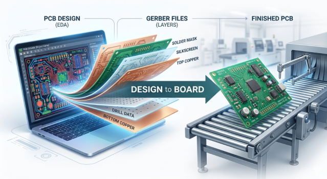
A vector-based 2D image file that describes one layer of your PCB, with a standardized format, is a Gerber file. Consider it to be a blueprint of sorts that tells the manufacturing equipment where to lay down copper, where to cut open the solder mask, and where to put the silkscreen. Every layer of your physical board will be represented by one Gerber file, and all of the Gerbers together will describe your board.
The format is officially known as RS-274X, which is also known as Extended Gerber, and the modern revision is Gerber X2 with added attribute information such as netlist, layer function, etc. So if you're asked "what is a Gerber file", the easiest answer is this: Gerber is the universal language to communicate your EDA design to a fabrication line so that they can actually fabricate your design.
The Evolution from Hand-Taped Designs to Digital Gerber Standards
People can easily forget that the PCBs were hand-laid. Engineers affixed black tape and adhesive pads to clear film in 2x or 4x size and subsequently shot to size to produce artwork for production. The Gerber format was originally designed to control photoplotters, which used to flash a light through an aperture wheel to expose film (hence the term "aperture"), and that's why we still use the term aperture today.
The original format was RS-274D, and it used a separate aperture list file to specify shapes – when this was lost, there was a lot of confusion. The move to embedded aperture definitions in the file removed a whole class of errors in the leap to RS-274X. Today's PCB Gerber file format has been built up over decades. The original concept has been extended to modern Gerber X2, ODB++, and IPC-2581 formats, which also include intelligent data, but the basic idea is the same: one file per layer, clean and unambiguous.
Core Components of a Complete Gerber File Set
Essential Layers (Copper, Solder Mask, Silkscreen, Drill, etc.)
Each full Gerber set is made up of a known set of layers. With a standard two-layer board, you can expect the following:
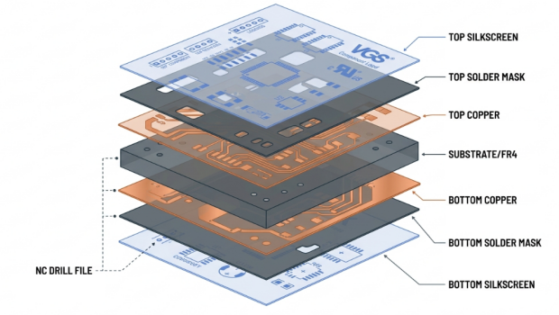
- Top and Bottom Copper: This is the conductive traces, pads, and pours that deliver your signals and power.
- Top (or Bottom) Solder Mask: Specifies where to remove the green (or other color) mask to reveal the pads for solder.
- Top and Bottom Silkscreen: The white printed-out text, reference designators, and outlines.
- Top and Bottom Solder Paste: It is not included in the bare board, but solder paste is required to make the stencil for SMT assembly.
- Board Outline / Mechanical: The physical outline that will instruct the router where to cut.
Multilayer boards are simply the addition of the inner copper layers in their proper order of stackup. A four-layer board, for instance, will have two extra inner copper sheets located between the outer two. One thing that people don't understand: solder mask is a negative layer. Any mask that is drawn is removed where the feature is drawn. This is the inverse of how copper works, and often is a source of exposed copper or covered pads.
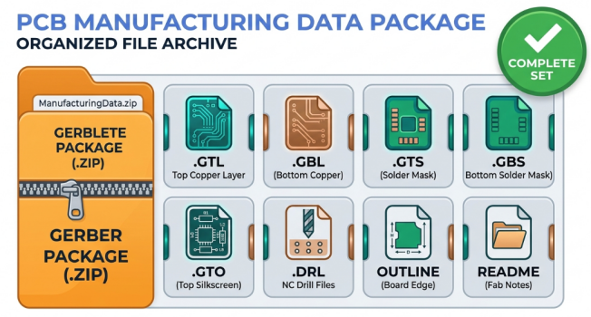
Supporting Files (NC Drill, README, Netlist)
Gerbers are for imaging layers; holes are a different animal. A separate NC Drill file, typically in Excellon format, is used for drilling, containing each hole's coordinate and diameter, and whether it is plated or non-plated (PTH or NPTH). A professional handoff consists of a few supporting documents in addition to the drill file:
- Excellon NC Drill file: Hole positions, sizes, and plating type.
- Drill drawing or map: A human-readable reference showing hole symbols.
- Netlist file (IPC-D-356): lets the fab run electrical comparison testing against your intended connections.
The netlist is of special mention. If you're including an IPC-D-356 netlist, the fabricator will not only know whether the boards are manufactured to your required connectivity, but also if any shorts or opens will occur in the manufactured copper, before the boards even leave the fabricator's doors.
Common Gerber File Mistakes and How to Avoid Them
Incorrect Aperture Lists, Scaling Errors, and Missing Layers
The worst errors have a common theme: Data is self-inconsistent. Let's check out the common suspects.
- Scaling and unit mismatches: When exporting copper in millimeters and a drill file in inches, it is bound to be the wrong size or with misplaced holes on the board.
- Missing layers: The most frequent cause for a fab to stall your order is missing layers (solder mask or board outline).
- Legacy aperture problems: When exporting old RS-274D exports, you might lose the aperture file. This all can be solved by exporting RS-274X.
- Not enough coordinate precision: Not enough decimal places to round to the correct position of fine features; important on high-density designs.
All of these are easily cured and cost nothing: Just check your output with a Gerber file viewer before uploading it. A good Gerber file viewer will display all the layers exactly as the fab will view them. If you see it on the computer, it is wrong, and you just spared yourself a remake.
Best Practices for File Naming and Organization
Naming is not some kind of aesthetics, but it will have a direct impact on whether a CAM engineer will map your layers properly. Names like "layer1.gbr" are sloppy and prone to errors from guessing mistakes. Practice some basic habits:
- Descriptive extensions or suffixes to indicate the layer function, like.GTL (top copper).GBL (bottom copper), GTS (top solder mask), and .GTO (top silkscreen).
- Put all the sets into one folder and zip them all up to upload.
- Avoid combining multiple design versions in a folder.
- Attach your fab notes file with the same base name as your job so that it is easy to see what it is for.
Advanced Tips for Optimizing Gerber Files
Design for Manufacturability (DFM) Considerations
Design for Manufacturability (DFM) is the concept of designing something around what can be built reliably at the factory, not necessarily what your software will allow you to draw. Your Gerbers will have this information, and the geometry must adhere to actual process limits. Here are some DFM considerations to bear in mind prior to exporting:
- Do not go below the minimum (fab) trace width and spacing, as this will lead to shorts and opens.
- Have sufficient annular ring around drilled pads for holes to remain centered in copper. Make sure solder mask slivers between fine pitch pads are not thin enough to come off during the process.
Standards like IPC-2221 (generic design) or IPC-A-600 (board acceptability classes) provide specific goals. Design to at least IPC Class 2 is a safe design within the range of most prototype and mid-volume fabs.
Preparing Files for High-Precision and Complex Boards
The Gerber package has to work harder when your board ventures into HDI, controlled impedance, or fine-pitch BGA applications. Precision and documentation are a must. To do so, you should specify your state impedance requirements in your fab notes: whether nets are 50 ohm single-ended or 90 ohm differential/100 ohm single-ended, etc., and adjust the stackup geometry accordingly. Coordinate resolution should be adequate (4.6 format in millimeters) for microvia and fine-pitch accuracy. It's important to distinguish between plated and non-plated holes in your drill data. Finally, for the most demanding tasks, try out IPC-2581 or ODB++; these formats combine stackup, netlist, and drill data in a single package, reducing back-and-forth.
JLCPCB's Expertise in Gerber File Processing and Manufacturing
Automated Gerber Analysis and Instant DFM Feedback
After your ZIP is uploaded to JLCPCB, your Gerber and drill files are almost instantly processed and converted to an online viewer. You will be able to see your board as the factory does, layer by layer, before making any decision. The platform performs automated DFM checks as part of its process capabilities and alerts to any features that may need to be adjusted, such as undersized traces, tight clearances, etc., right in the quoting flow, even missing board outline. But detecting the problem at upload time means one day less delay versus a manufacturing hold that could last for days.
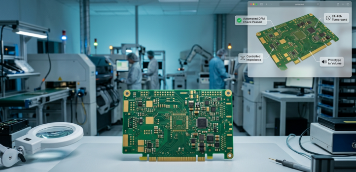
Precision Fabrication with Strict Process Controls
The key to a clean Gerber is to maintain tight tolerances, and JLCPCB is serious about process control. The fabrication line allows for fine trace and space rules, controlled impedance stack-ups, and the full range of surface finishes, including HASL, lead-free HASL, and ENIG. That precision means the copper geometry that you specify in your Gerber will be exactly what you see when you receive the board. If your file is a 0.1 mm trace, then you will receive a 0.1 mm trace, with the registration and etch control to ensure reliable dense designs.
FAQ about Gerber File
Q: What is a Gerber file in simple terms?
A Gerber file is a standard 2D vector file that describes one layer of a PCB, telling the manufacturing equipment exactly where to place copper, solder mask, or silkscreen. A complete board is described by a set of these files plus a separate drill file. It is the universal language nearly every PCB fabricator uses to build your design.
Q: What files do I need to send besides the Gerbers?
At a minimum, you need an Excellon NC drill file alongside your imaging Gerbers. For a smoother handoff, also include a drill map, an IPC-D-356 netlist for electrical verification, and a README with board thickness, copper weight, surface finish, and any impedance requirements.
Q: How do I check my Gerber files before uploading?
Open the full set in a dedicated Gerber file viewer and review each layer the way the fabricator will see it. Confirm that all layers are present, units and scaling match between copper and drill data, and the board outline is closed. Many manufacturers, including JLCPCB, also render your files in an online viewer during quoting.
Q: What is the difference between the RS-274D and RS-274X Gerber formats?
RS-274D stored aperture definitions in a separate file, which often went missing and caused errors. RS-274X (Extended Gerber) embeds those aperture definitions directly inside each file, making it self-contained and far more reliable, and it is the format you should always use today.
Conclusion
A Gerber file isn't the last-minute paperwork you create; it's a contract between your design and what ends up on your desk in a physical board. Once the layers are done, the units are consistent, the drill data is clean, and the fab notes are clear, manufacturing is almost boringly predictable, which is what you want. The behaviors you need to do to get there are not overly complex. Make sure to export the entire layer set, preview in a Gerber file viewer, use the Gerber X2 file format, name Gerber files, and document special requirements. Combine those good habits with a manufacturer like JLCPCB that automates the analysis and makes sure it's fabricated correctly, and you have the very best chance of getting your boards right the first time. Take care in preparing the file, and the remainder of the process generally follows naturally.
Keep Learning
How Beveled Edges Improve Reliability and Performance in Card Edge Connectors
Key Takeaways Beveled edges enable smooth insertion and protect gold fingers from wear in card edge connectors. Use 30° or 45° angles (45° is standard for most designs) with depth of 1/3 to 1/2 board thickness. They reduce insertion force, prevent plating damage, and improve long-term contact reliability. Proper beveling is critical for high-cycle applications like DDR modules and PCIe cards. Bevel edges came into my attention the first time a memory module that I designed scratched its own gold finge......
How to Prepare Perfect Gerber Files for Flawless PCB Production
Key Takeaways Use RS-274X format and consistent millimeter units for all files. Always include complete layers: Copper, Solder Mask, Silkscreen, Board Outline, and NC Drill. Check your Gerbers in a viewer before uploading to catch errors early. Follow DFM rules: proper annular rings, solder mask expansion, and trace spacing. Use clear file naming and detailed fabrication notes. After spending weeks working on the perfect board layout, the routing is clean, the DRC passes, and you hit “export.” Two day......
Technical Guidance: V-Cut Panelization Standards
For boards with regular rectangular shapes, V-cut (V-scoring) panelization is an efficient method. This process involves cutting V-shaped grooves of a specific depth on both sides of the panel along the board boundaries, leaving a thin web of material (typically about 1/3 of the board thickness) that allows easy manual separation after SMT assembly. After separation, minor thread-like fibers or rough edges may remain and can be lightly scraped off. Due to material expansion and cracking during depanel......
Technical Guidance: Character Design Specifications
To facilitate component assembly, future maintenance, and traceability of PCB manufacturing information (such as manufacturer, production date, batch number, etc.), various character markings are typically silk-screened onto the PCB. These include component designators, polarity marks, test point labels, company logos, and production traceability information. Traditional PCB character silk-screening uses the screen printing process, hence the term “silk-screen characters.” High-definition characters a......
Technical Guidance: Mouse Bite Panelization Guide
The conventional method of panelization uses V-grooves. However, for irregularly-shaped boards or special requirements (such as JLCPCB's economic SMT assembly), mouse bite panelization, which resembles postage stamps on an envelope, is required. PCBs panelized using this method are called "mouse bite panels" or "mouse bite connections". Mouse bite panelization can be referred to as "universal panelization." As long as there is a position to add mouse bites, boards of various shapes can be interconnect......
Smart PCB Array Design for Higher Yield and Lower Production Costs
Key Takeaways Smart PCB array design is a critical strategy for achieving higher manufacturing yield and significantly lower production costs. By optimizing panelization with proper board spacing, V-scoring, tab routing, and mouse bites, designers can dramatically improve material utilization by 20-30%, enhance production throughput, and simplify handling and depaneling while minimizing mechanical stress and defects. Effective use of fiducials and careful component clearance further ensures high-quali......