The Ultimate Guide to OSP Surface Finish in PCB Manufacturing: Advantages, Process, and Selection
20 min
- 1. Why Do PCBs Need Surface Finishing in PCB Manufacturing?
- 2. How OSP Works: Chemical Principle and Process Workflow
- 3. Key Technical Advantages of OSP Surface Finish
- 4. Comprehensive Comparison: OSP vs. HASL vs. ENIG
- 5. Limitations of OSP and Selection Recommendations
- 6. Partner with JLCPCB: Precision OSP Process Control and Manufacturing Reliability
- FAQ about OSP Surface Finish in PCB Manufacturing
- Conclusion on OSP Surface Finish
Key Takeaways
OSP (Organic Solderability Preservative) is a water-based, cost-effective PCB surface finish that deposits a 0.2-0.5μm organic film directly onto copper pads. Unlike metallic finishes such as ENIG or HASL, OSP provides superior surface flatness for fine-pitch SMT components at no extra process charge, making it ideal for high-density consumer electronics. However, OSP requires controlled handling and a limited assembly window (24-48 hours after opening vacuum packaging). It is best suited for fine-pitch BGA/QFN designs with standard double-sided SMT processing, but unsuitable for edge connectors, castellated hole modules, or military-grade hardware.
1. Why Do PCBs Need Surface Finishing in PCB Manufacturing?
1.1 The Vulnerability of Bare Copper to Oxidation and Contamination
Bare copper traces on a printed circuit board rapidly oxidize when exposed to ambient atmospheric oxygen and humidity, generating an insulating layer of copper oxide. This oxide barrier degrades solderability, prevents solder flux wetting, and leads to defective intermetallic compound (IMC) formation during SMT assembly. Therefore, exposed copper pads require protective surface finishes to maintain long-term solderability.
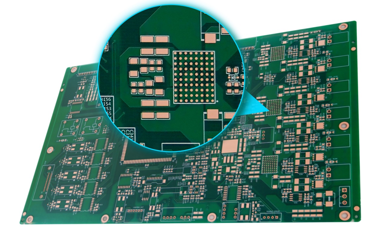
In raw printed circuit board fabrication, copper is the primary metal used for traces and pads due to its exceptional electrical and thermal conductivity. However, untreated copper is chemically active. Upon exposure to ambient air, bare copper undergoes an exothermic oxidation reaction, forming copper(I) oxide (Cu2O) and copper(II) oxide (CuO) within hours.
These surface oxide films act as physical and electrical insulators. During automated Surface Mount Technology (SMT) assembly, solder paste flux must clean the metal surfaces to allow molten tin alloy to react directly with solid copper. When oxidation is severe, standard organic flux cannot fully dissolve the oxide crust within the narrow time-temperature window of a reflow oven. This results in high wetting angles, incomplete solder coverage, dewetting, or complete solder joint failure. Furthermore, atmospheric contaminants such as airborne sulfides, chlorides, and human skin oils exacerbate surface degradation, necessitating an immediate protective barrier upon copper pattern etching.
1.2 Core Functions of Surface Finish: Protection and Solderability
A PCB surface finish serves two vital engineering functions: preventing copper pad oxidation during storage and providing a clean metallurgical interface for solder joint formation during assembly. By keeping pad surfaces pristine, the surface finish ensures molten solder spreads uniformly to create robust intermetallic bonds. Choosing the correct finish directly dictates manufacturing yield, pad coplanarity, and product reliability.

The primary objective of any surface finish is to bridge the time gap between bare board fabrication and SMT component assembly. From a metallurgical perspective, a surface finish does not merely act as a temporary coat; it dictates the interfacial reactions during soldering. When molten solder (such as SAC305 or SnPb) contacts a protected copper pad, the flux cleans away the protective coating or oxide residues. The liquid tin then dissolves a microscopic layer of copper to form an intermetallic layer—primarily Cu6Sn5 (η-phase) at the interface, which later transitions into Cu3Sn (ε-phase) after thermal aging.
Without an effective surface finish, this intermetallic reaction is hindered, yielding weak mechanical bonds subject to fatigue failure. Additionally, modern high-density interconnect (HDI) designs feature sub-100μm traces, fine-pitch Ball Grid Arrays (BGAs), and Quad Flat No-lead (QFN) packages. These components demand flat pad surfaces. The selected surface finish dictates surface coplanarity, shelf life durability, in-circuit testing (ICT) probe contact quality, and resistance to multiple thermal reflow cycles.
2. How OSP Works: Chemical Principle and Process Workflow
2.1 The Chemical Reaction Behind Azole-Based Organic Films
An OSP surface finish relies on a chemical reaction between bare copper and organometallic compounds—typically alkylbenzimidazoles—to yield a thin, protective coating. This self-limiting reaction deposits a uniform organic film between 0.2μm and 0.5μm thick directly onto the copper pads. The resulting transparent film acts as an oxidation barrier under ambient storage conditions while retaining the pad's natural copper color.
Unlike metallic plating techniques such as ENIG (Electroless Nickel Immersion Gold) or HASL (Hot Air Solder Leveling), Organic Solderability Preservatives (OSP) deposit a non-metallic organic layer. The process utilizes azole-based chemistry, where nitrogen atoms in the alkylbenzimidazole ring share lone pairs of electrons with surface copper ions (Cu+ or Cu2+). This forms an insoluble organometallic coordination polymer film.

Because the reaction requires direct contact between the active chemical solution and bare copper, the film growth slows down automatically once the copper surface is completely sealed. This self-limiting property caps the film thickness at 0.2-0.5μm (200 to 500 nanometers). The film selectively adheres to copper surfaces, leaving the surrounding epoxy glass laminate and solder mask untouched.
2.2 Step-by-Step OSP Chemical Processing Workflow
Applying an OSP surface finish involves an automated, multi-stage chemical conveyor process comprising degreasing, surface micro-etching, OSP bath immersion, and thermal drying. Precise control over chemical bath temperature, pH, and line speed is essential to maintain uniform coating thickness. Modern PCB manufacturers utilize specialized horizontal or vertical conveyor lines to ensure process repeatability.
-
Degreasing & Cleaning
The bare copper PCB passes through an alkaline or acidic degreaser to remove organic oils, finger marks, and surface oxides. This step ensures uniform chemical wet-out across all pads.
-
Micro-Etching
The board enters a sodium persulfate or hydrogen peroxide/sulfuric acid micro-etching solution. This removes approximately 1.0-1.5μm of copper, creating a micro-roughened surface topography that increases surface area and enhances OSP film adhesion.
-
Acid Rinse & Activation
An acid rinse removes micro-etch residues and lowers the pH of the copper surface, preparing it for organometallic bonding.
-
OSP Coating (Application Bath)
The PCB is immersed in or sprayed with the active OSP bath maintained at 25℃-40℃ for 30 to 120 seconds. Chemical parameters (pH, concentration, temperature) are monitored to achieve the target thickness (0.2-0.5μm).
-
Deionized (DI) Water Rinse
Deionized water washes away unreacted chemical solution and drag-out residues to prevent staining or ionic contamination.
-
Hot Air Drying
The PCB is dried using clean, heated forced air (60℃-80℃). Rapid drying sets the organic film, yielding a smooth, transparent, light pink/copper-toned pad finish.
2.3 The Degradation and Removal of OSP Film During SMT Reflow
During the SMT reflow process, the protective OSP film breaks down under high temperatures and active solder paste flux, exposing raw copper to liquid solder. The acidic flux components chemically dissolve the organometallic polymer layer while thermal heat weakens its bond matrix. This allows tin-based solder alloys to wet the copper pad directly and form clean intermetallic joints.
The core advantage of an OSP surface finish lies in its transient nature: it protects copper pads during ambient storage but disappears during soldering. When the PCB enters the SMT reflow oven, solder paste deposited via stencil printing covers the pads. As temperature rises within the preheat and soak zones (150℃-200℃), organic acids (such as rosin or carboxylic acids) inside the solder flux activate.
These flux acids break the copper-nitrogen coordination bonds within the alkylbenzimidazole layer. The degraded organic compounds dissolve into the flux vehicle and float away from the joint interface. When the temperature crosses the solder liquidus point (217℃ for SAC305, 183℃ for SnPb), molten solder makes direct contact with oxide-free copper, establishing a reliable metallurgical interface without leaving organic inclusions inside the solder joint.
3. Key Technical Advantages of OSP Surface Finish
3.1 Superior Surface Flatness for Fine-Pitch SMT Components
An OSP surface finish yields excellent pad coplanarity because the sub-micron film (0.2-0.5μm) conforms directly to the flat copper topology without adding metallic volume. This planarity eliminates height variations, drastically reducing assembly defects such as solder bridging or tombstoning on fine-pitch components. Consequently, OSP is ideal for high-density SMT designs featuring BGA, QFN, and 0201/01005 packages.
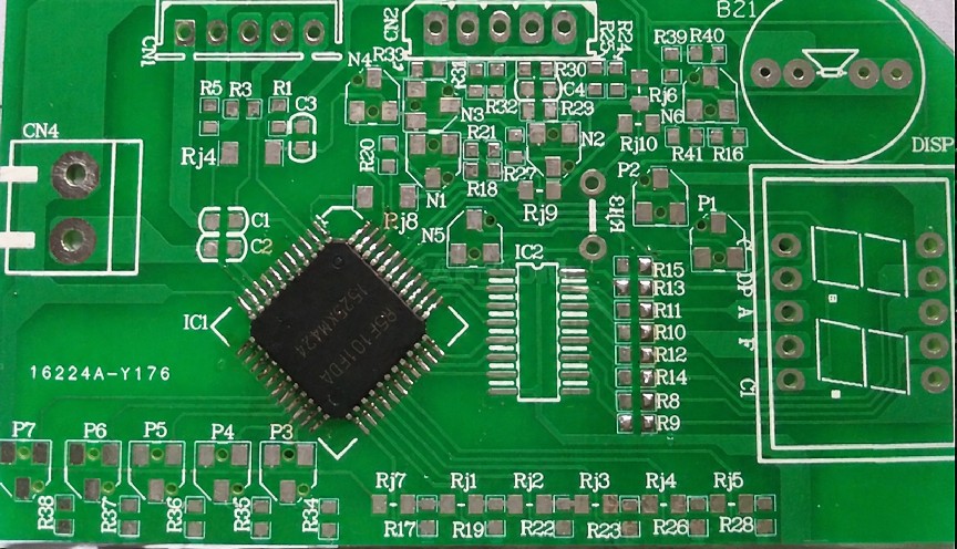
In modern electronics, surface coplanarity is critical for high SMT yield. Traditional Hot Air Solder Leveling (HASL) leaves uneven solder domes due to air-knife pressure variations, yielding pad height differences between 1μm and 40μm. When placing fine-pitch BGAs with 0.4mm ball pitch or ultra-small 0201/01005 passive components onto HASL pads, component tilting, open joints, and bridging frequently occur.
Because OSP is applied via a controlled chemical reaction, pad height is dictated solely by the underlying copper foil etching uniformity. The surface remains completely flat across the entire panel. Solder paste printed onto OSP pads maintains uniform stencil release volume, ensuring consistent solder ball collapse on BGAs and preventing tombstoning on minute chip components.
3.2 Exceptional Cost-Efficiency in High-Volume Production
OSP provides substantial cost efficiency compared to precious metal finishes like ENIG, as it requires no expensive raw materials such as gold or palladium. The chemical application process operates at low temperatures with high throughput and low utility consumption. For high-volume consumer and industrial electronics, OSP significantly reduces PCB unit cost without compromising assembly yield.
Raw material pricing heavily influences PCB unit costs in high-volume manufacturing. ENIG finishes require electroless nickel and immersion gold plating baths, making them susceptible to global gold market price fluctuations. In contrast, OSP chemistry utilizes cost-effective organic azole compounds and dilute acids.
At major fabricators like JLCPCB, selecting OSP introduces zero extra process premiums over standard base panel manufacturing. This contrast becomes stark on large multi-layer panels, where ENIG charges increase proportionally with surface area. Furthermore, OSP processing lines feature shorter cycle times and fewer chemical baths than complex plating lines, reducing chemical maintenance costs and driving lower unit pricing for prototype and mass-production runs.
3.3 Simple Process Maintenance and Eco-Friendly Profile
The OSP coating process is environmentally friendly and compliant with RoHS and REACH standards due to its complete absence of lead or toxic heavy metals. The water-based chemical bath operates at moderate temperatures (25℃-40℃) with lower chemical complexity than electroless plating lines. This simplifies wastewater treatment and reduces the carbon footprint for PCB fabricators.
Environmental compliance is mandatory in modern electronics manufacturing. Traditional SnPb HASL processes contain up to 37% lead, failing RoHS compliance. While Lead-Free HASL eliminates lead, it requires high processing temperatures (260℃-270℃), imposing significant thermal stress on FR-4 laminates and consuming substantial energy.
The OSP process operates at near-ambient temperatures (25℃-40℃) and uses aqueous chemistry free of heavy metals, cyanides, or toxic chelating agents. Wastewater treatment involves straightforward neutralization and organic filtration, making OSP one of the most eco-friendly surface finishing options available in the circuit board industry.
4. Comprehensive Comparison: OSP vs. HASL vs. ENIG
4.1 OSP vs. Lead-Free HASL: Flatness vs. Shelf Life
While Lead-Free HASL offers extended shelf life, it creates an uneven solder coating (1-40μm) that causes coplanarity issues on fine-pitch pads. In contrast, OSP provides flat pad surfaces ideal for advanced SMT packaging, though it requires stricter handling and ambient storage controls. For modern multi-layer boards, OSP outperforms Lead-Free HASL in fine-pitch assembly yield.
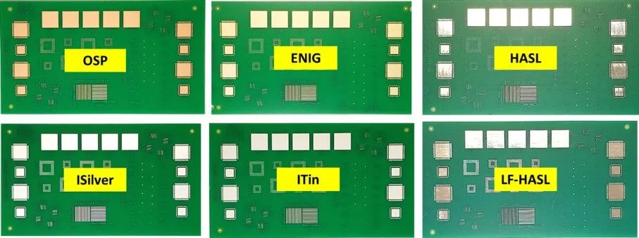
Lead-Free HASL leaves a pre-deposited tin-alloy layer on pads, offering resistance to environmental storage degradation. However, the thermal shock of plunging boards into a molten solder bath at 260℃ can cause board warp, Z-axis expansion, and micro-cracking in plated through-holes (PTH).
OSP avoids thermal shock entirely during board fabrication. For high-density board fabrication, leading manufacturers like JLCPCB have phased out HASL on 6-layer and higher advanced HDI boards, adopting OSP and ENIG as standard offerings to meet tight geometric tolerances.
4.2 OSP vs. ENIG: Cost-Effectiveness vs. Multiple Reflow Cycles
ENIG offers strong corrosion resistance and long storage durability, but carries material cost premiums and risks of "black pad" nickel defects. OSP delivers equivalent surface flatness at a lower cost without nickel-intermetallic failure modes, though ENIG performs better under multiple thermal reflow passes. Engineering decisions balance budget constraints against required thermal cycle robustness.
ENIG deposits 3-6μm of electroless nickel followed by 1-2μ" (0.025-0.05μm) of immersion gold. Gold provides an inert protective layer, while nickel acts as a diffusion barrier. However, hyper-corrosion of the nickel layer during immersion gold displacement can cause "black pad" defects—a brittle nickel-phosphorus layer that leads to catastrophic solder joint failure under impact.
OSP eliminates black pad risks entirely because solder bonds directly to copper. While OSP is sensitive to multiple thermal reflow passes—as heat degrades un-soldered organic films—proper flux selection enables standard double-sided SMT processing (withstanding up to 2 reflows and 2 wave solder passes) at a fraction of ENIG's cost.
4.3 Visual and Technical Comparison Matrix of PCB Finishes
The engineering selection of a PCB surface finish requires balancing coplanarity, cost, storage lifespan, soldering robustness, and application constraints. Visual inspection highlights distinct cosmetic differences: OSP maintains natural copper tones, ENIG presents a golden luster, and HASL shows silver-gray solder coating. The technical comparison matrix below summarizes key operating parameters across primary industry surface finishes.
| Process Parameter | HASL (Leaded) | Lead-Free HASL | ENIG | OSP Finish |
|---|---|---|---|---|
| Primary Material | Sn63/Pb37 Alloy | Lead-free Sn alloy (<0.5% Pb) | Ni: 3-6 μm, Au: 0.025-0.05 μm | Organometallic Polymer Film |
| Layer Thickness | 1-40μm | 1-40μm | 3-6μm (Ni) | 0.2-0.5μm |
| Surface Flatness | Poor (Uneven solder dome) | Poor (Uneven solder dome) | Excellent (Flat deposition) | Superior (Conformal flat copper) |
| Relative Cost | Lowest | Low | High (Subject to gold price) | Very Low (No extra fee at JLCPCB) |
| RoHS Compliant | No (Lead up to 37%) | Yes | Yes | Yes |
| Nominal Shelf Life | 12 Months | 12 Months | 12+ Months | ~3 Months (Unopened vacuum) |
| Thermal Robustness | High | High (Thermal stress risk) | Excellent | Up to 4 passes (2 Reflow/2 Wave) |
| BGA / Fine Pitch | Not Recommended | Not Recommended | Ideal | Ideal |
| Gold Fingers / Plug | Unsuitable | Unsuitable | Ideal | Unsuitable (Lacks wear resistance) |
5. Limitations of OSP and Selection Recommendations
5.1 Technical Limitations: Short Storage Window and Handling Sensitivity
OSP coatings are physically delicate and sensitive to handling, requiring gloves during assembly to prevent hand oils from breaking down the organic film. Unpacked OSP boards feature a limited assembly window, typically requiring SMT processing within 24 to 48 hours after opening. Unopened boards generally maintain a shelf life of approximately 3 months under standard ambient storage conditions.
Despite its process advantages, OSP imposes operational constraints during handling and storage:
OSP Handling Constraints
Handling Sensitivity: Direct touch with bare fingers transfers skin acids, sodium salts, and oils onto the pad. These contaminants dissolve the nanometer-thin OSP film, causing rapid copper oxidation prior to solder paste printing. Operators must wear clean ESD nitrile gloves at all times.
Storage Environment: Unopened vacuum bags must be stored under controlled environmental conditions (20℃-25℃, Relative Humidity < 60%). The nominal shelf life for unopened boards is 3 months.
SMT Floor Life Window: Once the vacuum bag is opened, the boards must complete double-sided SMT reflow within 24 to 48 hours. Extended exposure to atmospheric humidity degrades the un-soldered organic coating.
5.2 Multiple Reflow and Secondary Solderability Constraints
Thermal degradation of the organic film during initial reflow cycles reduces oxidation protection on un-soldered pads during subsequent passes. While high-grade OSP boards withstand up to 4 thermal cycles (typically 2 reflows and 2 wave solders), secondary solderability degrades compared to ENIG. Furthermore, non-conductive OSP films create contact resistance during In-Circuit Testing (ICT) on un-fluxed test points.
When a double-sided OSP board undergoes its first SMT reflow pass, un-printed secondary side pads pass through peak temperatures ($240^\circ\text{C}\text{--}260^\circ\text{C}$) in air or nitrogen atmospheres. This heat exposure oxidizes the OSP polymer matrix. While top-tier OSP chemistry supports up to 4 total thermal cycles (such as 2 reflow and 2 wave soldering passes), the secondary side requires higher flux activity to fully clean the pads.
A secondary challenge involves In-Circuit Testing (ICT). Because the OSP coating is electrically insulating, test probes cannot achieve low-resistance contact on un-soldered test vias or pads unless flux has dissolved the film or aggressive crown-point probes pierce the organic coating.
5.3 Practical Selection Guide: When to Choose OSP?
Selecting an OSP surface finish is optimal for high-density, cost-sensitive electronics featuring fine-pitch BGA or QFN packages subjected to standard double-sided SMT. Conversely, OSP should be avoided for sliding contacts (gold fingers), castellated hole modules with delayed secondary assembly, or military hardware requiring leaded alloys. Engineers must align component footprints, storage workflows, and mechanical contact demands.
1Preferred Applications for OSP
- High-Density HDI & Fine-Pitch SMT: Smartphones, wearable tech, tablet motherboards, and IoT modules utilizing 0.4mm pitch BGAs, QFNs, and 0201 passives where pad flatness is mandatory.
- Cost-Sensitive Mass Production: Consumer electronics, smart home devices, and automotive infotainment where minimizing BOM cost is critical.
- High-Layer Server & Router Backplanes: 10+ layer high-speed backplanes where avoiding HASL thermal shock prevents z-axis dielectric damage.
Unsuitable Applications for OSP
- Edge Connectors (Gold Fingers): PCI-e slots or plug-in cards requiring wear-resistant, high-conductivity metallic gold contacts.
- Castellated Hole Modules (Half-Holes): Daughterboards or wireless stamp modules where edge half-vias undergo manual secondary hand-soldering long after production.
- Military & Aerospace Systems: High-reliability hardware mandated by defense specs to use leaded alloys or permanent noble metal barriers.
6. Partner with JLCPCB: Precision OSP Process Control and Manufacturing Reliability
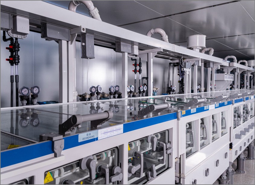
6.1 Standardized Automated OSP Production Lines at JLCPCB
JLCPCB operates fully automated horizontal OSP processing lines with computerized monitoring of chemical bath temperatures, micro-etch rates, and concentration metrics. By maintaining micro-etch rates between 1.0μm and 1.5μm and bath exposure times between 30 and 120 seconds, JLCPCB ensures consistent 0.2μm-0.5μm film coverage across production runs.
As a global PCB fabrication leader, JLCPCB utilizes automated, conveyorized OSP processing lines engineered to eliminate human error. Chemical bath parameters are tracked via closed-loop feedback systems. Micro-etching depth is verified through atomic absorption spectroscopy and weight-loss analysis to guarantee that copper pads achieve optimal surface micro-roughness without over-etching fine trace geometries.
| Processing Parameter | JLCPCB Standard Target Window |
|---|---|
| Copper Micro-Etch Removal Depth | 1-1.5μm |
| OSP Reaction Bath Temperature | 25℃-40℃ |
| Immersion / Dwell Time | 30-120 Seconds |
| Target OSP Organic Film Thickness | 0.2-0.5μm (200-500nm) |
6.2 Strict Quality Control and Moisture-Proof Vacuum Packaging
To protect OSP boards from atmospheric humidity and oxidation, JLCPCB enforces strict post-production inspection and moisture-barrier packaging protocols. Every production batch undergoes automated optical inspection (AOI) and coating thickness sampling before being vacuum-sealed with desiccant and humidity indicator cards. This guarantees boards arrive at SMT lines with pristine solderability.
Quality assurance at JLCPCB extends beyond chemical processing. Once boards clear the final hot-air drying station, they undergo 100% AOI inspection to detect surface oxidation, water spots, or copper exposure defects. Approved panels are vacuum-sealed inside anti-static ESD moisture-barrier bags containing active silica desiccant packs and humidity indicator cards. This packaging preserves board solderability throughout international transit, guaranteeing a full 3-month shelf life upon arrival.
6.3 Seamless One-Stop PCB & PCBA Assembly Services
JLCPCB integrates precision OSP board fabrication seamlessly with automated in-house SMT assembly services to deliver fast turnarounds and high manufacturing reliability. By replacing uneven HASL options on 6-layer and advanced boards with high-flatness OSP at no added finish fee, JLCPCB enables engineers to achieve high assembly yields at optimal cost.
JLCPCB simplifies hardware manufacturing by combining bare PCB fabrication and component SMT assembly under a single quality management system. Because JLCPCB's SMT lines handle thousands of OSP panels daily, reflow oven temperature profiles are optimized specifically for OSP flux dissolution dynamics.
FAQ about OSP Surface Finish in PCB Manufacturing
Q: What is OSP surface finish?
OSP (Organic Solderability Preservative) is a water-based chemical surface finish that deposits a 0.2-0.5μm thin organic film directly onto bare copper pads. It uses azole-based organometallic compounds (typically alkylbenzimidazoles) that bond with copper ions to form a transparent protective barrier against oxidation. Unlike metallic finishes, OSP is non-metallic, RoHS-compliant, and disappears during SMT soldering to expose clean copper for direct solder joint formation.
Q: How does OSP compare to ENIG?
OSP offers several advantages over ENIG including significantly lower cost (no gold or nickel), equivalent surface flatness for fine-pitch components, and elimination of black pad defects. However, ENIG provides longer shelf life (12+ months vs. 3 months), superior thermal robustness for multiple reflow cycles, and better performance for gold fingers and edge connectors. The choice depends on your budget, required storage duration, and application requirements.
Q: What is the shelf life of OSP-coated PCBs?
Unopened OSP boards in vacuum-sealed packaging with desiccant have a nominal shelf life of approximately 3 months under controlled conditions (20℃-25℃, <60% RH). Once the vacuum bag is opened, boards must complete SMT assembly within 24-48 hours to prevent oxidation of the OSP film. Always wear ESD nitrile gloves when handling OSP boards to avoid contaminating the organic coating with skin oils.
Q: Can OSP boards undergo multiple reflow cycles?
High-grade OSP chemistry supports up to 4 total thermal cycles, typically 2 reflow and 2 wave soldering passes. However, secondary-side pads require higher flux activity after the first reflow because the OSP film partially degrades during initial heat exposure. For applications requiring more than 4 thermal cycles, ENIG is recommended.
Q: Is OSP suitable for gold fingers or edge connectors?
No, OSP is unsuitable for edge connectors (gold fingers), PCI-e slots, or any application requiring wear-resistant sliding contacts. The organic film lacks the hardness and conductivity of gold plating. ENIG or hard gold plating should be specified for these applications.
Q: Does JLCPCB charge extra for OSP surface finish?
No. JLCPCB offers OSP surface finish at no additional process charge on standard PCB orders, making it an extremely cost-effective option for both prototypes and high-volume production. This contrasts with ENIG and other precious metal finishes that incur significant premiums.
Conclusion on OSP Surface Finish
OSP surface finish delivers an optimal balance of cost efficiency, surface flatness, and environmental compliance for modern high-density PCB designs. Its sub-micron organic film enables reliable fine-pitch SMT assembly at a fraction of ENIG's cost, making it the preferred choice for consumer electronics, IoT modules, and high-volume industrial applications. While its limited shelf life and handling sensitivity require process discipline during SMT operations, the benefits of zero-cost flat pad surfaces and lead-free compliance make OSP the practical default for most double-sided PCB assemblies. For engineers seeking to reduce BOM costs without compromising assembly quality, specifying OSP at JLCPCB provides a proven, cost-free path to high-yield PCB manufacturing.
Keep Learning
Choosing the Right Surface Finish for Your PCB: An Overview of HASL, ENIG, OSP, Immersion Tin and Immersion Silver
Key Takeaways Lead-Free HASL: Best low-cost, RoHS-compliant finish for general PCB builds. ENIG: Superior flatness and 12+ month shelf life for fine-pitch BGAs. OSP: Ultra-flat, lowest-cost option for high-volume SMT (3–6 month shelf life). Immersion Silver: Ideal for high-frequency RF by eliminating nickel signal loss. Immersion Tin: Best for press-fit connectors and fine-pitch assembly. Printed Circuit Boards (PCBs) are essential components in the manufacturing of electronic devices ranging from sma......
Conformal Coating in PCB Technology: Benefits, Challenges, and Future Developments
If you're searching for conformal coating, you're likely looking for a reliable way to protect your PCB from moisture, dust, chemicals, or harsh environments. Choosing the right coating directly affects product reliability, performance, and lifespan. In this guide, you'll learn what conformal coating is, the main types available, and how to select the best option for your application. We'll also cover key benefits, application methods (manual, automated, and selective), as well as inspection, rework, ......
PCB Gold Fingers: Why They Matter and How to Design Them
Key Takeaways PCB gold fingers provide reliable electrical and mechanical contact for PCBs that connect to external connectors or card slots. ENIG is suitable for general contact applications, while electroplated hard gold offers higher wear resistance for repeated insertion and removal. Gold fingers should remain fully exposed, with solder mask and silkscreen kept away from the contact area. Proper chamfering and gold finger orientation are essential to ensure smooth insertion and prevent damage duri......
Comparing HASL and ENIG Surface Finishes for PCBs
Selecting the right surface finish for a printed circuit board (PCB) is crucial to ensuring its performance, reliability, and longevity. Two of the most commonly used finishes are Hot Air Solder Leveling (HASL) and Electroless Nickel Immersion Gold (ENIG). Each of these surface finishes offers distinct advantages and disadvantages, making them suitable for different applications. In this article, we will compare HASL and ENIG to help you determine which finish is best suited for your PCB project. What......
Avoid PCB Assembly Failures: Mastering Solder Mask Expansion Rules and Best Practices
Solder mask protects copper traces and pads from oxidation, bridges, and contamination during assembly. Incorrect solder mask expansion—the clearance around features where mask is pulled back—leads to defects like shorts or exposed copper. Engineers must set expansion values precisely to ensure reliable soldering and long-term performance. Introduction: Why Solder Mask Expansion is Critical for PCB Reliability Understanding Solder Mask and Expansion Basics Solder mask is a polymer layer applied over t......
The Ultimate Guide to OSP Surface Finish in PCB Manufacturing: Advantages, Process, and Selection
Key Takeaways OSP (Organic Solderability Preservative) is a water-based, cost-effective PCB surface finish that deposits a 0.2-0.5μm organic film directly onto copper pads. Unlike metallic finishes such as ENIG or HASL, OSP provides superior surface flatness for fine-pitch SMT components at no extra process charge, making it ideal for high-density consumer electronics. However, OSP requires controlled handling and a limited assembly window (24-48 hours after opening vacuum packaging). It is best suite......