
PCB Board Outline: Smart Design Tips for Seamless Manufacturing
11 min
- What Is a PCB Board Outline and Why It Matters
- Impact on Product Fit, Mechanical Strength, and Assembly Efficiency
- Key Design Considerations for PCB Board Outline
- How Board Outline Affects Manufacturability and Panelization
- Board Outline in the Complete PCB Manufacturing Process
- FAQ about Board Outline
- Conclusion – Implementing Smart Board Outline Strategies
Key Takeaways
- Board Outline Defined: The closed polygonal contour on Mechanical Layer 1 that defines your PCB's final physical boundary, including cutouts, slots, and mounting holes.
- Why It Matters: Directly impacts enclosure fit, mechanical stability, assembly efficiency, and production yield — a well-designed outline reduces costs and lead times.
- Critical Parameters: Maintain ≥0.2 mm edge clearance, use ≥0.5–1.0 mm corner radii, and specify tolerances appropriate to your routing method (±0.1 mm precision or ±0.2 mm regular).
- Panelization Choice: V-scoring for rectangular arrays (lower cost, faster); tab routing for complex or irregular shapes (more flexible but higher cost).
- DFM Is Essential: Always run a Design Rule Check and leverage JLCPCB's online DFM checker to catch outline issues before production begins.
What Is a PCB Board Outline and Why It Matters
Clear Definition and Core Elements of Board Outline
The board outline defines the exact physical shape, dimensions, and perimeter features of your finished printed circuit board. It serves as the mechanical blueprint that guides every subsequent manufacturing step, from panelization and routing to final profiling. A thoughtfully designed board outline ensures proper enclosure fit, mechanical stability, efficient assembly, and optimal production yield.
Experienced engineers recognize that the board outline is far more than a simple rectangle — it directly impacts cost, lead time, reliability, and product integration. At JLCPCB, precise board outline processing forms a cornerstone of their manufacturing excellence, backed by advanced CNC routing equipment, rigorous DFM analysis, and extensive experience with prototypes through high-volume production.
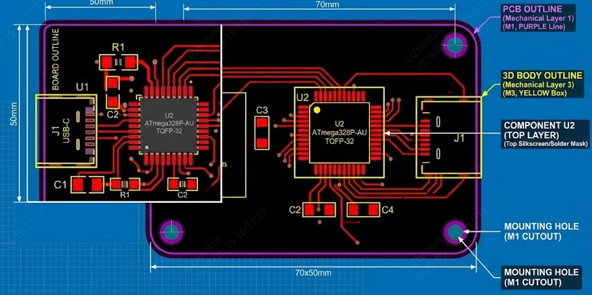
The board outline is typically drawn on Mechanical Layer 1 (often labeled GM1 or Dimension layer in Gerber output) and includes the outer perimeter, internal cutouts, slots, notches, and mounting holes. JLCPCB prioritizes the lowest-numbered mechanical layer containing a complete closed outline. Keep-out layers are ignored when a valid outline exists on a mechanical layer.
Core elements include:
- Outer contour — Must form a single, non-self-intersecting closed shape.
- Cutouts and slots — Internal features for connectors, antennas, or heat dissipation.
- Mounting holes and fiducials — Critical for mechanical assembly and automated processes.
- Line width recommendation — Approximately 0.15 mm for clear processing.
All features belonging to the final shape should reside on the same mechanical layer to avoid ambiguity. Overlapping contours default to the smaller dimension during processing. Proper definition on the correct layer prevents manufacturing errors and ensures the fabricated board matches your mechanical requirements exactly.
Impact on Product Fit, Mechanical Strength, and Assembly Efficiency
A precise board outline ensures your PCB fits perfectly within enclosures, aligns with mating connectors, and withstands mechanical stresses in the end product. Irregular shapes or inadequate corner radii create stress concentrations that may lead to cracking under vibration or thermal cycling. Proper tolerances maintain structural integrity while allowing for material expansion.
In assembly, board outline features influence automated handling. Insufficient edge clearance can cause component damage during depanelization or poor solder mask adhesion near edges. Well-designed mounting features and keep-out zones improve alignment accuracy and reduce assembly defects. For castellated edges or plated half-holes, the outline must coordinate precisely with drilling sequences. Overall, a robust board outline contributes to higher first-pass yields and more reliable end products.
Typical JLCPCB Dimension Tolerances:
| Parameter | Regular CNC Routing | Precision CNC Routing | V-Scoring |
|---|---|---|---|
| Dimension Tolerance | ±0.2 mm | ±0.1 mm | ±0.4 mm |
| Minimum Board Size | 3 × 3 mm | Same | Panel ≥70×70 mm |
| Maximum Size (FR-4 2L) | Up to 670 × 600 mm | Same | Limited by panel |
These values support a wide range of applications while maintaining high yield. Always confirm the latest specifications on jlcpcb.com during design finalization.
Common Pitfalls of Ignoring Outline Design
Common Pitfalls
- Missing or open contours cause order rejection and production delays.
- Overlapping lines or features on incorrect layers lead to unexpected board dimensions.
- Slots or cutouts on the wrong layer (or omitted from the mechanical layer) result in incomplete or unusable boards.
- Ignoring panelization early reduces material utilization and increases per-board costs, especially for complex or irregular shapes.
- Components placed too close to edges risk damage during routing and depanelization.
Engineers sometimes overlook component proximity to edges, leading to damage during routing. Early DFM consideration prevents these problems and streamlines the path from design to production.
Key Design Considerations for PCB Board Outline
Choosing Shape, Dimensions, and Precise Tolerances
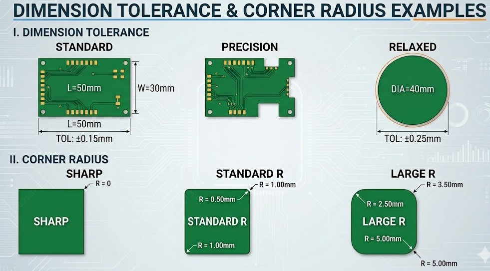
Begin board outline definition early in your CAD tool (EasyEDA, KiCad, or Altium). Rectangular boards offer the lowest cost and highest yield, but irregular polygons, rounded corners, or custom shapes suit wearables, IoT devices, or space-constrained applications. Specify realistic tolerances — JLCPCB's precision routing achieves ±0.1 mm for demanding designs, while regular routing uses ±0.2 mm.
Account for enclosure tolerances, connector protrusions, and thermal expansion. Add 0.2–0.5 mm margins where mechanical interfaces are involved. For very small boards (under 10×10 mm), consider panelization or discuss options with the manufacturer to maintain handling stability during fabrication and assembly.
Adding Cutouts, Slots, Notches, and Mounting Features
Internal cutouts accommodate connectors, switches, antennas, or thermal management components. Design all such features on the primary mechanical layer alongside the outer contour. Minimum slot width is typically 1.0 mm for non-metallized routing (matching common bit sizes). Metallized slots require coordination with drilling processes.
Mounting holes benefit from plated options with adequate annular rings (≥0.1–0.2 mm recommended). Maintain sufficient clearance (≥0.5 mm) between hole edges and nearby traces or pads to prevent shorts or mechanical weakness. Notches and chamfers can ease assembly or improve aesthetics but require careful radius specification.
Practical recommendations:
- Use arcs for internal corners with radii ≥0.5–1.0 mm to match router capabilities and reduce stress.
- Avoid extremely narrow slots that risk bit breakage or incomplete cleaning.
- Label non-plated vs. plated features clearly in your design.
Edge Clearance, Keep-Out Zones, and Component Optimization
Maintain adequate clearance from the board outline to copper features and components — JLCPCB recommends at least 0.2 mm for routed edges, though 0.3–0.5 mm or more provides a safer margin for high-reliability designs. This prevents damage during profiling and improves edge quality for solder mask and silkscreen.
Define keep-out zones around mounting areas, edge connectors, and high-stress regions. Lock critical components (heavy connectors, crystals, or antennas) relative to the outline early in layout to maintain alignment across revisions. Optimize placement to balance signal integrity, thermal performance, and mechanical constraints.
Best Practices in CAD Tools and File Output (Gerber & DXF)
Draw a single closed, continuous contour on Mechanical Layer 1 with consistent line width. Export Gerbers with the outline clearly assigned to GKO/GM1. For highly complex mechanical definitions, supplement with DXF files. Always run a full Design Rule Check (DRC) and view exported files in a professional Gerber viewer before submission.
JLCPCB's online uploader and DFM checker provide instant feedback on outline integrity, helping catch issues before production begins.
How Board Outline Affects Manufacturability and Panelization
Influence on Fabrication Yield and Production Efficiency
Board outline complexity directly affects routing time, material utilization, and overall yield. Simple rectangular outlines maximize panel density (often exceeding 90% utilization in optimized arrays). Multiple internal cutouts or highly irregular perimeters increase CNC routing time and scrap rates. JLCPCB's automated panelization algorithms analyze your outline to suggest efficient arrangements while respecting design constraints.
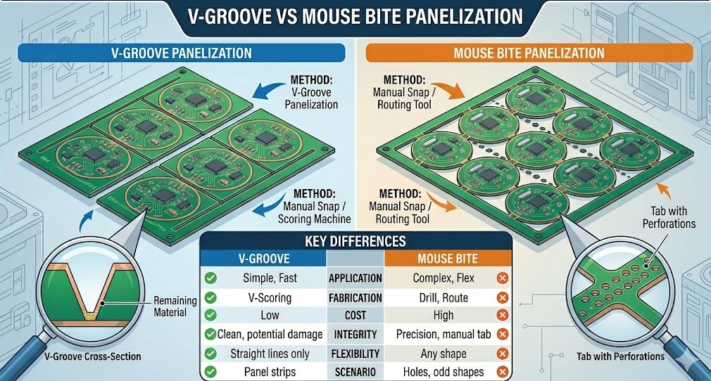
Effective Panelization Methods: V-Scoring vs Tab Routing
V-scoring creates angled grooves (typically 25° at JLCPCB) along straight lines, leaving a thin web for manual or roller separation. It is cost-effective and fast for rectangular arrays but limited to straight horizontal/vertical lines. Minimum panel size is 70×70 mm, and it works best with adequate component edge clearance (≥0.4 mm from V-cut centerline, with 3–5 mm connecting edge depending on thickness).
Tab routing (with mouse-bite perforations or solid tabs) provides maximum flexibility for irregular board outlines, curved edges, or mixed designs on one panel. Tabs maintain stability during assembly but require post-separation cleanup.
Comparison Table:
| Method | Best For | Edge Quality | Cost & Speed | Key Limitations |
|---|---|---|---|---|
| V-Scoring | Rectangular arrays | Clean break | Lower, faster | Straight lines only; edge clearance needed |
| Tab Routing | Complex/irregular shapes | Routed finish | Higher | More post-processing; tab design critical |
Critical Factors – Corner Radii, Tolerances, and Material Compatibility
Internal corner radii should equal or exceed the routing bit diameter (commonly 0.5–1.0 mm minimum). FR-4 is the most forgiving standard material, while flex, rigid-flex, or metal-core boards impose additional outline constraints. Tighter tolerances (±0.1 mm) are achievable but may influence lead time. Always align material choice with mechanical and thermal requirements of the final product.
Board Outline in the Complete PCB Manufacturing Process
-
File Preparation to Imaging, Etching, and Lamination
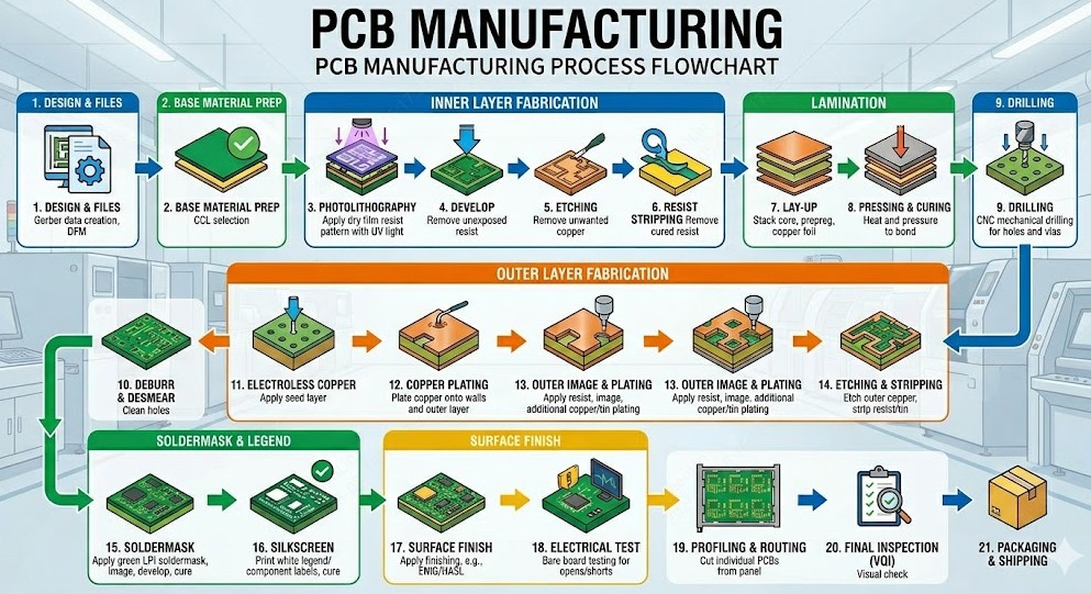
After upload, JLCPCB performs automated and manual DFM review focusing on outline integrity. Validated files guide panel setup. Inner layers undergo imaging, UV exposure, and etching. The board outline data remains a constant reference throughout lamination, where prepreg and copper foils are bonded under heat and pressure.
-
Precision Drilling, Plating, and Outline Routing
High-speed CNC drills create vias and component holes with excellent accuracy. Through-hole plating follows to establish interlayer connections. Final profiling uses precision CNC routers to follow your board outline exactly, delivering clean edges within specified tolerances. This step transforms the panel into individual boards.
-
Surface Finish Selection and Edge Quality Control
Surface finishes such as ENIG, HASL, or OSP protect copper and influence solderability. ENIG offers superior edge protection and flatness for fine-pitch or high-reliability applications. JLCPCB performs comprehensive final inspections, including edge quality, to ensure boards meet dimensional and cosmetic standards.
-
Assembly Compatibility with Outline Features
Board outline design affects SMT and THT processes. Castellated edges require half-drilled holes before final routing. Adequate clearances support stencil alignment and reflow. Tab or V-score placement must consider component proximity to prevent damage during depanelization. Full PCBA services at JLCPCB integrate seamlessly with well-designed outlines.
FAQ about Board Outline
Q: What is the minimum edge clearance I should keep from the board outline?
JLCPCB recommends at least 0.2 mm clearance from routed edges to copper features. For high-reliability designs, 0.3–0.5 mm or more provides an additional safety margin and improves edge quality.
Q: Which mechanical layer should I use for my board outline?
Always use Mechanical Layer 1 (often labeled GM1 or Dimension layer in Gerber output). JLCPCB prioritizes the lowest-numbered mechanical layer containing a complete closed outline. Keep all outline features on the same layer to avoid ambiguity.
Q: V-scoring or tab routing — which panelization method should I choose?
Choose V-scoring for rectangular arrays where cost and speed are priorities (minimum panel 70×70 mm). Choose tab routing for irregular shapes, curved edges, or mixed designs — it offers more flexibility but involves higher cost and post-separation cleanup.
Q: What tolerance should I specify for my board outline?
JLCPCB's regular CNC routing achieves ±0.2 mm, while precision routing delivers ±0.1 mm for demanding designs. V-scoring has a wider tolerance of ±0.4 mm. Choose tolerances that match your application requirements — tighter tolerances may influence lead time.
Q: How do I define internal cutouts and slots correctly?
Place all cutouts, slots, notches, and mounting holes on the same mechanical layer as the outer contour. Minimum slot width is typically 1.0 mm for non-metallized routing. Use corner radii ≥0.5–1.0 mm for internal corners and clearly label plated vs. non-plated features.
Conclusion – Implementing Smart Board Outline Strategies
A well-executed board outline strategy bridges the gap between innovative circuit design and reliable, cost-effective manufacturing. By treating the outline as a foundational element from the earliest stages, applying proper clearances and radii, selecting suitable panelization methods, and leveraging professional DFM tools, engineers can significantly reduce risks, shorten lead times, and improve overall product quality. Partnering with an experienced manufacturer like JLCPCB further amplifies these benefits through advanced processing capabilities and expert guidance. Start your next project by uploading your design for a complimentary DFM review — turning smart board outline practices into production-ready PCBs that meet your performance, budget, and timeline objectives with confidence.
Popular Articles
• Choosing the Right Electronic Components for Your Electronic Design: Tips and Best Practices
• PCBs Explained: A Simple Guide to Printed Circuit Boards
• Guide to the Top 10 Commonly Used Electronic Components
• Understanding the Basics of Electronic Devices and Circuits
• Digital 101: Fundamental Building Blocks of Digital Logic Design
Keep Learning
Optimize PCB Trace Spacing for High-Performance PCBs
Key Takeaways Trace Spacing vs. Clearance: Trace spacing is the edge-to-edge distance between copper conductors on the same layer, while clearance encompasses the broader safety envelope between traces and non-trace features like board edges and mounting holes. The 3W Rule: For high-speed signals, maintain at least 3x the trace width between centerlines (2W edge-to-edge spacing) to reduce crosstalk by up to 70%. IPC-2221 Standards: Industry-standard clearance values depend on voltage levels, altitude,......
PCB Board Outline: Smart Design Tips for Seamless Manufacturing
Key Takeaways Board Outline Defined: The closed polygonal contour on Mechanical Layer 1 that defines your PCB's final physical boundary, including cutouts, slots, and mounting holes. Why It Matters: Directly impacts enclosure fit, mechanical stability, assembly efficiency, and production yield — a well-designed outline reduces costs and lead times. Critical Parameters: Maintain ≥0.2 mm edge clearance, use ≥0.5–1.0 mm corner radii, and specify tolerances appropriate to your routing method (±0.1 mm prec......
Dimensional Stability in PCB Manufacturing: Precision Solutions for Reliable PCBs
Key Takeaways Dimensional stability is a PCB’s ability to maintain precise dimensions and flatness under thermal, humidity, and mechanical stresses. It is essential for accurate layer registration, preventing warpage, via cracks, and assembly failures in multilayer boards. Achieving this requires high-Tg FR-4 materials with low CTE, symmetric stack-ups, balanced copper, and tightly controlled lamination. Professional manufacturing delivers <0.75% bow/twist and ±0.1 mm tolerances, ensuring higher yield......
Basic Electronics Components: 10 Essential Parts Every Beginner Must Know
Basic electronics components are the fundamental building blocks of any electronic circuit. The most common components include resistors, capacitors, inductors, diodes, and transistors, each playing a specific role in controlling current, storing energy, or processing signals. In this beginner-friendly guide, we'll walk through 10 essential electronic components and explain how they work in real circuits. Whether you're just getting started or need a quick refresher, this guide will help you understan......
Types of PCB Boards: Ultimate Reference with Specs & Use Cases
A printed circuit board (PCB) consists of laminated insulating and conductive materials that connect multiple electrical devices. A PCB can be thought of as a layered composite of fibreglass and epoxy with copper patterns etched onto it. These serve as electrical conductors and pathways for signals and power. A PCB can be Simple (one layer of conductive material), Double-Sided (two conductive layers), or Complex (three or more conductive layers) to allow numerous circuit paths on a small piece of hard......
PCB Layers Explained : Building Better Boards Through Smart Stackup, Standards, and Design Practices
A PCB is a sandwich of copper and insulating sheets that are stacked together to form a circuit board. Each PCB layer has a specific purpose; for example, some carry signals (traces connecting components), while others serve as solid planes for power or ground. Think of PCB layers like the floors in a building, where each floor can have a different role. We can think of it as offices (signals) on one floor and storage (ground/power) on another. The number of layers varies by design complexity, from ju......