
Optimize PCB Trace Spacing for High-Performance PCBs
14 min
- Key Factors Influencing PCB Trace Spacing Rules
- Industry Standards for PCB Clearance: IPC-2221 and Beyond
- How to Calculate and Optimize PCB Trace Spacing
- Navigating Manufacturer Capabilities: Why JLCPCB is Your Best Choice
- FAQ about PCB Trace Spacing Optimization
Key Takeaways
Trace Spacing vs. Clearance: Trace spacing is the edge-to-edge distance between copper conductors on the same layer, while clearance encompasses the broader safety envelope between traces and non-trace features like board edges and mounting holes.
The 3W Rule: For high-speed signals, maintain at least 3x the trace width between centerlines (2W edge-to-edge spacing) to reduce crosstalk by up to 70%.
IPC-2221 Standards: Industry-standard clearance values depend on voltage levels, altitude, and whether conductors are on internal layers, uncoated external layers, or solder-mask-coated external layers.
Manufacturing Limits Matter: Excessively tight trace spacing increases the risk of copper bridges and slivers during chemical etching, directly impacting production yield and reliability.
JLCPCB Capabilities: JLCPCB supports minimum trace width and spacing down to 3.5 mil (0.09 mm) for multilayer designs, with a recommended production baseline of 4 mil for optimal yield and cost.
In modern hardware engineering, the relentless push toward smaller form factors and higher data rates has fundamentally transformed how printed circuit boards are engineered. As signal frequencies edge into the gigahertz range and power densities climb, electrical properties that were once dismissed as negligible parasitic anomalies are now critical performance bottlenecks.
At the absolute center of this paradigm shift is pcb trace spacing. How you space the copper pathways on your board dictates whether your electronic system functions flawlessly or succumbs to catastrophic signal degradation, unintended electrical arcing, or costly fabrication failures. Managing your pcb trace width and spacing is no longer just a routine check in your Electronic Design Automation (EDA) software; it is a critical optimization process that bridges physical layout with industrial manufacturing realities.
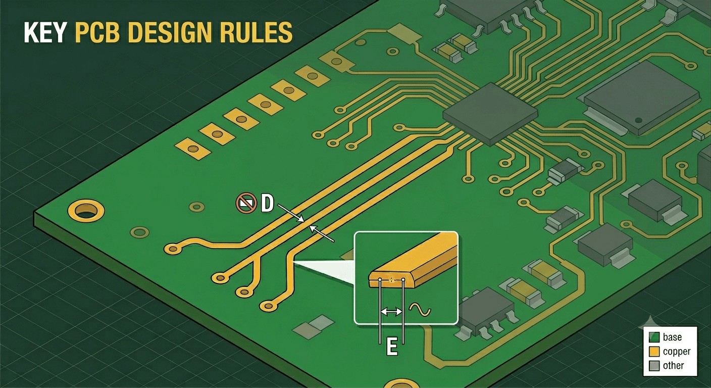
Visual comparison between trace spacing (edge-to-edge distance between copper conductors) and clearance (safety envelope between traces and non-trace features).
Difference Between Trace Spacing and Clearance
-
Definition
The edge-to-edge air or dielectric distance between two separate copper conductors on the same layer of the printed circuit board.
-
Purpose
Prevents crosstalk, parasitic interactions, and copper bridging during chemical etching.
-
Definition
A broader safety envelope defined within PCB layout rules, encompassing the minimum spatial gap between a conductive trace and non-trace features.
-
Purpose
Ensures safe isolation from unplated through-holes (NPTH), mechanical board edges, mounting hardware, and component pads.
The Role of Trace Width and Spacing in PCB Design
Selecting the correct pcb trace width and spacing is a delicate balancing act between thermal capacity, impedance targets, and routing real estate. Trace width is predominantly governed by the target net's current-carrying requirements and maximum allowable temperature rise, as calculated via IPC-2152 standards.
Conversely, the spacing between those traces governs the voltage isolation and electromagnetic coupling. When you narrow the trace width to fit dense BGA fan-outs, you must dynamically scale the adjacent pcb trace spacing to maintain uniform characteristic impedance. Disruptions in this spatial ratio introduce localized impedance discontinuities, triggering signal reflections that degrade high-speed digital wavefronts.
Key Factors Influencing PCB Trace Spacing Rules
Setting up an effective matrix of pcb clearance rules requires a deep understanding of the physical phenomena that occur when current flows through copper embedded in an epoxy-glass matrix.
Dielectric breakdown occurs when the electric field between adjacent traces exceeds the substrate material's dielectric strength, causing permanent short circuits.
Voltage Levels and Dielectric Breakdown
The primary structural reason for enforcing strict pcb trace spacing is to counteract dielectric breakdown. When a significant potential difference (voltage) exists between two adjacent traces, an electric field is generated across the insulating gap. If the field intensity exceeds the dielectric strength of the substrate material (such as standard FR-4, which typically exhibits a dielectric strength of approximately 20 kV/mm to 30 kV/mm), the material can break down.
This results in carbon tracking or direct electrical arcing, leading to permanent short circuits and physical board destruction.
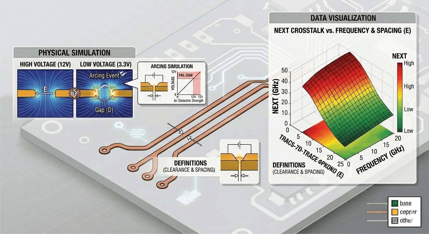
Crosstalk and Parasitic Capacitance in High-Speed Signaling
In high-speed digital architectures, parallel traces behave like unintended distributed capacitors and transformers. Crosstalk occurs when the electromagnetic field generated by an aggressive (switching) net couples energy onto an adjacent victim net.
The 3W Rule
To mitigate crosstalk, high-speed layout methodologies enforce the 3W Rule. This principle states that the distance between trace centerlines must be at least three times the width of a single trace (3W), meaning the clear pcb trace spacing between the inner edges must be equal to or greater than twice the trace width (2W). Adhering to this spatial isolation reduces mutual inductance and parasitic capacitance, effectively eliminating up to 70% of potential crosstalk.
Manufacturing Defect Risks: Copper Slivers and Bridges
From an industrial fabrication standpoint, squeezing pcb trace spacing past conservative thresholds introduces severe yield risks. During the photolithographic printing and subsequent chemical etching phases of PCB manufacturing, liquid etchant is sprayed onto the board to dissolve unprotected copper.
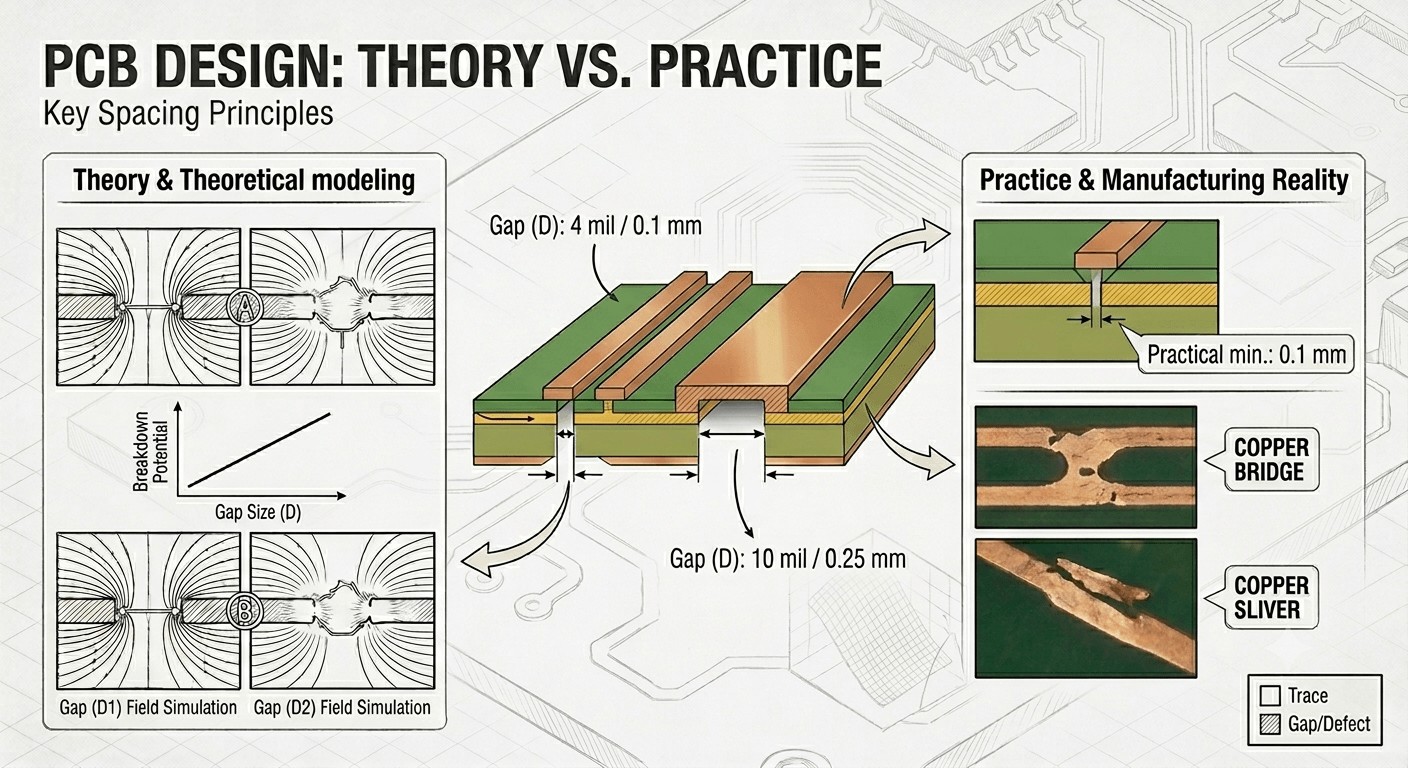
Excessively narrow trace gaps can trap chemical etchant due to surface tension, causing copper bridges (short circuits) or detached copper slivers that shift during assembly.
If the gap between two traces is excessively narrow, the chemical fluid can become trapped due to surface tension, resulting in incomplete etching. This manifests as a copper bridge (a direct short circuit) or an unstable copper sliver (detached, floating micro-fragments of copper that can shift during assembly and short out nearby connections).
Environmental Conditions (Pollution Degree and Moisture)
A circuit board operating inside a sealed, climate-controlled server chassis requires far less spacing than an industrial automotive sensor exposed to atmospheric moisture, salt fog, and conductive dust. Environmental contaminants lower the effective surface resistance of the board substrate. Moisture absorption promotes electrochemical migration (dendritic growth), where microscopic copper tendrils slowly grow across the trace spacing gap under electrical bias, eventually shorting the circuit. High-quality liquid photoimageable (LPI) solder mask acts as a vital physical barrier against these environmental hazards.
Industry Standards for PCB Clearance: IPC-2221 and Beyond
Rather than guessing at spacing values, professional hardware designs rely on the baseline empirical frameworks established by the Association Connecting Electronics Industries (IPC).
Overview of the IPC-2221 Standard Table
The foundational document governing board geometries is IPC-2221B (Generic Standard on Printed Board Design). Section 6.3 provides explicit matrices calculating the minimum electrical clearance based on voltage, atmospheric altitude, and whether the conductors are placed on internal layers, unprotected external layers, or external layers coated with a permanent solder mask.
| Voltage Potential Difference (DC or AC Peak) | Internal Conductors (B1) | External Conductors, Uncoated (B2) | External Conductors, Coated with Solder Mask (B4) |
|---|---|---|---|
| 0 – 15 V | 0.05 mm (2 mil) | 0.10 mm (4 mil) | 0.05 mm (2 mil) |
| 16 – 30 V | 0.05 mm (2 mil) | 0.10 mm (4 mil) | 0.05 mm (2 mil) |
| 31 – 50 V | 0.10 mm (4 mil) | 0.60 mm (24 mil) | 0.13 mm (5 mil) |
| 51 – 100 V | 0.10 mm (4 mil) | 0.60 mm (24 mil) | 0.13 mm (5 mil) |
| 101 – 150 V | 0.20 mm (8 mil) | 0.60 mm (24 mil) | 0.40 mm (16 mil) |
| 151 – 300 V | 0.20 mm (8 mil) | 1.25 mm (50 mil) | 0.40 mm (16 mil) |
| 301 – 500 V | 0.25 mm (10 mil) | 2.50 mm (100 mil) | 0.80 mm (32 mil) |
Important Note
For voltages exceeding 500V, the required pcb trace spacing escalates linearly, requiring explicit calculations or specialized creepage management techniques like routing physical isolation slots through the substrate material.
IPC-9592B for Power Conversion Applications
For engineers designing switch-mode power supplies (SMPS), computer servers, or power conversion equipment, IPC-2221 parameters are often insufficient. Instead, IPC-9592B provides highly stringent requirements tailored specifically for power conversion electronics, defining trace clearance rules based on functional, basic, and reinforced insulation classifications to ensure long-term product lifespans under continuous thermal and electrical stress.
How to Calculate and Optimize PCB Trace Spacing
Optimizing a high-performance design requires moving past arbitrary default values in your EDA software and executing a structured Design for Manufacturability (DFM) approach.
Modern PCB design tools incorporate trace width and spacing calculators that use substrate properties to determine exact physical dimensions for controlled-impedance routing.
Using PCB Trace Width and Spacing Calculators
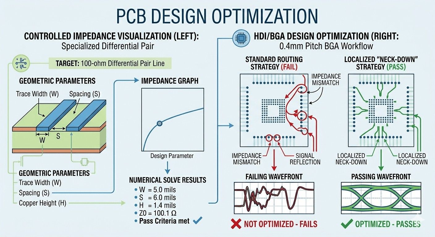
Modern layout pipelines leverage numeric solvers to automate routing geometries. When configuring high-frequency nets, designers utilize specialized trace width and spacing calculators alongside field solvers to target specific characteristic impedances (typically 50-ohm single-ended or 100-ohm differential pairs).
By inputting the substrate's relative permittivity (Er or Dk), the copper weight, and the target dielectric height determined by the layer stackup, you can accurately calculate the exact physical dimensions required for your board.
Best Practices for High-Performance and High-Density PCBs (HDI)
When breaking out high-pin-count components like 0.4 mm pitch BGAs or complex system-on-chips (SoCs), standard routing clearances quickly become unmanageable. In these High-Density Interconnect (HDI) environments, designers must employ localized neck-down strategies:
-
Escape Routing
Drop the trace width and pcb trace spacing within the tight boundary of the BGA matrix down to the manufacturer's absolute limits.
-
Impedance Matching
Once the signal trace clears the dense perimeter of the IC component, widen the trace and expand the adjacent spacing back out to standard dimensions to maintain controlled impedance and minimize signal attenuation.
-
Orthogonal Routing
Ensure that high-speed signal lines running on adjacent layers are routed orthogonally (perpendicularly) to one another, preventing vertical broadside crosstalk.
Navigating Manufacturer Capabilities: Why JLCPCB is Your Best Choice
A theoretically perfect PCB layout is useless if it cannot be reliably produced on a factory floor. To ensure high production yields and minimize unit costs, your design rules must directly align with your fabrication partner's real-world manufacturing limits.
JLCPCB's Precision Limits for Trace Width and Spacing
As a global leader in printed circuit board fabrication, JLCPCB operates advanced, highly automated factories capable of delivering exceptional resolution and structural accuracy. The absolute minimum allowable pcb trace width and spacing are heavily dependent on the chosen layer count and base copper thickness (weight) of the design.
To maintain optimal process control and high production yields, JLCPCB establishes precise operational boundaries:
| PCB Type / Layer Count | Base Copper Weight | Minimum Trace Width | Minimum Trace Spacing |
|---|---|---|---|
| 1-Layer / 2-Layer FR4 | 1 oz (35 µm) | 0.10 mm (4 mil) | 0.10 mm (4 mil) |
| Multilayer (4 to 20 Layers) | 1 oz (35 µm) | 0.09 mm (3.5 mil) | 0.09 mm (3.5 mil) |
| BGA Fan-out Only (Multilayer) | 1 oz (35 µm) | 0.076 mm (3 mil) | 0.076 mm (3 mil) |
| Double-Sided Board | 2 oz (70 µm) | 0.16 mm (6.5 mil) | 0.16 mm (6.5 mil) |
| Multilayer Board | 2 oz (70 µm) | 0.16 mm (6.5 mil) | 0.20 mm (8 mil) |
| Heavy Copper Board | 3.5 oz (122.5 µm) | 0.25 mm (10 mil) | 0.25 mm (10 mil) |
Design Note
While JLCPCB's precision manufacturing can process 3.5 mil limits on standard multilayer designs, engineering best practices recommend utilizing a standard production baseline of 4 mil or wider wherever space permits. This approach optimizes production yields and ensures the lowest possible fabrication costs.
Advanced Etching and Quality Control Inspection
JLCPCB maintains these tight tolerances through massive capital investments in cutting-edge fabrication equipment. Standard manual wet-etching lines are replaced with automated vacuum etching systems that minimize the lateral "under-cutting" of copper traces. This ensures that the physical cross-sections of finished traces closely match the idealized rectangular profiles defined in your Gerber design files.
Furthermore, 100% of multilayer orders undergo rigorous Automated Optical Inspection (AOI). Highly precise digital camera arrays scan every layer of the processed copper, automatically comparing the physical board against the original CAD data to flag any sub-mil copper bridge or neck-down defect before the layers are laminated together.
Cost-Effectiveness Without Compromising Manufacturing Tolerance
Historically, specifying sub-5-mil traces meant accepting astronomical prototype costs and long lead times. JLCPCB has disrupted this convention by applying intelligent panelization algorithms and high-volume automation.
By running highly standardized, continuous-feed manufacturing lines, they minimize material waste and setup overhead. This allows engineers worldwide to prototype precision, high-density multi-layer boards using advanced trace geometries at an accessible price point, without sacrificing structural quality or mechanical tolerance.
FAQ about PCB Trace Spacing Optimization
Q: What is the difference between PCB trace spacing and clearance?
Trace spacing refers specifically to the edge-to-edge distance between two copper conductors on the same layer, focusing on crosstalk prevention and manufacturing defects. Clearance is a broader safety concept that covers the minimum distance between a trace and non-trace features such as board edges, mounting holes, and unplated through-holes.
Q: What is the 3W rule and why is it important?
The 3W rule states that the center-to-center distance between parallel high-speed traces should be at least three times the trace width (3W), meaning the edge-to-edge spacing should be at least 2W. This spatial isolation reduces mutual inductance and parasitic capacitance, eliminating up to 70% of potential crosstalk in high-speed digital designs.
Q: How do I determine the minimum trace spacing for my voltage level?
Refer to the IPC-2221B standard table (Section 6.3), which provides minimum electrical clearance values based on voltage potential, conductor placement (internal vs. external), and whether a solder mask coating is applied. For power conversion applications, use the more stringent IPC-9592B standard.
Q: What are the minimum trace width and spacing capabilities at JLCPCB?
JLCPCB supports minimum trace width and spacing of 3.5 mil (0.09 mm) for standard multilayer designs with 1 oz copper, and 3 mil for BGA fan-out areas. For 2 oz copper, minimums increase to 6.5 mil for width and 8 mil for spacing on multilayer boards.
Q: What happens if trace spacing is too narrow during manufacturing?
Excessively narrow trace spacing can cause copper bridges (unintended short circuits) or copper slivers (floating copper fragments) during chemical etching. Etchant can become trapped due to surface tension in tight gaps, leading to incomplete etching and significant yield losses.
Conclusion on PCB Trace Spacing Optimization
Optimizing your board's trace spacing requires balancing electrical physics with structural manufacturing limits. By pairing conservative layout strategies with the advanced production capabilities of an industry leader like JLCPCB, you can easily deliver high-reliability, high-performance designs.
Final Layout Checklist Before Fabrication
Before exporting your production Gerber, ODB++, or IPC-2581 files and uploading them to the JLCPCB online quote system, run through this comprehensive DFM pre-flight check:
- Verify Base Copper Alignment: Check that your minimum trace width and spacing rules match the specific requirements of your chosen copper weight (e.g., maintaining at least 6.5 mil spacing for 2 oz copper layers).
- Execute Design Rule Checks (DRC): Ensure your EDA software's DRC engine is configured to match JLCPCB's manufacturing capabilities, checking for any accidental spacing violations.
- Apply the 3W Rule on High-Speed Nets: Confirm that critical high-frequency signal lines, clock signals, and differential pairs have sufficient spatial isolation from adjacent nets to prevent crosstalk.
- Review High-Voltage Clearances: Cross-reference all high-voltage nodes against IPC-2221B standards to guarantee adequate physical spacing under solder mask coatings.
- Enable Controlled Impedance Mode: If your design features matched-impedance transmission lines, select JLCPCB's Controlled Impedance option during ordering to access precise +/-10% layer stackup tolerances.
Popular Articles
• Understanding the Basics of Electronic Devices and Circuits
• Choosing the Right Electronic Components for Your Electronic Design: Tips and Best Practices
• PCBs Explained: A Simple Guide to Printed Circuit Boards
• Guide to the Top 10 Commonly Used Electronic Components
• Digital 101: Fundamental Building Blocks of Digital Logic Design
Keep Learning
Understanding the Basics of Electronic Devices and Circuits
In the realm of modern technology, electronic devices and circuits play a crucial role in powering everything from everyday gadgets to complex machinery. Understanding the fundamentals of these components can provide valuable insights into how various electronic systems operate and interact. This blog explores the basics of electronic devices and circuits, their types, functions, and the significance of their design in today's technological landscape. Electronics means the study of the flow of electro......
Optimize PCB Trace Spacing for High-Performance PCBs
Key Takeaways Trace Spacing vs. Clearance: Trace spacing is the edge-to-edge distance between copper conductors on the same layer, while clearance encompasses the broader safety envelope between traces and non-trace features like board edges and mounting holes. The 3W Rule: For high-speed signals, maintain at least 3x the trace width between centerlines (2W edge-to-edge spacing) to reduce crosstalk by up to 70%. IPC-2221 Standards: Industry-standard clearance values depend on voltage levels, altitude,......
PCB Board Outline: Smart Design Tips for Seamless Manufacturing
Key Takeaways Board Outline Defined: The closed polygonal contour on Mechanical Layer 1 that defines your PCB's final physical boundary, including cutouts, slots, and mounting holes. Why It Matters: Directly impacts enclosure fit, mechanical stability, assembly efficiency, and production yield — a well-designed outline reduces costs and lead times. Critical Parameters: Maintain ≥0.2 mm edge clearance, use ≥0.5–1.0 mm corner radii, and specify tolerances appropriate to your routing method (±0.1 mm prec......
Dimensional Stability in PCB Manufacturing: Precision Solutions for Reliable PCBs
Key Takeaways Dimensional stability is a PCB’s ability to maintain precise dimensions and flatness under thermal, humidity, and mechanical stresses. It is essential for accurate layer registration, preventing warpage, via cracks, and assembly failures in multilayer boards. Achieving this requires high-Tg FR-4 materials with low CTE, symmetric stack-ups, balanced copper, and tightly controlled lamination. Professional manufacturing delivers <0.75% bow/twist and ±0.1 mm tolerances, ensuring higher yield......
Types of PCB Boards: Ultimate Reference with Specs & Use Cases
A printed circuit board (PCB) consists of laminated insulating and conductive materials that connect multiple electrical devices. A PCB can be thought of as a layered composite of fibreglass and epoxy with copper patterns etched onto it. These serve as electrical conductors and pathways for signals and power. A PCB can be Simple (one layer of conductive material), Double-Sided (two conductive layers), or Complex (three or more conductive layers) to allow numerous circuit paths on a small piece of hard......
PCB Layers Explained : Building Better Boards Through Smart Stackup, Standards, and Design Practices
A PCB is a sandwich of copper and insulating sheets that are stacked together to form a circuit board. Each PCB layer has a specific purpose; for example, some carry signals (traces connecting components), while others serve as solid planes for power or ground. Think of PCB layers like the floors in a building, where each floor can have a different role. We can think of it as offices (signals) on one floor and storage (ground/power) on another. The number of layers varies by design complexity, from ju......