Via Stitching Guide : Core Functions, Pitch Rules & Placement
17 min
- What Is Via Stitching and How Does It Work?
- Core Functions of Via Stitching in PCB Layout
- Best Practices for Via Stitching Placement
- Manufacturing High-Density Via Stitching Boards
- FAQs About Via Stitching
- Conclusion
key takeaway
- Core Purpose: Ties ground layers together to cut EMI, reduce impedance, and shorten return paths.
- Pitch Rules: Space vias at λ/10 for ground grids and λ/20 for edge rings and shielding fences.
- Layer Transitions: Place stitching vias adjacent to signal vias to minimize return current loop area.
- Avoid Over-Stitching: Overuse perforates power planes, alters trace impedance, and increases drilling costs.
- DFM Control: Follow hole spacing rules, tent non-test vias, and maintain proper edge copper setbacks.
Via stitching connects ground copper across different PCB layers using rows or grids of vias, helping the layers form a continuous, low-impedance ground reference. These stitching vias create short return current paths, enhance grounding, and help reduce electromagnetic interference (EMI). The distance between vias, or via pitch, depends on the highest significant signal frequency, the signal's wavelength in the PCB material, and the board layout.
In this guide, we will discuss how stitching vias work, how they carry return current, and why they're so important in PCB layout. Also included are instructions on calculating pitch using the signal wavelength, where to place stitching vias along the board edges, and how to avoid excessive stitching.
What Is Via Stitching and How Does It Work?
Via stitching is the act of inserting a "via" between two copper areas on different layers; these vias are typically plated, tied to the same net, and grounded. The vias cause those areas to behave as a single conductor, keeping the return current and fields where the layout wants them.
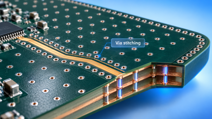
Figure 1: Via stitching on a four-layer PCB with a ground via grid, a via fence along
Understanding Via Stitching in High-Frequency Design
A stitching via is a via that is not included in the signal. It brings together the ground copper of each layer it crosses: outer-layer pours, inner ground planes, and a ground area that might not be connected. Because the copper resistance is low, a single via at DC connects two ground layers that are at nearly the same potential. Each via also introduces a small series inductance to the connection, in the high-frequency case.
Howard Johnson's approximation for a via of height h and drill diameter d, both in inches, is L ≈ 5.08h[ln(4h/d) + 1] nH.
Example: A 0.3 mm (12 mil) via through a 1.6 mm (63 mil) board results in about 1.3 nH.
This is approximately 8 Ω of reactance at 1 GHz. So at high frequency, one via can't maintain two planes at the same potential, and via stitching solves this problem in two ways:
- Parallel vias: Many vias in parallel reduce the net inductance between layers.
- Short spacing: Closely spaced vias keep the gaps between them small enough to limit field leakage and to raise the plane-pair resonance.
Via Stitching for Ground Plane Continuity and Return Current Paths
When the frequency is high, the return current will flow in the reference plane immediately under the signal line. This path has the smallest loop area and hence the lowest inductance. When moving a trace from one layer to another, the reference plane often changes. The return current then has to travel between the two planes at the transition, and the layout determines the path:
- Ground-to-ground transition: A via stitch that connects the signal via to the return path that provides a short path with minimal inductance between the planes.
- Ground-to-power transition: A via cannot connect planes on different nets; instead, a decoupling capacitor is placed near the transition where the return current flows.
- No nearby return path: Return current is diffused through the plane-pair cavity and finds a path that widens the loop and introduces noise into other vias.
For a single-ended signal via, the distance to the nearest stitching vias is a major factor in the via's impedance. Return vias are not an independent grounding detail, but are part of the transmission line.
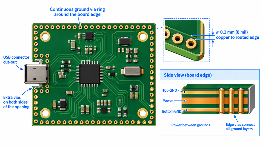
Figure 2: Return current crossing between two ground planes through a stitching via
Stitching vs. Thermal vs. Shielding Vias
These are all plated holes, which may be the same size drill. The shielding vias are stitching vias used in series to contain fields; they are not necessarily different from stitching vias, but vary in placement and pitch. Thermal vias serve different purposes and therefore have different locations and pitches.
| Via Type | Primary Function | Typical Location | What Sets the Pitch |
|---|---|---|---|
| Stitching via | Tie the ground copper on several layers into one low-impedance reference | Across ground pours and planes, and next to signal vias that change layers | Wavelength at the highest frequency of concern |
| Thermal via | Conducts heat from a component's thermal pad into the inner or bottom copper | Arrays under exposed pads of QFNs, regulators, LEDs, and power MOSFETs | Pad size, heat load, and solder-wicking limits |
| Shielding via (via fence) | Confines fields around a trace or circuit to reduce coupling and emission | Rows along RF or high-speed traces and around sensitive circuits | Wavelength, typically λ/20 or tighter |
Core Functions of Via Stitching in PCB Layout
In PCB layout, there are three primary functions of via stitching. It manages EMI, minimizes the impedance between ground layers, prevents plane-cavity resonance, dissipates heat, and ensures power integrity. The electrical functions are the primary ones, with heat spreading as a secondary effect.
Minimizing EMI with Via Stitching and Via Fences
A via fence is a line of vias that are connected to ground along a trace or around a circuit. Every segment between two vias acts as an aperture in a shield and radiates efficiently when it is nearly half a wavelength long.
Gary Fenical's aperture rule of thumb is that the shielding effectiveness of a single slot of length L is approximately SE = 20·log10(λ/2L) dB. It was applied to a gap in a fence and provided these estimates:
- Gap of λ/10: about 14 dB for a single gap.
- Gap of λ/20: about 20 dB for a single gap.
- Several gaps: the estimate decreases by 20·log10(n) when n gaps lie within half a wavelength, so a long fence shields less than one gap would suggest.
According to the same source, apertures should be chosen to be smaller than λ/50, but no larger than λ/20. These figures are for comparison of pitches only and do not indicate a result in an emissions test.
There are 3 common locations for the use of fences:
- RF and high-speed traces: Coupling into adjacent traces is minimized by a fence tied to the plane below, on each side of the trace.
- Grounded coplanar waveguide: The fence is used to lower the coplanar ground to the plane potential to ensure that the unwanted parallel plate modes between the two ground layers are suppressed.
- Noisy circuits: A ring around a switching regulator or clock generator limits field coupling into analog circuits.
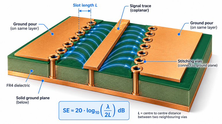
Figure 3: Via fence on both sides of a high-speed microstrip trace, with the fence pitch marked as a fraction of wavelength.
Reducing Ground Impedance Between Inner Layers
Stitching reduces the impedance between ground layers by using multiple parallel vias in series. A 1 GHz connection with the 8 Ω connection is made through ten 1.3 nH vias that are a large distance apart so that the mutual inductance is small.
A cavity is created by two parallel ground planes or a plane and a large pour. The cavity is allowed to couple noise between the vias that pass through it at resonance. The cavity is broken up into smaller cells by a stitching grid, which increases the lowest resonance.
There are three layout settings to accommodate this:
- Direct connection: Make stitching vias directly connected to planes and pours, since the thermal-relief spokes introduce inductance.
- All ground layers: Stitch each stitching to all ground layers that it passes through.
- No floating copper: Stitch or remove isolated areas of ground, as floating copper can lead to noise coupling between nearby traces.
Best Practices for Via Stitching Placement
The stitching placement begins with the highest frequency the board must have. Take that frequency and calculate the wavelength in the dielectric, and use a fraction of that as the maximum pitch. Edge rules and over-stitching then refine the grid.
Via Stitching Pitch and Spacing Rules for High-Speed Signals
There is no one-size-fits-all solution when it comes to pitch. The distance between maximum points is suggested to be < λ/8 and < λ/20 of the wavelength at the highest frequency of interest:
- λ/8: Writing in EDN, Steve Hageman says that if the ground vias are spaced 1/8 λ or less, the ground plane acts as a solid ground.
- λ/10: A common general-purpose limit for ground stitching in fabricator and design guides.
- λ/20: The common rule of thumb for via fences and shielding, consistent with Fenical's limit for apertures.
The pitch for a specific board follows four steps:
- Find the highest frequency of concern. For digital signals, estimate bandwidth from the 10–90% rise time with f ≈ 0.35 / tr; a 100 ps edge gives 3.5 GHz.
- Calculate the wavelength in the dielectric. Use λ = c / (f × √Dk). For stripline, use the laminate Dk.
- Choose the fraction. Use λ/10 for general ground stitching, and λ/20 for via fences and board edges.
- Check the result against the fabricator's limits. Confirm the minimum via size and hole-to-hole spacing before committing to a dense grid.
| Highest Frequency | Wavelength in FR4, Dk 4.2 (mm) | λ/10 Pitch (mm) | λ/20 Pitch (mm) |
|---|---|---|---|
| 1 GHz | 146 | 14.6 | 7.3 |
| 2.4 GHz | 61 | 6.1 | 3.0 |
| 5 GHz | 29.3 | 2.9 | 1.5 |
| 10 GHz | 14.6 | 1.5 | 0.73 |
The effective Dk for microstrip is less than that of the laminate and is typically 3.2-3.3 for a 50 Ω line on FR4 laminate. A shorter wavelength, and hence a conservative pitch, is obtained with the laminate Dk.
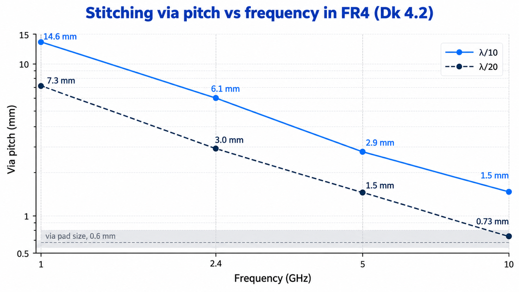
Figure 4: Via stitching pitch versus frequency on FR4, comparing λ/10 and λ/20 spacing
Edge Via Stitching Rules for Board-Level EMI Control
Edge is a stitching method that lays a row of ground vias along the board edge, thereby joining all ground layers at that edge. It helps to reduce fields radiating between pairs of planes along the board edge, which are a major source of radiation at high frequencies.
The rules of the edge ring are 5-fold:
- Pitch: λ/20 at the highest frequency of concern (same as via fence).
- Layers: Connect the ring to all ground layers, and connect a ground pour strip around the outside of the top layers, to allow vias to connect to copper.
- Setback: Copper distance from the routed edge is at least 0.2 mm (8 mil), and the V-cut edge is 0.4 mm (16 mil), according to JLCPCB's capabilities.
- Continuity: Stitch in the same direction around ring openings and cut-outs, and don't break the stitching inside the ring.
- Power planes: If possible, place power planes between ground planes, as stitching cannot connect a power plane to a ground plane. A power plane sandwiched between two edge-stitched ground planes has less radiation leakage from the edges.
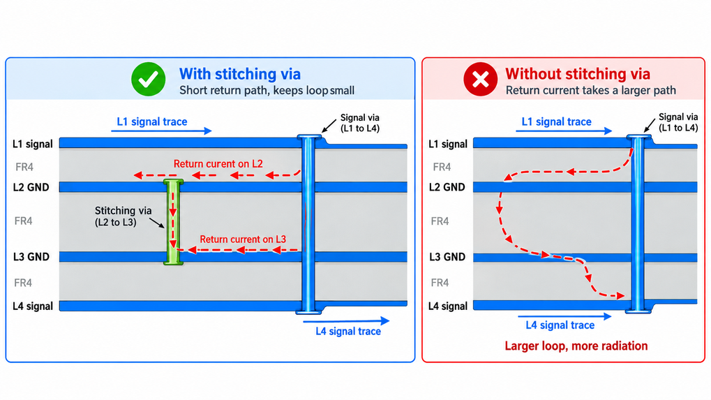
Figure 5: Edge via stitching ring along a PCB perimeter, with the copper setback from the routed edge marked.
Avoiding Signal Degradation from Over-Stitching
Over-stitching provides more vias than needed by return paths and fields. This reduces the power planes, alters the impedance of adjacent traces, and introduces drill count, so stitching vias should be stitched in where a return path or a fence is required.
| Over-Stitching Effect | Mechanism | Layout Fix |
|---|---|---|
| Perforated power planes | Each through via crossing a power plane needs an antipad, a clearance opening in the plane copper, and dense rows of antipads merge into a slot | Use the pitch the frequency requires, and no tighter, and stagger rows |
| Shifted trace impedance | Ground pour, and vias close to a trace add capacitance, which turns a microstrip into a grounded coplanar waveguide | Include the pour and fence in the field-solver model, or widen the gap |
| Routing blockage | Via grids occupy inner-layer routing channels | Keep channels clear under dense routing areas |
| Drill count and cost | More holes and smaller drill lengths lengthen drilling time | Use the pitch the frequency requires, with 0.3 mm or larger holes, where the pitch allows |
JLCPCB (0.2 mm inner-layer via-to-copper clearance) will clear a 0.7 mm (28 mil) circle in a power plane with a 0.3 mm (12 mil) via. The copper webs between antipads are 0.3 mm (12 mil) wide, at 1 mm (39 mil) pitch.
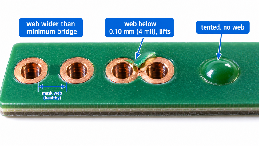
Figure 6: Comparison showing antipads in a power plane at 1 mm pitch and merging into a slot at 0.75 mm pitch.
Manufacturing High-Density Via Stitching Boards
These dense via-stitching arrays create three design-for-manufacturability (DFM) concerns: drill-position error when drilling small holes, thin or cracked barrel plating when drilling deep holes, and narrower solder-mask dams than the fabricator's minimum. Each design decision is performed before release.
Drilling Accuracy and Layer Registration for Dense Via Arrays
Position errors in the holes during drilling and layer-to-layer registration errors both cause the holes to be displaced relative to the pads. The annular ring in each layer must absorb that energy transfer; otherwise, the drill can break out of the pad.
JLCPCB's PCB capabilities page lists these drilling capabilities for vias:
- Minimum via: 0.15 mm hole with a 0.25 mm pad; 0.1 mm or 0.2 mm is available only for boards 1 mm thick or less with an ENIG or OSP finish.
- Surcharge: 0.1 or 0.15 mm holes at any pad size, and 0.2 or 0.25 mm holes with pads under 0.45 mm cost more.
- Hole position tolerance: ±0.075 mm.
- Via hole-to-hole spacing: 0.2 mm.
- Via hole to track: 0.2 mm.
A 0.25/0.15 mm via does not leave much room for drill-position errors, as it allows only a 0.05 mm annular ring. A 0.3 mm (12 mil) hole in a 0.6 mm (24 mil) pad leaves a 0.15 mm ring and avoids both surcharges.
Hole Wall Plating Thickness and Barrel Reliability
The thickness of the barrel plating will influence whether the stitching via cracks during repeated thermal cycling. All of the expansion in the barrel is due to the laminate's expansion through its thickness compared to copper, and it occurs with every reflow and temperature cycle.
A common lead-free FR4 material, Isola 370HR, has a Z-axis expansion rate of 45 ppm/°C below its Tg and 230 ppm/°C above its Tg. Copper has an expansion rate of approximately 17 ppm/°C, causing the barrel to stretch and potentially crack thin plating, usually in the middle of the hole.
Three design features protect the barrel:
- State the class: IPC-6012F defines the minimum copper thickness for each performance class, and Class 3 has a thicker copper wall than Class 2. Indicate the class on the fabrication drawing.
- Understand the default value: JLCPCB provides an average hole plating thickness of 18µm.
- High aspect ratio: Plating solution does not flow as easily into high-aspect-ratio holes. A 0.3 mm hole in a 1.6 mm board is about 5:1, while a 0.15 mm hole is nearly 11:1.
DFM Checks for Solder Mask Dams and Via Tenting'
When a stitch array is dense and near a pad, the solder mask will form narrow dams between openings. If it's smaller than the fabricator's minimum solder mask bridge, a dam is not reliable, and solder can flow from a pad to an exposed via.
| DFM Check | JLCPCB Capability | Relevance to Via Stitching |
|---|---|---|
| Minimum pad spacing that keeps a mask dam, 1 oz copper | 0.10 mm (green, red, yellow, blue, purple); 0.13 mm (black, white) | A narrower gap between a pad and an exposed via loses its dam |
| Minimum pad spacing that keeps a mask dam, 2 oz copper | 0.20 mm (any color) | Thicker copper needs a wider gap |
| Via plugging with solder mask | Via 0.5 mm or smaller, no mask opening on either side, at least 0.35 mm from other openings | Plugged stitching vias near pads must respect the opening clearance |
| Copper to routed or V-cut edge | At least 0.2 mm or 0.4 mm | Edge stitching rings must respect the setback |
| Inner-layer via hole to copper | 0.2 mm | Sets the antipad size and the web width between vias |
Four checks complete the DFM review:
- Tent stitching vias: Cover vias that are not test points with solder mask (via tenting) to remove the mask openings that create narrow dams.
- Keep exposed vias out of pads: Place vias in pads only with a via-in-pad process that fills and caps them.
- Run DRC with fabricator rules: Check hole-to-hole spacing, via-to-track clearance, mask dam width, and edge setback before export.
- Verify the Gerber output: The Gerber solder mask layer, not the EDA setting, defines which vias are tented.
FAQs About Via Stitching
Q: How Many Stitching Vias Does a PCB Need?
No fixed count applies because the count follows from the pitch and the area. A 100 mm square pour stitched on a 7.3 mm grid, λ/20 at 1 GHz in FR4, needs about 200 vias.
Q: Should Stitching Vias Be Tented?
In most designs, yes. Tenting removes the mask openings that create narrow dams between stitching vias and nearby pads. Leave a via exposed only when it serves as a test point.
Q: Do Stitching Vias Need Thermal Relief Connections?
No. Stitching vias need a direct, solid connection to planes and pours, because thermal-relief spokes add inductance. Thermal reliefs belong on component pads, where they limit heat sinking during soldering.
Q: Can Blind or Buried Vias Be Used for Via Stitching?
Yes. Blind and buried vias stitch only the layers they span, which keeps routing channels free on other layers. They add fabrication cost, so through-vias remain the usual choice when every ground layer must be bonded.
Conclusion
Stitching is effective when its pitch matches the wavelength at the board's highest frequency and when the vias are located where return current and fields are required. Measure the pitch within the dielectric, then use λ/10 for general stitching, and λ/20 for via fences and board edges, and add a return via at any place where the signal changes ground reference.
This stitching array reduces the ground impedance and edge radiation without destroying power planes or routing channels. After your fabricator approves the array for drilling, plating, and solder mask, upload your Gerber files to receive an instant quote.
Popular Articles
• PCB Silkscreen: All You Need to Know
• The Comprehensive Guide to Circuit Symbols: Key to Understanding Electrical and Electronic Diagrams
• Design Guidelines for PCB Using FR4 Substrates
• Choosing the Best PCB Color-Enhancing Aesthetics and Functionality
• PCB Board Design: A Step-by-Step Guide for Beginners
Keep Learning
Via Stitching Guide : Core Functions, Pitch Rules & Placement
key takeaway Core Purpose: Ties ground layers together to cut EMI, reduce impedance, and shorten return paths. Pitch Rules: Space vias at λ/10 for ground grids and λ/20 for edge rings and shielding fences. Layer Transitions: Place stitching vias adjacent to signal vias to minimize return current loop area. Avoid Over-Stitching: Overuse perforates power planes, alters trace impedance, and increases drilling costs. DFM Control: Follow hole spacing rules, tent non-test vias, and maintain proper edge copp......
Relay Pinout Explained: Diagrams, Pin Functions & Multimeter Testing
Key Takeaways Pin functions: A standard electromechanical relay has two coil pins, and each pole adds a common (COM), normally open (NO), and normally closed (NC) pin. Viewing side: Relay footprints are often drawn in bottom view, with the pins facing you. When a drawing does not state its view, confirm NC and NO with a continuity check. Relay Pin Count: A 5-pin relay is typically SPDT, a 4-pin relay is usually SPST, and an 8-pin relay is commonly DPDT. However, pin arrangements can vary between PCB, ......
How to Connect and Choose a Flyback Diode for a Relay
Key Takeaways Diode Placement: Connect the flyback diode across the relay coil, with its cathode connected to the positive side and its anode to the negative side. Why It Matters: When the relay switches off, the diode provides a safe path for the remaining coil current, preventing a high-voltage spike that could damage the transistor. Choosing the Right Diode: Select a diode with a reverse-voltage rating above the coil supply voltage and a forward-current rating suitable for the coil current. Common ......
A Beginner's Guide to Basic Electronic Components: Functions, Symbols & Uses
Every circuit, from a simple LED flashlight to a microcontroller board, is built from the same handful of common electronic components. This guide breaks down the ten basic electronic components you will encounter most often: What each component does How it works Key specifications Where engineers use it By the end, you will be able to recognize these electronic circuit components on a schematic, a PCB, or a parts bin, and know exactly why each one is there. These electronic components are the buildin......
Reliable BMS Boards Start With Quality PCB Manufacturing
Key Takeaways Dual Duty: BMS PCBs handle heavy currents and millivolt sensing simultaneously, requiring strict layout isolation. Power & Heat: Currents over 10A need 2 oz+ copper pours with via stitching to drop resistance and heat. Clean Sensing: Kelvin differential routing and split grounds prevent load noise from corrupting cell voltage readings. Materials & Finish: High-Tg FR-4 and ENIG surface finishes ensure heat tolerance and flat mounting pads. DFM & Testing: Design for heavy-copper etch toler......
What is Solder Mask and How Does it Impact Your PCB Designs?
Solder mask may not be the most exciting topic in PCB manufacturing, but it's definitely one of the most crucial. Without proper solder mask, your Printed Circuit Boards (PCB's) could suffer from shorts, bridges, corrosion, and other costly and time-consuming issues. So, if you want to ensure the quality, reliability, and longevity of your electronic products, you need to know everything about solder mask - from it's purpose and types to it's application and design implementations. In this ultimate gu......