PCB Power Plane Design for Stable Power Delivery
10 min
- The Essential Role of Power Planes in Modern PCB Layouts
- Step-by-Step Guide to Power Plane Design and Division
- Critical Thermal and Current Handling Factors
- Bridging Design and Manufacturing: Ensuring Plane Integrity with JLCPCB
- FAQ about PCB Power Plane Design
- Conclusion on PCB Power Plane Design
Key Takeaways
- Power planes provide low-impedance DC distribution and signal return paths in modern PCBs
- Split plane design requires careful boundary management to prevent EMI and signal distortion
- Decoupling capacitor placement and loop minimization are critical for power integrity
- Copper weight selection and thermal management ensure reliable current handling
- JLCPCB offers advanced manufacturing capabilities for complex power plane designs
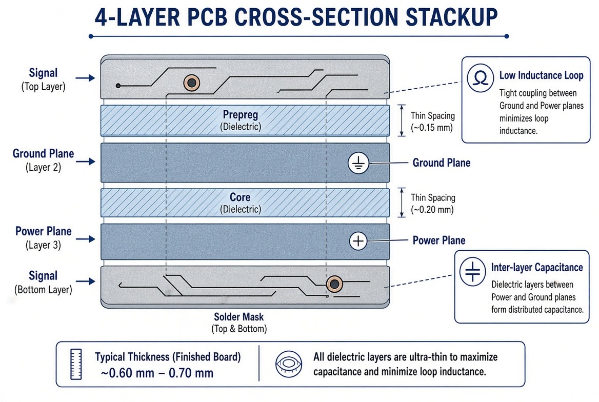
A well-designed power plane serves as the low-impedance backbone of a Printed Circuit Board, distributing continuous direct current (DC) voltage across active components while offering a low-inductance return path for high-speed digital signals. When PCB designers properly plan copper pours, stackup inter-layer capacitance, split planes, and via placement, power distribution networks (PDNs) maintain stable voltage levels even under fast transient load shifts.
The Essential Role of Power Planes in Modern PCB Layouts
Primary Functions: DC Power Distribution and Signal Return Paths
A dedicated power plane replaces narrow copper traces with a continuous copper sheet to distribute DC power efficiently while serving as a high-frequency reference plane for adjacent signal traces. Placing a solid ground plane directly adjacent to a power plane creates a low-inductance loop for signal return currents.
Modern high-speed ICs demand rapid switching current (di/dt) without suffering from transient voltage drop or ground bounce. When a power plane is integrated into a multilayer stackup (such as a standard 4-layer Signal – Ground – Power – Signal or 6-layer Signal – Ground – Signal – Signal – Power – Ground configuration), the continuous copper plane acts as a low-resistance rail across the board.
Beyond delivering VCC to component pins, power planes participate directly in signal integrity. High-frequency signal return currents flow along the path of least inductance, which naturally mirrors the trace directly above or below on the nearest continuous reference copper layer.
How Solid Planes Minimize Impedance and Voltage Drops
Solid planes minimize loop inductance and I^R drop by replacing narrow, inductive trace geometries with wide, low-resistance planar conductors. This low impedance prevents voltage fluctuations across component power pins during transient current spikes.
The effective loop inductance of a power delivery structure depends heavily on the surface area and physical spacing between the power and ground layers. Solid planes eliminate the narrow bottlenecks associated with routing traces, lowering total DC resistance (R) and loop inductance (L).
By keeping plane inductance minimal, high-frequency noise induced by switching ICs remains suppressed across a broad frequency spectrum.
| Design Parameter | Narrow Trace Power Routing | Continuous Solid Power Plane |
|---|---|---|
| DC Resistance | High (10 - 100 mΩ) | Ultra-Low (<1 mΩ) |
| Loop Inductance (L) | High (10 - 50 nH) | Extremely Low (<0.5 nH) |
| Parasitic Capacitance (Cplane) | Minimal (<1 pF) | High (50 - 500 pF/in^2) |
| Thermal Dissipation | Concentrated / Localized | Distributed uniformly across plane |
| EMI Shielding Capability | Poor | Superior (Shields inner signal layers) |
Step-by-Step Guide to Power Plane Design and Division
Solid Planes vs. Split Power Planes: When and How to Split
Split power planes allow designers to supply multiple voltage rails (3.3V, 1.8V, 1.2V) on a single layer, but require careful layout to avoid disrupting signal reference paths. Splitting a plane is appropriate when routing space is limited, provided no high-speed signal traces cross over the split boundaries.
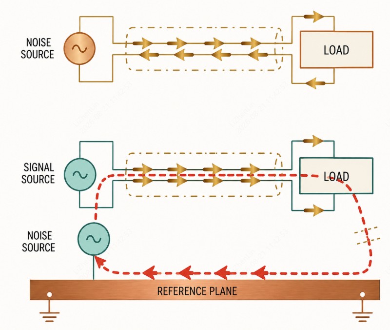
When designing a board with multiple operating voltages, pouring distinct voltage islands on a single inner layer reduces total layer count and overall fabrication cost. However, splitting a plane introduces physical gaps in the copper.
If a high-speed signal trace routes directly over a gap between two distinct power regions, its return current cannot follow the trace smoothly. Instead, the return current must detour around the split gap, creating a loop area that radiates electromagnetic interference (EMI) and causes signal distortion.
Preventing Crosstalk Across Power Plane Boundaries
To eliminate crosstalk and noise coupling across power boundaries, maintain adequate clearance between voltage islands and ensure sensitive traces reference a continuous ground plane. Stitching capacitors or continuous ground reference layers keep noise contained within individual voltage domains.
When splitting a power plane, follow these core guidelines:
Clearance Rules: Maintain a minimum separation of 10 mil to 20 mil 0.25 mm to 0.50 mm) between adjacent power regions to prevent voltage arcing and capacitive crosstalk.
20-H Rule: Keep power plane edges pulled back from the outer ground plane edges by a distance equal to 20 times the inter-layer dielectric thickness (20H). This technique contains fringing magnetic fields within the board boundaries, suppressing radiated EMI.
Avoid Trace Crossings: Never route high-speed digital traces across a split in its reference plane. If crossing a gap is unavoidable, place a decoupling or stitching capacitor (e.g., 10 nF) directly across the split adjacent to the signal trace to provide a bridge for high-frequency return current.
Decoupling Capacitor Placement and Decoupling Loop Minimization
Decoupling capacitors supply local charge during rapid switching events and must be placed as close as possible to IC power pins to minimize parasitic trace inductance. Short, wide vias routed directly down to the power and ground planes maximize capacitor effectiveness.
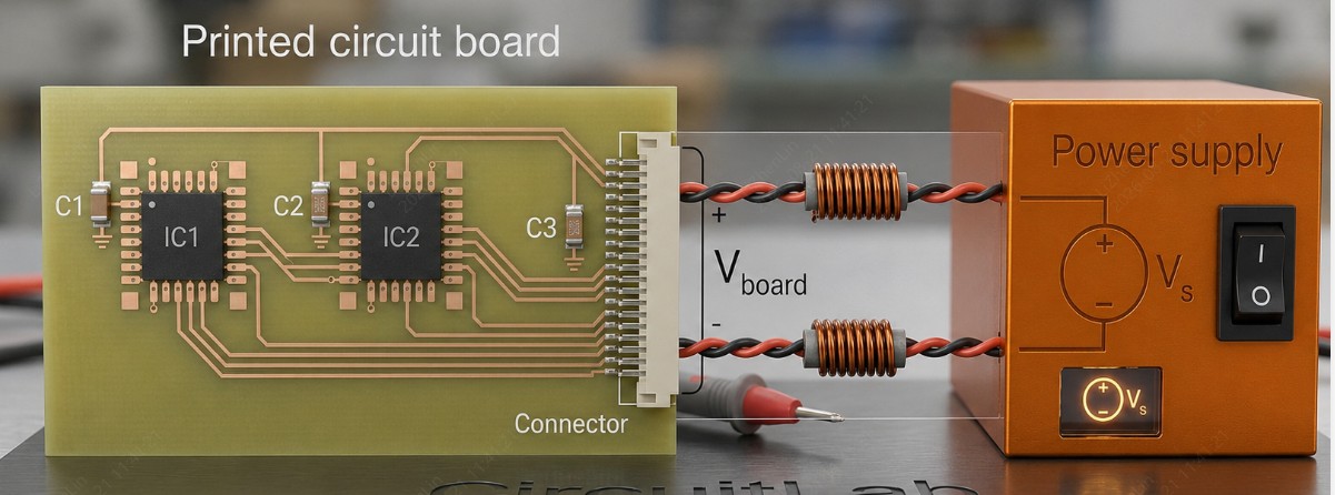
Placing a decoupling capacitor far from an IC pin introduces trace inductance that impedes rapid energy delivery. To optimize plane-level decoupling:
Critical Thermal and Current Handling Factors
Calculating Copper Thickness for High-Current Power Rails
Determining the correct copper weight for a power plane depends on the maximum continuous current, allowable conductor temperature rise, and board layer location. Selecting 1 oz/ft2 (35μm) or 2 oz/ft2 (70μm) copper limits temperature spikes and reduces DC voltage drop across high-power tracks.
IPC-2152 standards define thermal rise relative to trace width, cross-sectional area, and current capacity. While outer layers dissipate heat effectively into ambient air, inner power planes dissipate heat through adjacent dielectric materials, making thermal management a critical consideration.
| Copper Weight | Nominal Thickness (μm) | Recommended Max Current (100 mil Width, 10°C Rise) | Typical Application |
|---|---|---|---|
| 0.5 oz / ft² | 15 - 18 μm | ≈2.5 A | Low-power digital logic, internal signal planes |
| 1.0 oz / ft² | 35 μm | ≈4.5 A | Standard multilayer power planes, general electronics |
| 2.0 oz / ft² | 70 μm | ≈7.5 A | High-current power rails, motor drivers, industrial DC-DC |
| 3.0 oz / ft² | 105 μm | ≈11.0 A | Heavy copper power distribution, automotive equipment |
Thermal Relief Vias and Void Management Near Power Layers
Large copper power planes sink heat away from component pins during soldering, which can lead to cold solder joints if pads are connected directly without thermal relief structures. Using thermal relief spokes balances thermal isolation during assembly with electrical current capacity during operation.
When high-density via arrays pass through an inner power plane, the antipads (clearance holes surrounding drilled vias) can merge into a continuous slot. This void reduces the effective cross-sectional copper area, increasing local current density and localized heating.
Engineers must ensure via pitch leaves sufficient copper neck width between antipads to preserve both current carrying capacity and plane continuity.
Bridging Design and Manufacturing: Ensuring Plane Integrity with JLCPCB
Advanced Multilayer Layer Stackup Control for Low Ground/Power Impedance
Translating power plane designs into reliable physical circuit boards requires tight manufacturing tolerances and consistent dielectric spacing. Industrial fabricators provide pre-validated multilayer stackup options optimized for power plane performance.
For instance, JLCPCB supports multilayer configurations ranging from 2 up to 32 layers. By utilizing thin prepreg layers (such as 7628, 2116, or 1080) and precision core materials, power planes can be located in close proximity to ground reference layers.
Placing a power plane close to a ground plane—with dielectric thicknesses as thin as 0.1 mm—increases inter-layer capacitance, suppressing high-frequency switching noise before it affects sensitive board circuits.
Precision Heavy Copper Fabrication and DFM Clearance Checks
Executing high-current power plane layouts requires careful attention to trace clearances, antipad clearances, and copper weight tolerances. Advanced manufacturing processes ensure heavy copper layers are fabricated cleanly without shorts or excessive etching.
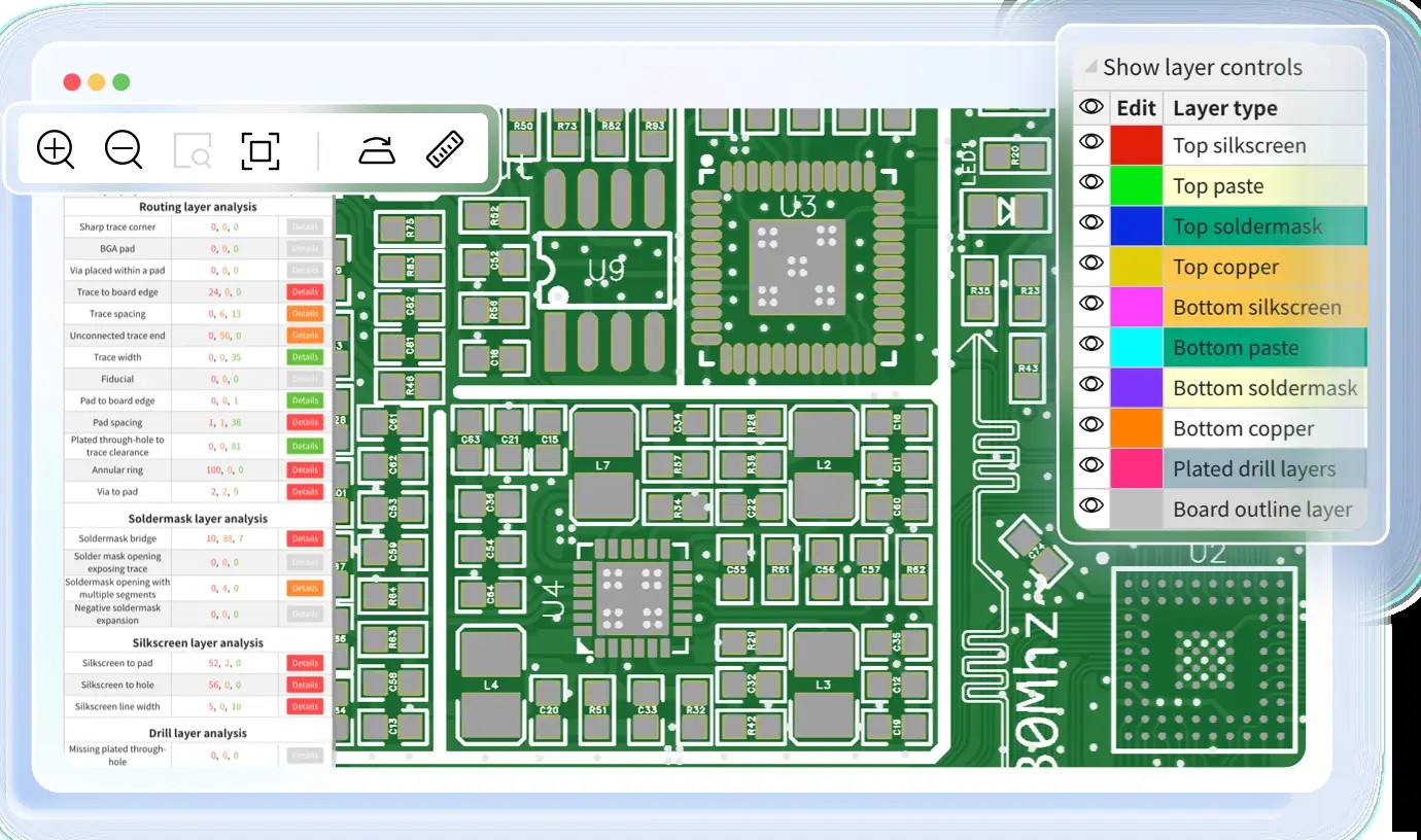
Fabrication specifications provided by JLCPCB support advanced power plane requirements:
FAQ about PCB Power Plane Design
Q: What is the 20-H rule for power planes?
The 20-H rule states that power plane edges should be pulled back from the outer ground plane edges by a distance equal to 20 times the inter-layer dielectric thickness (20H). This technique contains fringing magnetic fields within the board boundaries, suppressing radiated EMI.
Q: How do I choose the right copper weight for power planes?
Select copper weight based on maximum continuous current, allowable temperature rise, and board layer location. For standard applications, 1 oz/ft² (35μm) is common, while high-current applications may require 2 oz/ft² (70μm) or 3 oz/ft² (105μm).
Q: Why are decoupling capacitors important for power planes?
Decoupling capacitors supply local charge during rapid switching events and must be placed as close as possible to IC power pins to minimize parasitic trace inductance. They help maintain stable voltage levels during transient current spikes.
Q: What is the minimum clearance between split power planes?
Maintain a minimum separation of 10 mil to 20 mil (0.25 mm to 0.50 mm) between adjacent power regions to prevent voltage arcing and capacitive crosstalk.
Q: How does JLCPCB support complex power plane designs?
JLCPCB supports multilayer configurations from 2 to 32 layers, offers copper weight up to 3 oz on outer layers, provides minimum trace/clearance down to 3.5 mil, and includes free automated DFM checks for power plane integrity.
Conclusion on PCB Power Plane Design
Designing a high-performance power plane requires balancing critical electrical, thermal, and manufacturing parameters. By optimizing inner-layer stackups, adhering to strict split-plane boundaries, reducing decoupling loop inductances, and sizing copper weights for target thermal loads, engineers can eliminate transient voltage noise and guarantee long-term power delivery stability.
To translate these complex layout strategies into high-yield physical boards, partnering with a precision manufacturer is essential. JLCPCB bridges the gap between advanced CAD design and physical fabrication by providing tight stackup tolerances, heavy copper layer options up to 3 oz, and automated DFM clearance validation. Utilizing pre-validated multilayer stackups through JLCPCB ensures your power plane designs achieve maximum power integrity, low noise, and reliable operation across all product lifecycles.
Popular Articles
Keep Learning
Navigating the Impedance Landscape: Selecting the Right Impedance for USB, Ethernet, HDMI, and SD Card Interfaces
Introduction In the realm of high-speed digital communication, choosing the right impedance is a critical aspect of successful PCB design. Impedance matching ensures optimal signal integrity, minimizes reflections, and enhances the overall performance of interfaces such as USB, Ethernet, HDMI, and SD Card. In this blog post, we'll explore the importance of impedance, the factors influencing impedance selection, and best practices for ensuring reliable data transmission in these widely used interfaces.......
A Beginners Guide to Impedance Control in PCBs
When a digital signal is transmitted from one point to another, it causes a change in the state of the signal line. This change can be understood as an electromagnetic wave moving through the circuit. Reflection occurs when this wave encounters a boundary between different mediums. At this boundary, some of the wave's energy continues as a signal, while the rest is reflected. This process repeats until the energy is either absorbed by the circuit or dissipated into the environment. For electrical engi......
What is PCB Signal Attenuation: How Signals Weaken Over Distance and How to Mitigate It
Key Takeaways Primary Causes: Signal attenuation is mainly caused by skin effect (conductor loss) and substrate energy absorption (dielectric loss). How to Mitigate: Reduce loss by using wider traces, low-loss materials, controlled impedance, and removing via stubs. JLCPCB Solutions: JLCPCB offers Rogers high-frequency laminates, High-TG FR4, precision impedance control, and backdrilling to protect signal integrity. As a signal travels from the source to the load through PCB conductors, the signal is ......
Understanding Analog and Digital Ground in PCB Design
When working on printed circuit board (PCB) design, proper grounding is crucial for ensuring signal integrity, minimizing noise, and maintaining reliable performance. Two common types of ground planes used in PCB layouts are Analog and Digital ground. In this article, we will explore the differences between analog and digital ground, their significance in PCB design, and best practices for their implementation. Analog Ground vs. Digital Ground Analog ground and digital ground have separate purposes in......
Design Guide for USB-3.0 Differential Signaling
In the world of data transfer, USB 3.0 is the Usain Bolt to USB 2.0’s friendly jogger. USB 2.0 is called “High Speed” and limped along at 480 Mb/s, whereas USB 3.0 SuperSpeed rockets up to 5 Gb/s (over ten times faster). But this speed jump brings full‑duplex operation and new differential transmit (SSTX) and receive (SSRX) pairs on dedicated pins. USB 2.0 D+/D– lines handle enumeration and legacy data, while two new 5 Gb/s high‑speed differential pairs carry SuperSpeed data in each direction. While m......
Understanding Impedance Matching for High-Speed PCB Designs
With the advancement of technology and the ever wider application of integrated circuits, the frequency and speed of electronic signal transmission have been increasing, making it essential for PCB conductors to provide high-performance transmission lines. These transmission lines are responsible for delivering signals from a source to the input of a receiver accurately and completely. This requirement emphasizes the need for impedance matching. Electrical impedance, commonly represented as Z and meas......