
EMI Shielding for PCBs : Advanced Techniques and Materials for Superior Electromagnetic Compatibility in Professional Fabrication
11 min
- How EMI Shielding Works on PCBs
- Key EMI Shielding Materials and Their Applications
- Implementing Effective EMI Shielding in PCB Design
- Professional Manufacturing Techniques for Robust EMI Shielding
- Frequently Asked Questions (FAQ)
In essence, EMI shielding is simply the act of enclosing any conductive or magnetic material to ensure the electrical and magnetic fields do not creep in or out of a particular zone on your PCB. Imagine that you had a Faraday cage around your delicate circuits, except that you have to shield not yourself, but your neighbor, against your noisy switching regulator (and the other way around). Modern electronics have become a massive nightmare due to EMI. With clock speeds in the GHz and switching regulators in the megahertz, and wireless radios appearing everywhere on a PCB, the electromagnetic resonance within and around a PCB is extremely cluttered.
Unless you shield your design with EMI, your device may fail regulatory tests (FCC, CE, CISPR), experience self-interference, or even cause interference with surrounding equipment. The stakes are high. A lack of an EMC test may delay a launch by weeks or months, as you hastily apply shielding and filters as a last-minute palliative to an otherwise beautiful product, which is always more costly and finer than doing it right the first time
Common Sources of Electromagnetic Interference in PCBs
To begin with, it will be important to determine the actual source of EMI in order to tame it. High-speed clock signals and harmonics, the inductors and transformers of switching supplies, dumping out both conducted and radiated noise, data links such as USB 3.0, PCIe, HDMI throwing up broadband hiss, RF transmitters and oscillators intentionally beaming, and any fast edge-rate objects that cause little EM fields to ride along with the neighboring traces and cables are the typical suspects on a PCB.
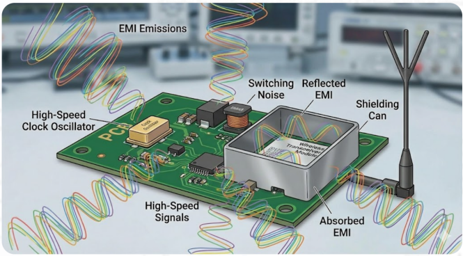
Bad parts may be the only trouble-makers, but even the most ordinary parts may become EMI suspects when the layout is loose. Consider a simple LED driver: when it changes too rapidly, and the current loop area is a mess, it can radiate enough to put you out of a Class B emissions test.
How EMI Shielding Works on PCBs
Principles of Reflection, Absorption, and Grounding
The question is, what is the mechanism of an EMI shield? It is simply dependent on three factors that interact synergistically. At low frequencies, it is primarily reflection. As a wave impinges on a conductive surface, the impedance difference between the free space and the metal causes a large portion of the energy to be reflected. Actually, conductive materials, such as copper or aluminum, are excellent reflectors.
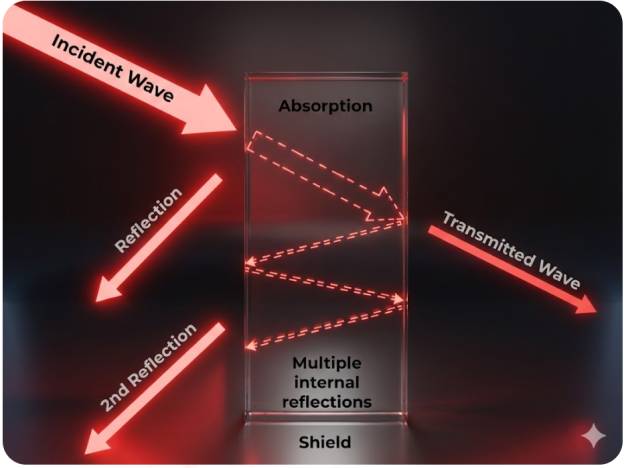
The higher the frequency, the higher the absorption kicks in. The wave enters the shield, and its energy is converted into heat due to resistive losses. Its absorption is determined by the permeability of the material, its conductivity, and its thickness. Inferior shields, shields that are thicker, or have high magnetic permeability- think mu-metal, perform better. Nothing brings it all together like grounding. Unless a shield is well grounded, it will begin to act like an antenna rather than a barrier. Good shielding requires lots of vias to the ground planes, wide stitching patterns, and good solder joints.
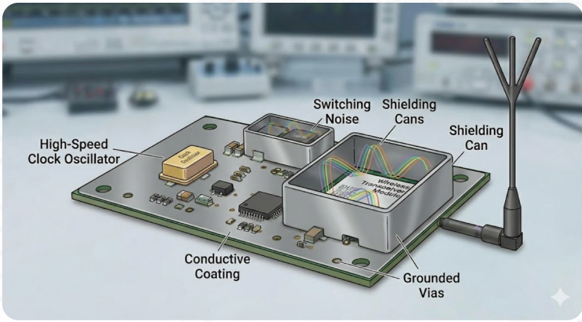
Role of Shielding Layers, Cans, and Conductive Coatings
At the board level, one can shield in a few ways, depending on what you are doing. A solid isolation is provided by shielding cans, metal enclosures soldered onto the PCB over sensitive components, and used in RF modules, wireless equipment, and sensitive analog circuits. They are typically composed of tin-plated steel or nickel silver and are able to block up to 40 -80 dB of EMI depending on construction. Lightweight and flexible conductive coatings and paints are also available in cases where weight or height may be a concern. They are applied with metallic particles (silver, copper, or nickel) incorporated into a polymer and sprayed or painted only on the areas of a car that require it.
On the PCB, special ground copper planes serve the purpose of in-built shield planes. A continuous, uninterrupted ground plane between a noisy layer and a sensitive component reduces coupled noise significantly, which is one of the easiest and least expensive methods of shielding in PCB design.
Key EMI Shielding Materials and Their Applications
Conductive Fabrics, Foils, and Polymer Composites
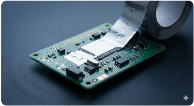
The EMI shielding world is a toolbox to designers, Yo. When you are prototyping or even simply fixing something, copper foil tape remains a mainstay, as it is extremely conductive and simple to apply. Assuming mass production, then you would likely consider conductive fabrics woven out of metallized yarns, which are stretchy and can fit around odd objects in a very smooth manner.

Conductive fillers in polymer composites, such as carbon fiber, nickel-coated particles, and silver flakes, combine to provide you with a sweet mix of mechanical strength and good shielding. You can shape them into any form that you require, hence they are handy in shielding at the enclosure level in consumer devices.
Copper Pours, Ground Planes, and Specialized Coatings
Copper pours and ground planes are considered the main tricks of shielding that can be found inside the PCB. On a 4-layer board, a good ground plane on Layer 2 prevents a significant amount of the top-layer chip from interfering with the inner-layer signal or power interference. The trick is to maintain that plane, to fill in any gaps, splits, or holes that allow EM energy to escape.
The outer layers (aka copper floods) are grounded twice: to provide increased EMC by adding more return paths and shielding, and to assist the fab guys by providing a uniform copper spread to plate. All you need to do is ensure that the ground pours are cleanly attached to the main ground net and are properly via-filled.
Material Selection for Different Frequency Ranges
Various frequencies require various shielding strategies. To keep down very low frequencies (less than 1 MHz), you are concerned about magnetic fields, and in this case, high-permeability alloys such as mu-metal or ferrite are desired. At the MHz up to the low-GHz orbit, plain copper or aluminum shields are effective in reflection and absorption. At frequencies above 10GHz, the quality of the construction is of great concern - a single hole in the resonant structure can cause resonant cavities, which cause problems with the performance. In the 100MHz to 6GHz range, normal copper ground planes and shielding cans designed well suffice in most PCB-scale work. It is not about fancy stuff; it is all about hustling to seal gaps, grind grounding, and control apertures.
Pro-Tip: The highest-frequency signal on your board determines your EMI shielding requirements. Remember that a 100 MHz square wave contains significant energy at its 5th, 7th, and 9th harmonics (500 MHz, 700 MHz, 900 MHz), so shield for the harmonic content, not just the fundamental.
Implementing Effective EMI Shielding in PCB Design
Partitioning, Via Fencing, and Grounding Strategies
Controlling emissions begins at the board layout phase. I would divide the board into areas such as digital, analog, RF, and power, and place them physically separated so that the noisy stuff does not strike the sensitive areas. The zoning is a slicing of the coupling before you even consider shielding. Via fencing (or stitching) is such as constructing walls with ground vias around the border of the significant areas. Provided you maintain the separation at a tenth of the wavelength of the highest frequency you are observing, you have a solid barrier to electromagnetism on a board level.
This is very critical in RF regions and between digital and analogue areas. Ground strategy is equally important. Adopt a star-ground or split-ground scheme with each section having its own return path, which converges in one node. That prevents the drag of one area by the noisy return currents of another area.
Integration with Multi-Layer Stackups and Component Placement
Your stackup is actually your initial line of protection against EMI. Each signal layer in a properly planned multi-layer PCB is immediately adjacent to a ground or power plane, thus making the loop area of any layer small and providing you with inherent layer-to-layer shielding. An example of a six-layer EMC-optimized stackup may appear as Signal-Ground-Signal-Power-Ground-Signal, thus each high-speed trace has a prepared reference plane. Placement of the components is to be done in line with that zoning strategy. Store clock oscillators, switching regulators, and high-speed processors in the digital zone with short and direct traces. Move RF and sensitive analog components and route their power supplies as far as possible, and filter at the end of the zone.
Professional Manufacturing Techniques for Robust EMI Shielding
Precision Application of Shielding Layers and Coatings
Yo, in case you want to be legit in EMI shielding, then you have to be incredibly precise with manufacturing. The board-level shielding cans should be soldered, with solid and void-free joints, to maintain the ground everywhere. The slightest crack causes the joint to become a slot antenna, and this may leak or intercept noise, and no one wants that.
When you are applying conductive coatings, you need to check the thickness, which is normally between 5 and 75 micrometers, and apply it evenly all over the target area. When it is too thin, the shielding will not shield against enough; when it is too thick, the coating will begin cracking or delaminating as the board experiences temperature variations. A spray-app that is used professionally with masking is used to ensure the edges are clean and that the coverage is even.
Advanced Testing for Compliance and Performance Verification
In the case of EMC compliance testing, you will see things such as radiated (or emitted) testing (typically per CISPR 32 or FCC Part 15), conducted testing, and radiated immunity testing. Performing pre-compliance testing with near-field probes and spectrum analyzers during dev is the most important: it allows you to detect EMI problems early, rather than spend a fortune later having a complete certification run.
To actually measure board-level shielding performance you can perform transfer-impedance measurements, test in a shielded room or perform near-field scanning. These techniques enable the engineers to narrow down on the amount of attenuation that the shielding is actually providing and to identify any weak points that require correction.
How JLCPCB Delivers Reliable EMI-Shielded PCBs at Scale

The multi-layer fabrication game by JLCPCB is a solid one, and it provides a good base to PCB-level EMI shielding. Accurate layer registration ensures that ground planes are continuous and aligned. The trace geometries of their controlled-impedance fab are consistent, thus you have predictable EMC behaviour. In addition, they do comprehensive DFM inspections to ensure that your ground plane integrity, via-fencing patterns, and copper pours are all as per the design intent before you go to production.

In assembly, the SMT lines nail shielding at JLCPCB can be placed and then soldered with the accuracy required to achieve solid ground contact everywhere on the board. Their combination of fab perfection and assembly expertise translates to having boards that are already ready to pass EMC tests immediately after coming out of the production line.

Frequently Asked Questions (FAQ)
Q. What is EMI shielding, and do all PCBs need it?
EMI shielding uses conductive materials to block electromagnetic interference from entering or leaving circuit sections. Every PCB needs dedicated shielding cans or coatings. Every PCB benefits from basic EMI design practices like continuous ground planes, proper decoupling, and controlled impedance routing.
Q. How does EMI shielding work at the board level?
Board-level EMI shielding works through three mechanisms: reflection, absorption, and proper grounding (providing low-impedance paths for shield currents). Effective shielding combines all three through ground planes, via fencing, and physical shields.
Q. What are the most common EMI shielding materials for PCBs?
The most common materials include copper, tin-plated steel or nickel silver (shielding cans), and conductive polymer coatings. For board-level shielding, the copper already present in your PCB stackup is your most cost-effective shielding material when used properly.
Q. Can via fencing replace physical shielding cans?
Via fencing provides moderate shielding effectiveness (typically 15-30 dB) and is excellent for reducing coupling between board sections. However, for high-isolation requirements (40+ dB), physical shielding cans are still necessary.
Popular Articles
Keep Learning
Understanding DC 5V Input in PCB Design: Key Considerations
Note Correct Input: Power 5V through USB or header pins, as barrel jacks require at least 6.5V. Trace Sizing: Use 1.3mm traces on 1oz copper for 2A loads to keep voltage within 5%. Regulator Choice: Use LDOs for low-current analog circuits and Buck regulators for loads over 1A. Thermal Design: Place 0.3mm drill thermal vias on a 1.0mm grid under power ICs. Input Protection: Safeguard 5V inputs with a 5.6V TVS diode and a PPTC resettable fuse. DC 5V input is a critical aspect of PCB design, ensuring vo......
Optimizing Power Nets for Stable and Efficient High-Performance PCBs
Key Takeaways Power Nets as Systems: It is a complete copper network of planes, pours, traces, and vias built to deliver clean, stable voltage. Control IR Drop: Copper resistance causes voltage drop. Use wider traces, solid pours, or heavier copper (2 oz+) to stay within voltage tolerances. Minimize Loop Area: Place decoupling capacitors close to power pins with short, wide traces to handle fast transient currents. Scale Your Vias: A single 0.3mm via carries only 1 to 2A. High-current paths require pa......
Achieving Stable Power Delivery : Mastering PDN Impedance in High-Performance PCBs
Key Takeaways PDN impedance directly determines voltage stability under load. Keep it low and flat. Calculate your target: Z_target = (V_dd × Ripple%) / I_transient — typically single-digit milliohms. Prioritize close power-ground planes, short via connections, and strategic decoupling placement. Avoid anti-resonance peaks; a smooth curve matters more than raw capacitance. Precise manufacturing (copper thickness, dielectric control) is essential to match simulation results. There's no point in using a......
Phase Matching in High-Speed PCB Design: Achieving Signal Integrity with Precision Manufacturing
Key Takeaways Phase matching controls electrical trace length in high-speed PCBs to maintain precise signal timing and phase relationships. Even 10–15 ps skew (roughly 1–2 mm difference) at 10 Gbps can collapse eye diagrams, raise bit error rates, and cause system failures. Dynamic phase matching maintains alignment throughout the entire signal path, accounting for bends, vias, and layer transitions. USB 3.x SuperSpeed interfaces commonly target intra-pair skew below 5 mils (0.13 mm) to maintain relia......
Mastering Split Planes for Cleaner Power Delivery and Better Signal Integrity
Key Takeaways Split power planes when needed for multiple voltage domains or analog/digital isolation, but never split ground planes — always keep ground continuous for clean return paths. Avoid routing high-speed signals across splits; if unavoidable, use stitching capacitors (0.1 µF) and ensure differential pairs cross together. Place split power planes next to a solid ground layer, maintain ~10 mil moat width, and use proper decoupling near IC pins. Good split plane design significantly reduces noi......
Building Stable Power Delivery for High-Performance PCBs with Power Integrity Analysis
Key Takeaways Power integrity analysis is essential for building stable power delivery in high-performance PCBs. By maintaining low PDN impedance, optimizing decoupling capacitors, and designing robust power/ground planes with minimal voltage droop and inductance, engineers can prevent common failures such as voltage droop, ground bounce, and power-induced jitter. Combining thorough PI simulation with smart layout practices and professional manufacturing ensures reliable performance from prototype to ......