
PDN Design : Building Stable Power Delivery for High-Performance PCBs
13 min
- Why PDN Design Is Critical for Modern PCBs
- Key Principles of Effective PDN Design
- Best Practices for PDN Design in PCB Layout
- Manufacturing Considerations for Robust PDN Implementation
- JLCPCB's Expertise in PDN Design and Fabrication
- FAQ about PDN Design
- Conclusion
Ever had to boot up a newly-built PCB only to discover that your FPGA won't boot up, your ADC inputs are not as clean as they should be, or your high-speed serial link is producing errors you did not get in simulation? Do not doubt your signal integrity work; just first review your PDN design. In many products that have failed to come to fruition, the problem is not the signal path but the power delivery to the signal path.
A successful PCB is built upon a well-designed power distribution network, an invisible infrastructure. It doesn't appear in a functional block diagram, and it's not often mentioned as much as high-speed routing. However, even the best differential pairs and impedance-controlled traces will perform poorly if power is not delivered at a stable and low impedance. Let's dive deep into the idea, practice, and reality of designing PDN for PCBs today. From calculating a target impedance to the strategies and optimization for decoupling, layer stackup, and fabrication quality control.
Why PDN Design Is Critical for Modern PCBs
What PDN Design Means and Its Role in Power Integrity
Well, what is PDN design? The power distribution network is the entire electrical circuit from the voltage regulator module (VRM) output to the power pins of each individual integrated circuit (IC) on your board. This route is the copper planes, vias, traces, decoupling capacitors, and the VRM itself. The problem of PDN design is one of engineering this entire path to provide power with low impedance, low voltage drop, and low noise over the entire frequency band your ICs require.
Target Impedance is the fundamental measure in PDN design. This is the highest value of the PDN that the PDN should display to any IC at any frequency at which that IC requires the transient current. The classic formula for the target impedance is simple:
Z_target = V_allowed_ripple / I_transient
For instance, if you have a core rail at 1.0V, with the ability to tolerate 5% ripple (or 50 mV of ripple), and the transient current an FPGA consumes is 2A during a clock edge, the desired impedance will be 25 milliohms. It's a pretty high number that must be supported by a synergy between VRM response, bulk capacitors, ceramic decoupling capacitors, and power plane capacitance over a frequency spectrum from DC to several hundred MHz.
Common Problems Caused by Poor PDN Design
If PDN design is either lacking or improper, its impact is felt in all aspects of board performance. These are the most common issues that engineers face.
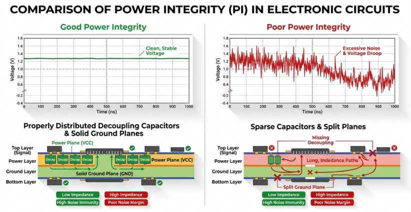
Transient load: When a processor or FPGA changes state, a spike of current is required, which causes voltage droop. At that frequency, if the PDN impedance is too high, the supply voltage drops below the minimum allowed operating voltage, which may result in a logic error or reset.
Excessive power supply noise: High-frequency switching noise gets into the power planes and radiates to critical analog circuits. This is particularly detrimental in mixed-signal applications where ADCs and DACs are on the same power rails as digital logic.
Ground bounce: Transient voltage differences across the ground network due to insufficient return path continuity or inadequate ground plane design corrupt the signal references.
EMI: Noisy PDN radiates electromagnetic energy from power planes, traces, and even decoupling capacitor loops. Many of the FCC Part 15 or CISPR 32 limit failures are really PDN problems.
Key Principles of Effective PDN Design
Power Plane Configuration and Decoupling Strategies
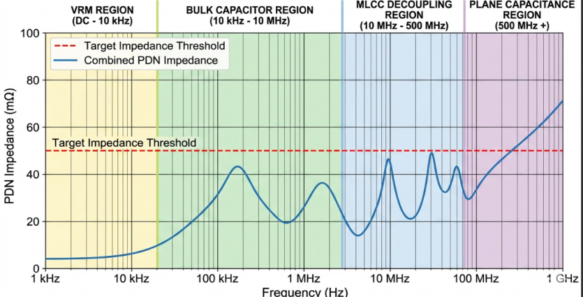
The voltage regulator module regulates the impedance at the lowest frequencies (DC up to a few kHz). The response speed of its output capacitance and feedback loop bandwidth, which is how quickly it can respond to load changes. Bulk decoupling capacitors assume the load in the mid-frequency region (100 kHz to 10 MHz) or so. Usually, they are ceramic or tantalum capacitors ranging from 10 uF to 100 uF located close to the VRM output. High frequency (10MHz to a few hundred MHz) is dominated by high-frequency ceramic decoupling capacitors. Here are the 100nF and 10nF MLCCs, which are as close as possible to the IC power pins. Their role is to provide immediate charge in transients, where the switching is quick.
Beyond a few hundred MHz, the power and ground plane pair is a distributed capacitor.
Capacitance of a pair of planes: C_planes = (E_r x E_0 x A) / d
The above quantities are the dielectric constant Er, the permittivity of free space E0, the overlap area A, and the dielectric spacing between planes d. This built-in capacitance is significantly increased by a tighter plane spacing (for example, 4 mil vs 8 mil prepreg between power and ground) and also reduces high-frequency impedance.
| Frequency Range | Primary PDN Element | Typical Values | Response Speed |
|---|---|---|---|
| DC - 10 kHz | VRM / Regulator | Feedback BW 10-100 kHz | Slowest |
| 10 kHz - 10 MHz | Bulk capacitors | 10 uF - 100 uF | Moderate |
| 10 MHz - 500 MHz | MLCC decoupling caps | 100 nF - 10 nF | Fast |
| 500 MHz+ | Power/Ground plane pair | Depends on geometry | Fastest |
Impedance Control and Voltage Drop Management
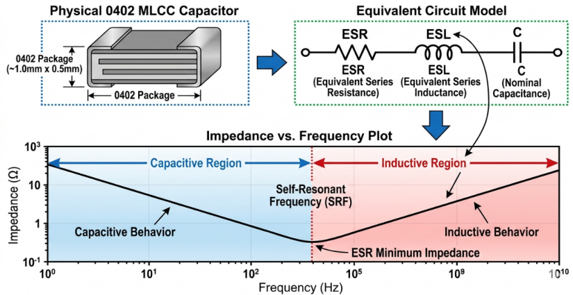
A common error is the selection of only the nominal capacitance of the decoupling capacitors. All capacitors also contain parasitic equivalent series resistance (ESR) and equivalent series inductance (ESL) that set the frequency range that they can be used within. A 100 nF 0402 size MLCC may have ESL of 0.5 nH and ESR of 10 milliohms. The upper limit of effectiveness is its self-resonant frequency (SRF), which is the frequency at which it switches from capacitive to inductive.
SRF = 1 / (2 x pi x sqrt(L_esl x C))
The SRF for that 100 nF cap with ESL (0.5 nH) is around 22 MHz. The capacitor acts as an inductor, and the impedance increases above this frequency. This is why several different values of capacitances are needed; each will provide coverage for a portion of the spectrum. A rough guideline: With a 1.0V rail, the total DC path resistance from VRM to IC should be less than or equal to 10-15 milliohms per ampere of current. The same rules apply for 3.3V rails, but there is more headroom.
Best Practices for PDN Design in PCB Layout
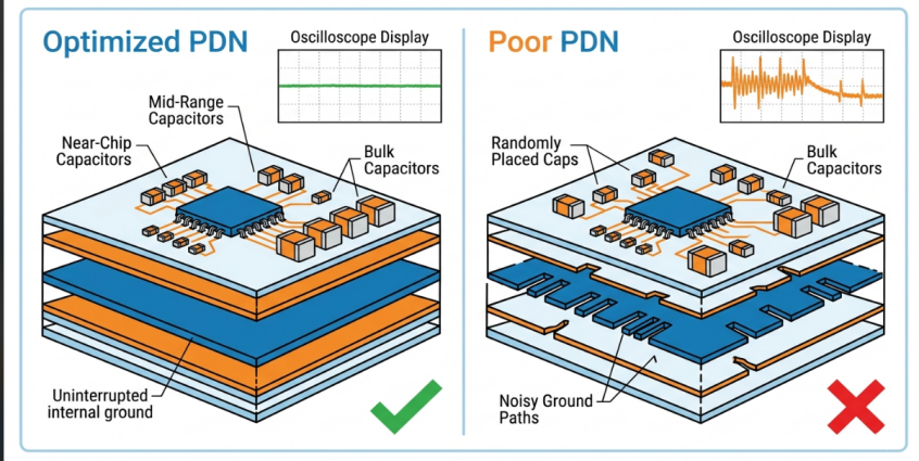
Capacitor Placement and Loop Area Minimization
Decoupling capacitors are as critical to their value as to their physical location. The objective is straightforward: The current loop area between the capacitor, IC power pin, and return path through the ground plane needs to be minimized. Each current loop is an inductor, and the inductance is proportional to the enclosed area. A decoupling capacitor that is 10 mm from an IC power pin with vias that route through multiple layers will form a much larger loop and thus have much more parasitic inductance than a capacitor that is 1 mm from an IC power pin with direct vias (vias that drop straight to the nearest plane pair).
These are placement rules for achieving the best PDN performance:
- Capacitors (10 nF, 100 nF) with high frequency should be placed near IC power pins, preferably within 1-2 mm, on BGA packages. They should be placed on the opposite side of the board from the power pin cluster.
- Use via-in-pad or adjacent vias to connect capacitor pads directly to the power and ground planes. Each mm of trace between the capacitor pad and the via increases the inductance.
- Capacitors (1 uF, 10 uF) of mid-range should be kept within 5-10 mm of the IC. These don't have to be as close as these are running at lower frequencies, where inductance is not as important.
- Use bulk capacitors (22 uF - 100 uF) close to the VRM output. They are primarily used for energy storage by the regulator, not high-frequency decoupling.
Layer Stackup Optimization for PDN Performance
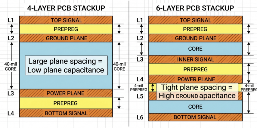
The most important decision you make to achieve PDN performance is your layer stackup, and you must get this right before you route a single trace. Power and ground plane placement, spacing, and stacking order have a direct impact on the high-frequency impedance of your PDN. For a typical 4-layer board, the recommended PDN-optimized stackup is:
| Layer | Function | Typical Thickness |
|---|---|---|
| L1 | Signal + Power pour | 1.2 mil copper (1 oz) |
| Prepreg | Dielectric | 7-8 mil |
| L2 | Ground plane (solid) | 1.2 mil copper (1 oz) |
| Core | Dielectric | 40 mil |
| L3 | Power plane (solid) | 1.2 mil copper (1 oz) |
| Prepreg | Dielectric | 7-8 mil |
| L4 | Signal + Ground pour | 1.2 mil copper (1 oz) |
For a 6-layer PDN-optimized stackup:
| Layer | Function | Spacing to Next Layer |
|---|---|---|
| L1 | Signal | 5 mil prepreg |
| L2 | Ground plane | 4 mil prepreg |
| L3 | Signal / Power | 20 mil core |
| L4 | Power plane | 4 mil prepreg |
| L5 | Ground plane | 5 mil prepreg |
| L6 | Signal | -- |
The L4-L5 power-ground pair (4 mil spacing) is tightly coupled and offers very good high-frequency decoupling. Some of the more advanced designs can go even further and reduce this gap to 2-3 mil with thin prepreg layers such as 1080 or 106 glass styles.
Manufacturing Considerations for Robust PDN Implementation
Plane Copper Thickness and Etching Uniformity
Creating an excellent PDN on screen is only half the job done. The fabrication process should closely represent your design intent, and there are a number of manufacturing variables that directly influence PDN performance. The number one way to control the DC resistance is by changing the copper weight. Most signal layers can get by with 1 oz copper (1.2 mil / 35 um thick), but power planes with lots of copper flowing through them will benefit from 2 oz (2.4 mil / 70 um thick) or even 3 oz copper. Copper Plane DC resistance is inversely proportional to thickness; increasing the copper weight by a factor of 2 will decrease the resistance by a factor of 2.
But the use of heavier copper presents manufacturing compromises:
Etching: Lateral undercutting is greater as the copper is thicker, and etch times are longer. This decreases the accuracy of the trace width and the minimum feature sizes. A 4 mil trace pattern on 1oz copper might require 5-6mil on 2oz copper to obtain the same final width.
Lamination: Thicker copper needs more prepreg resin fill, particularly in the area around the dense trace pattern. Voids or delamination may result from insufficient resin.
Drilling: Greater Cu content, which causes increased wear on the drills, may result in burring around the hole walls, which could impact reliability per IPC-6012 Class 2 and 3 requirements.
JLCPCB's Expertise in PDN Design and Fabrication
Advanced Support for Complex PDN Layouts and DFM
Creating a good PDN design demands a manufacturer with a solid understanding of the engineering behind your decisions. JLCPCB offers a full DFM (Design for Manufacturability) review, which detects potential PDN problems before they get to manufacturing.
Plane clearance, copper balance, via configurations, and stackup feasibility are part of their standard order process that their engineering team reviews. The DFM review ensures that your design requirements that call for a tight spacing between the power-ground planes to maximize PDN capacitance or 2 oz copper to achieve low-resistance power distribution are feasible with their process.
Reliable Production from Prototype to Volume
PDN design validation doesn't stop at the prototype stage. Consistency is the most important thing in going from prototype to volume production. If a PDN is excellent on the first batch, it has to be exactly the same on the thousandth batch.
To ensure this consistency, JLCPCB has established standardized processes, incoming material inspection, in-process monitoring, and final quality control according to the IPC-A-600 Class 2 standard. They also have SMT assembly services for the precise placement of decoupling capacitors, such as 0201 packages. The high precision of fabrication, comprehensive DFM review, and steady volume production offer a strong manufacturing base for the engineers who are developing how to design PDN networks to be reliable at scale.
FAQ about PDN Design
Q: What is PDN design in PCB design?
PDN design (Power Distribution Network design) is the process of engineering the complete power delivery path from voltage regulators to IC power pins on a PCB. It encompasses power plane configuration, decoupling capacitor selection and placement, via design, and layer stackup optimization.
Q: How do I calculate target impedance for my PDN?
Use the formula Z_target = V_ripple / I_transient. Determine the maximum allowable voltage ripple on your power rail (typically 3-5% of the nominal voltage) and the maximum transient current your ICs will draw.
Q: How many decoupling capacitors do I need?
There is no universal number. The quantity depends on your target impedance, the frequency range you need to cover, and the transient current demands of your ICs. Start with the IC manufacturer's recommendations, then use PDN simulation tools to verify that your capacitor network meets the target impedance across the full frequency band.
Q: What tools can I use to simulate PDN impedance?
Several commercial tools offer PDN simulation, including Ansys SIwave, Cadence Sigrity PowerDC and OptimizePI, Keysight PathWave ADS, and Altium PDN Analyzer. For simpler designs, spreadsheet-based calculators that model capacitor networks with ESR and ESL values can provide useful first-order analysis.
Conclusion
A well-designed Power Distribution Network (PDN) is the foundation of any reliable, high-performance PCB. While signal integrity often receives more attention, it is the PDN that ultimately determines whether your FPGA boots successfully, your ADC delivers clean data, or your high-speed interfaces run without errors.
By carefully calculating target impedance, strategically placing decoupling capacitors, optimizing layer stackup for tight power-ground plane coupling, and selecting appropriate copper weights, you can deliver stable, low-noise power across a wide frequency range. These practices not only prevent common issues like voltage droop, ground bounce, and EMI, but also improve overall system reliability and first-pass success rates.
Ultimately, great PDN design is a combination of sound engineering principles and high-quality manufacturing execution. Partnering with an experienced manufacturer like JLCPCB — with strong DFM support, consistent fabrication processes, and advanced capabilities in stackup, via-in-pad, and heavy copper — ensures your design translates perfectly from simulation to volume production.
Keep Learning
How Modular PCB Design Simplifies Complex Electronics Projects
Key Takeaway Modular PCB design simplifies complex electronics by breaking boards into independent, reusable functional blocks with clear interfaces. It boosts reusability, speeds up debugging, enhances team collaboration, and reduces errors.Shift from flat to modular design for faster development and more scalable, reliable PCBs. Ever seen a 400+ component schematic and got your head scrambled before even beginning routing? You are not alone. With the ever-increasing density of electronics combined w......
Your Ultimate Guide to PCB Rulers
In the world of PCB design and manufacturing, having the right tools is crucial for achieving accuracy and precision. One such tool that has gained popularity among professionals and hobbyists is the PCB ruler. This specialized measuring tool is designed to provide accurate measurements, reference information, and component footprints, assisting designers, engineers, technicians, and assemblers in various stages of PCB development. In this guide, we'll explore what a PCB ruler is, the features and mea......
Understanding the Materials Used in PCBs: Selection, Types, and Importance
Key Takeaways FR-4 is the go-to material for most cost-effective and reliable PCBs. Use Rogers for high-frequency and RF applications to reduce signal loss. Higher copper weight (2oz) improves current and heat handling. Choose High-Tg substrates for better thermal stability in multilayer boards. Green LPI soldermask offers the best balance of performance and inspection. Printed circuit boards (PCBs) are an essential component of modern electronics. These boards connect and support electronic component......
How to Select Tg of PCB ?
What is the Tg of PCB? In PCB manufacturing, "Tg" stands for Glass Transition Temperature. It is the temperature at which the PCB substrate material transitions from a rigid, glassy state to a soft, rubbery state. PCBs are flame-retardant (UL94 V-0) and do not burn easily; instead, they soften above Tg. The Critical Correlation Between Tg and Z-Axis CTE (Coefficient of Thermal Expansion) When the temperature exceeds the Tg point, the PCB substrate material (such as standard FR-4) undergoes a physical ......
How to Choose the Thickness of PCB
First, In the world of electronic products, the PCB is often referred to as the "heart" of the device. It interconnects all components, making board thickness one of the most important parameters. Choosing the right PCB thickness directly affects the electrical performance, mechanical stability, thermal management, and long-term reliability of the final electronic product. The process of selecting PCB thickness is influenced by various factors, such as product application scenarios, board material, an......
PCB Copper Pour Basics
What is Copper Pour in PCB Design? Copper pour refers to the technique of filling unused areas of a PCB's copper layers with solid copper planes. These planes are connected to power or ground nets, creating a continuous conductive path. Copper pour is typically used in the power and ground planes, as well as in signal layers for specific purposes. Purpose and Benefits of Copper Pour: Copper pour is primarily used to fill unused areas on PCB copper layers with solid (or hatched) copper connected to pow......