The Critical Role of Copper Peel Strength in Durable PCB Performance
12 min
- Understanding Copper Peel Strength
- Why Copper Peel Strength Is a Key Indicator of PCB Reliability
- Factors That Influence Copper Peel Strength
- Design and Manufacturing Strategies to Maximize Peel Strength
- Common Peel Strength Issues and Prevention Methods
- JLCPCB's Expertise in High Peel Strength PCB Production
- FAQ about Copper Peel Strength
- Conclusion
Key Takeaways
- Standard Test: Measured via the IPC-TM-650 90° pull test in N/mm.
- Core Function: Prevents pad lifting and delamination under thermal stress and CTE mismatch.
- Foil Types: ED foil provides higher adhesion; RA foil yields lower signal loss.
- Material Benchmarks: Standard FR4 averages 1.0–1.4 N/mm, while High-Tg FR4 achieves 1.2–1.6 N/mm.
- Design Tips: Add teardrops, eliminate unsupported copper slivers, and perform DFM checks.
Ever wonder what's making the copper stay put on your circuit board? It's not glue (in the usual sense of the word), and it's not magic. The answer is Copper Peel Strength, the strength of the bond between the copper foil and the laminate that is under the foil. The thing is, all traces, pads, and planes rely on that bond to maintain their strength over reflow, thermal cycles, and years of service.
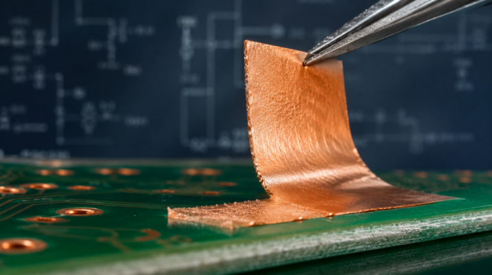
If the peel strength is high, your board will withstand thermal stress. It's when it's low that you receive lifted pads, broken joints, and delamination that quietly doom an otherwise flawless design. On this day, we will be discussing what Copper Peel Strength actually is, how it is compared to IPC standards, what things increase or decrease the strength of the copper adhesions, and how to design and manufacture for good Copper Peel Strength. Let's dig in.
Understanding Copper Peel Strength
What Copper Peel Strength Is and How It Is Measured
So, what does Copper Peel Strength really mean? The force needed to remove a piece of copper foil from the insulating material it is bonded to per unit width. It is measured in newtons per millimeter (N/mm) or sometimes pounds per inch (1 N/mm = 5.71 lb/in). The 90-degree peel test, a standard industry test, is IPC-TM-650 Method 2.4.8. A known-width copper trace is pulled at a constant angle away from the laminate surface, and the pull on the trace is measured by a load cell. The math is simple:
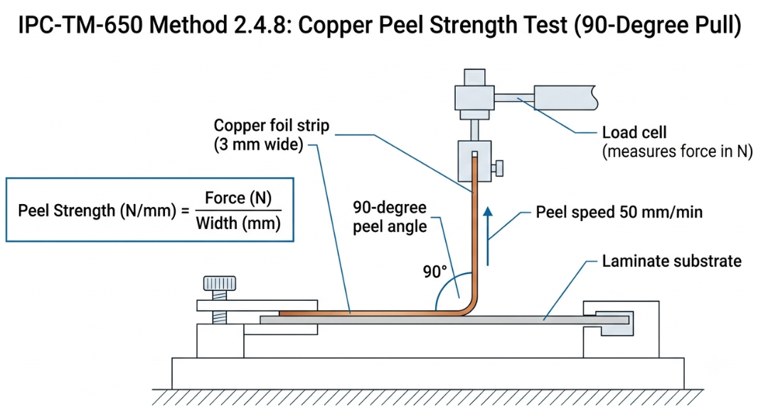
Peel Strength (N/mm) = Peel Force (N) ÷ Sample Width (mm)
Typical test parameters look like this:
- The specimen must be at least 3 mm wide and at least 75 mm long after peeling.
- The peel is peeled at a constant velocity of 50 mm/min.
- Storage: 35 °C and 75 ° C relative humidity
- Intervals: 1000ms between steps; 1500ms between sets; 3000ms between series
Industry Standards and Typical Values for Different Materials
Baked into the material specs are the peel strength requirements. The laminate and prepreg requirements are specified in IPC-4101, and the finished rigid board in IPC-6012. These minimum peel values are standards that a qualified PCB material is required to have in each condition. Typical 90-degree peel strengths (as-received) for common substrates are presented in the table below for 1 oz electrodeposited copper foil. These are engineering reference points only; real values will vary, depending on foil grade and treatment.
| PCB Material | Typical Tg (°C) | As-Received Peel Strength (N/mm) | Notes |
|---|---|---|---|
| Standard FR4 | 130–140 | 1.0–1.4 | Baseline for most designs |
| High-Tg FR4 | 170–180 | 1.2–1.6 | Better thermal retention |
| Rigid Polyimide | 250+ | 0.9–1.3 | High-temp, aerospace grade |
| PTFE / Rogers (hydrocarbon-ceramic) | — | 0.8–1.2 | RF-optimized, lower roughness |
| Aluminum-base (MCPCB) | — | 1.0–1.5 | Dielectric-to-copper bond |
Why Copper Peel Strength Is a Key Indicator of PCB Reliability
Impact on Solder Joint Integrity and Thermal Stress Resistance
All solder joints exert a force on the pad below them. In reflow, the shear and peel forces occur directly at the solder-to-laminate interface, where there is a mismatch in CTE between the copper, laminate, and solder. In the case of weak bonding of copper foil used in the construction of PCBs, the interface fails before the solder. This leaves an elevated pad, which may appear good at first glance, but the copper has separated from the substrate. The high peel properties prevent the pad from being pulled up from the other component, allowing it to sustain the mechanical and thermal load as desired. This is particularly true for lead-free assembly, in which the reflow temperature of the SAC305 ranges between 245-250 °C and the laminate spends more time at temperatures near its glass transition temperature.
Relationship with Delamination Risks During Assembly and Operation
Delamination occurs when the layers within the board separate; for example, when the prepreg separates from the copper or when the prepreg separates from the core. Peel strength is a common domino effect: When a bond begins to break at some point under thermal stress, moisture, and multiple heat exposures, the crack propagates outward. Monitor for the following causes of delamination, which are directly related to poor bond strength to the copper:
- Blisters or bubbles following reflow/wave soldering.
- This woven glass cloth has been marred by measling and crazing.
- A problem that occurs with the plated through-hole is that the inner layers separate out, causing barrel cracks.
- Field failures due to thermal cycling for months.
A board with high peeling force is resistant to all these due to the increased resistance of the interface under the expansion and contraction of the laminate.
Factors That Influence Copper Peel Strength
Copper Foil Type, Surface Treatment, and Substrate Material
The biggest single factor is the copper foil. There are two main families:
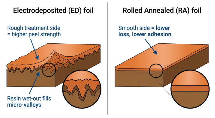
Electrodeposited (ED) foil: Developed using the electroplating method, and has a naturally rough matte surface. The roughness provides mechanical gripping with the resin, resulting in greater peel strength for less cost. It is the default for FR4.
Rolled annealed (RA): Mechanically rolled to a smooth, ductile finish. Because of the low roughness and consequently the low conductor loss, it is useful for flex circuits, as well as for applications with high frequency, while at the same time the smoothness may reduce the peel strength.
The treated side is the matte surface that is attached to the laminate; it is chemically roughened and is usually coated with a layer of nodular copper or black oxide that increases the adhesion. The resin system is also important: with good wet-out, the resin is able to flow into all the micro valleys in the foil and bestows the maximum surface contact.
FR4 and High-Performance Laminates: Peel Strength Comparison
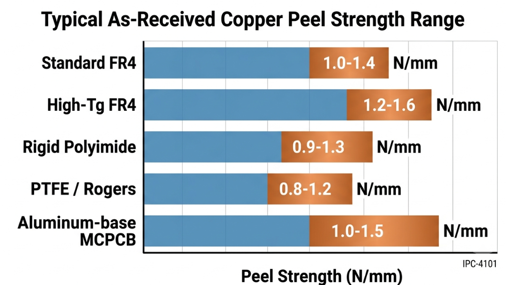
In mainstream electronics, standard ED foil with a mid-Tg resin has a good 1.0-1.4 N/mm, which is why most of the common electronics use FR4. High-Tg FR4 is able to push slightly higher and maintain that bond at high temperatures. But FR4 is not so for RF applications. PTFE and ceramic-filled hydrocarbon materials, such as Rogers grades, are developed to have properties of low dielectric loss, generally resulting in smoother foil and low peel properties. Designers embrace this compromise and make up for it with careful thermal and via design, and not simply aiming for raw adhesion numbers.
Design and Manufacturing Strategies to Maximize Peel Strength
Material Selection and Surface Preparation Best Practices
The most intelligent design strategy is to select a laminate that meets the thermal requirements. Consumer boards can use standard FR4, while high-Tg laminates, like Shengyi S1000-2 or KB-6160 class, are suitable for boards to withstand lead-free reflow or high ambient temperatures. Some best practices when putting this into practice are:
- Use the correct foil weight/strength for the current and thermal load; heavier copper requires a stronger bond to prevent lifting.
- Do not use slivers or thin, unsupported copper features that tend to peel off the board.
- Place teardrops at the point of contact between traces and pads to disperse mechanical stress.
- The surface must be kept clean; contamination and oxidation are enemies of adhesion.
Process Control in Lamination, Etching, and Surface Finish
Peel strength is the one that is won or lost in the manufacturing process during the lamination. The press needs to be preset to the correct temperature, pressure, and cure time for the resin to completely cure and flow into the foil treatment. A typical problem that leads to weak bonds is undercuring the resin. The risks of etching and surface finish further apply. Excessive etching or cleaning may undercut fine traces and reduce the thickness of the nodules that anchor the threads. A good controlled ENIG / HASL process will ensure the protection of the copper interface to the end product.
Common Peel Strength Issues and Prevention Methods
Root Causes of Low Peel Strength and Delamination
There are a handful of causes for most low-peel failures:
- Resin under-cured, from inadequate lamination pressure or temperature
- Excessive treatment or cleaning, which will remove the anchoring layer of foil
- Laminate or prepreg moisture absorption prior to pressing, which results in steam voids in reflow.
- Particles that are greater than this size at the bonding interface are contaminated.
- Slowly breaking a marginal bond with thermal cycling fatigue.
Each of these can cause a board to be drawn below its rating for peel strength, and more than one of these is frequently at work simultaneously.
Quality Testing and Verification Techniques
Without measurement, you can't manage! Reliable fabs do continual, not hope-for-the-best, peel strength checks. Combined, these techniques make it possible for the strength of the peel to be taken from a hopeful assumption to a documented result. Typical verification methods are:
- Peel testing of production coupons, in as-received and thermally stressed conditions (IPC-TM-650).
- Thermal stress testing (solder float / multiple reflow passes) to expose weak bonds.
- Cross-section microsectioning to view the copper to resin interface and plated through-hole barrels.
- Long-term durability under heat and humidity is modeled by HAST and thermal cycling.
- Automated Optical and X-ray inspection for detecting delamination, voids, and lifted features.
JLCPCB's Expertise in High Peel Strength PCB Production
Strict Material Qualification and Advanced Lamination Processes
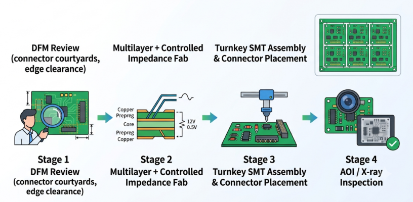
JLCPCB's laminate systems are qualified and take advantage of the laminate types offered by the suppliers, including standard FR4 or the higher Tg FR4 for use, with the laminate grade selected based on the IPC-4101 peel and thermal requirements. The incoming material of PCB is inspected for the copper foil and resin, so that they are matched and can be bonded reliably. Their lamination lines are tightly controlled, temperature, pressure, and cure profiles; controlling the peel strength is really where it begins. Consistent presses result in a more complete resin cover of the foil treatment, which leads to bonds that will withstand the lead-free reflow process.
Reliable Manufacturing with Consistent High Peel Strength Performance
All orders are automatically sent for a DFM check, screening for features that would likely peel away, especially at the copper interface, which would cause the most damage. JLCPCB ensures the consistent peel strength from prototype to volume with inline inspection, coupon testing, and repeatable process windows. As you are implementing these principles, they will be easily quoted and quickly prototyped, PCBs from as little as $2, to test a strong stackup before scaling.
FAQ about Copper Peel Strength
Q: What is a good Copper Peel Strength value for a standard FR4 PCB?
For a typical FR4 PCB with 1 oz electrodeposited copper, an as-received peel strength of roughly 1.0–1.4 N/mm is considered healthy. After thermal stress, it may drop toward 0.7 N/mm, which is still within IPC acceptance for most applications.
Q: How is Copper Peel Strength actually measured?
It is measured with the IPC-TM-650 Method 2.4.8 90-degree peel test, where a copper strip is pulled from the laminate at 50 mm/min while a load cell records the force. Peel strength equals the peel force divided by the strip width, reported in N/mm.
Q: Why does peel strength drop after soldering or thermal cycling?
Heat pushes the laminate near its glass transition temperature, where the resin softens, and the copper-to-resin bond weakens. Repeated cycling and moisture can then propagate small separations into full delamination.
Q: Does ED or RA copper foil give higher peel strength?
Electrodeposited (ED) foil generally gives higher peel strength because its rough matte side mechanically interlocks with the resin. Rolled annealed (RA) foil is smoother for lower high-frequency loss but tends to bond less aggressively.
Q: How can I improve copper adhesion in my design?
Choose a laminate qualified for your thermal profile, add teardrops at pad junctions, avoid isolated copper slivers, and match copper weight to the load. Then rely on a fabricator with controlled lamination and DFM checks to protect the bond.
Conclusion
While Copper Peel Strength may be just one line on a datasheet, it plays a crucial role in determining the success or failure of your board in the field. It relates directly to solder joint reliability, delamination resistance, and long-term reliability when soldered under thermal stress, and is worth attention long before you press the fabricate button.
The positive side of this is that you can fully control the adhesion of the strong copper. Select the appropriate PCB material for your temperature range requirements, understand the importance of the foil-resin team, and rely on a lamination and DFM expert. The demand for high power density, lead-free processes, and ever more sophisticated electronics will only increase the importance of having strong peel strength, and implementing this in the design phase is the best way to ensure long-lasting, high-quality electronics boards.

Keep Learning
How Copper Foil Shapes PCB Performance and Manufacturing Quality
Key Takeaways Weight: 1 oz copper ≈ 35 µm thickness; higher weight increases current capacity. Types: ED for standard rigid boards, RA for dynamic flex circuits. DFM & Loss: Smoother foil lowers RF loss; thicker foil requires wider trace spacing. The part of a PCB that actually carries the electrical signal is the copper foil. The strength comes from the glass weave, the resin is used to keep the layers together, and the solder mask is used to provide protection and separation of exposed copper. But w......
A Complete Guide to Copper Clad Laminate (CCL) in PCB Manufacturing
Key Takeaways CCL is the base material: a cured resin-reinforcement sheet with copper foil bonded to one or both sides. Three parts control performance: Resin affects heat and loss, reinforcement controls stability, and copper foil affects conductor behavior. Choose by the main design stress: Heat, frequency, and cost usually determine the best laminate family. Slash sheets define the material: IPC-4101 uses numbered slash sheets to specify rigid PCB base materials. Tg alone is not enough: Td and time......
Buried Vias in Advanced PCBs: Enabling Higher Density, Better Signal Integrity, and Compact Designs
Key Takeaways Hidden Routing: Buried vias connect only inner layers, keeping outer surfaces clear for dense components and traces. Better Signal Integrity: They eliminate via stubs, reducing parasitics and signal loss in high-speed designs. Higher Density: Essential for HDI boards, dense BGAs, and small form factors like wearables. Higher Cost: Sequential lamination and extra drilling steps make them ~3×-4× more expensive than standard through-holes. Ever wondered how a modern smartphone mainboard can......
Unlocking Higher Density and Better Performance with Blind Vias in HDI PCBs
Key Takeaway Higher Density: Connects surface to inner layers without penetrating the whole board, freeing routing channels under fine-pitch BGAs. Improved Signal Integrity: Reduces via stub length to minimize impedance discontinuities in high-speed designs. Aspect Ratio Rule: Keep the depth-to-diameter ratio near 0.75:1 (max 1:1) for reliable laser drilling and void-free plating. Thermal Efficiency: Supports via-in-pad setups for better heat dissipation and compact component placement. Ever wonder ho......
How to Select Tg of PCB ?
What is the Tg of PCB? In PCB manufacturing, "Tg" stands for Glass Transition Temperature. It is the temperature at which the PCB substrate material transitions from a rigid, glassy state to a soft, rubbery state. PCBs are flame-retardant (UL94 V-0) and do not burn easily; instead, they soften above Tg. The Critical Correlation Between Tg and Z-Axis CTE (Coefficient of Thermal Expansion) When the temperature exceeds the Tg point, the PCB substrate material (such as standard FR-4) undergoes a physical ......
Beyond the Basics: The Role of PTFE PCBs
Polytetrafluoroethylene (PTFE) PCBs are integral to advanced electronic applications. Among various PCB materials, Teflon, the brand name for Polytetrafluoroethylene (PTFE). Teflon PCBs, known for their high frequency and heat resistance properties. All of this is achievable due to its exceptional dielectric properties. RF PCB designs often make use of low-loss PTFE-based materials thanks to their very low dielectric losses and huge range of possible Dk values. Low Dielectric Constant: Enables high-sp......