Etched FPC: Manufacturing Process, Advantages, Applications, and Selection Guide
16 min
- What Is Etched FPC?
- Etched FPC Manufacturing Process Explained
- Etched FPC Design Considerations
- Advantages and Disadvantages of Etched FPC
- Etched FPC vs FDC: Which Technology Should You Choose?
- Applications of Etched FPC
- How to Select an Etched FPC Manufacturer?
- JLCPCB Etched FPC Manufacturing Capability
- Frequently Asked Questions (FAQ)
Ever noticed that thin, amber-coloured ribbon running between the boards in a smartphone camera module or a notebook's lid? That ribbon is almost surely an etched FPC, a flexible printed circuit that's created by chemically removing the unwanted copper to create a precise conductive pattern. It's one of the workhorses of modern electronics, and most people are unaware of the amount of engineering that goes into it.
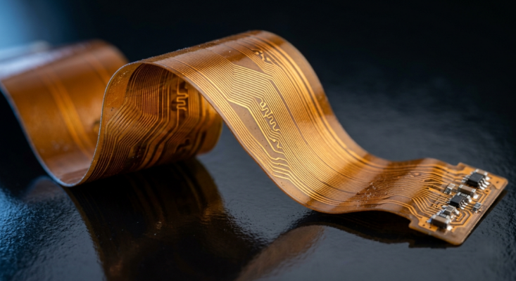
There are more than one flavor of flexible circuit, and the method of manufacture affects cost, precision, and reliability. The etched FPC is the high-precision one; it is what you grab when you need fine traces, multiple layers, or high signal speed in a bendable package. In this guide, we will explain what an etched FPC is, how the etching process works step by step, what the design rules are that you need to adhere to to ensure that your circuit is reliable, and what the differences are between etched FPCs and FDC (flexible die-cut circuits). Real-life examples will also be discussed, and a checklist for selecting a manufacturer will be provided. Let's get into it.
What Is Etched FPC?
Definition of Etched FPC
Etched FPC is a flexible printed circuit, which is made through a subtractive process (a sheet of copper bonded to a flexible film and then a chemical removes everything except the circuit). The base material is typically a flexible copper-clad laminate (FCCL) that is usually polyimide or polyester film with a thin layer of copper foil laminated onto it.
So why "etched"? This process consists of chemical etching (where exposed copper is dissolved in an acidic or alkaline solution). The basic principle used is the same as for rigid PCBs, except that it is used with thin flexible substrates. The end result is a circuit capable of bending thousands of times without causing any disruption to signals. Etched FPCs are single-sided, double-sided, and multilayer (1-8 layers) and cannot be achieved by mechanical means. It's the accuracy that makes it the preferred option for high-speed and high-density flexible use.
How Does the Etching Process Work in FPC Manufacturing?
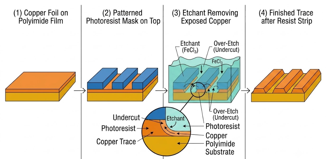
In fact, etching is a form of controlled corrosion. The copper surface to be protected is covered with a pattern, and the whole panel is placed in the etching machine, usually a spray etching chamber that sprays the surface with etchant. The chemistry and washing off attack the unprotected copper and leave the masked traces. Directional control is the main problem. The drawback of the etch is that it will not only wear away downward, but also sideways, or laterally, and that's called an undercut. This is managed by means of good process engineering (spray pressure, temperature, and timing). The smaller the traces, the more important the control of that chemistry.
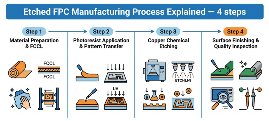
Etched FPC Manufacturing Process Explained
Step 1: Material Preparation and FCCL Selection
The most popular base is polyimide (PI) film, which is highly thermally stable at temperatures above 300°C and has excellent chemical resistance, and is bonded to a copper foil, usually 1/3 oz (12 µm), 1/2 oz (18 µm), or 1 oz (35 µm). The copper surface is first cleaned to remove dust, oils, and oxidation before imaging. This cleaning stage is not optional; even a fingerprint can cause resistance to come up and create an open circuit later. Typically, surface roughening or micro-etching and chemical cleaning are performed simultaneously. The copper foil type will also play a role here. Rolled-annealed (RA) copper is soft and easy to bend, and is commonly used for dynamic bend applications, while electrodeposited (ED) copper has a higher hardness and is used for static bending.
Step 2: Photoresist Application and Circuit Pattern Transfer
The light-sensitive photoresist is then coated, either as a liquid or more often as a dry film, which is laminated by heat and pressure. This layer will be what is left to protect your traces during the etch. Then the circuit pattern is transferred by using photolithography. A resist is exposed to UV light using a photomask (or a direct laser imager), which renders the resist harder in the spots that are supposed to be your copper traces. At the development stage, the unexposed resist is removed, exposing bare copper where you want it removed. This imaging step is the smallest feature you can make. The etched FPCs of today are capable of achieving tight tolerances, hitting traces as small as 20-30µm (about 0.8-1.2 mil) due to precise exposure and development.
Step 3: Copper Chemical Etching Process
Nowadays, the main actor of the show is. The developed panel goes into the etching tool, where the etchant will dissolve all the exposed copper. There are three chemistries that dominate the production of FPCs, and each has its own personality:
- Cupric Chloride (CuCl₂): Most popular etchant. Provides great stability, has a quick regeneration, and has clean fine lines in spray systems, which is the standard for high precision work.
- Ferric chloride (FeCl₃): Strong, aggressive acid etch chemistry, high etch rate, typically used for specialty films and higher thickness copper, but is more difficult to control and more difficult to regenerate.
- Ammoniacal (Alkaline) Etchant: This type of etchant is fast and is good for thicker copper, but it requires careful control of the pH and specific gravity to prevent changes.
Etch times are brief, typically 30 s to 3 min, depending on the thickness of the copper, the concentration of the etchants, and the temperature. The thinner the foil (9-18 µm thinner), the faster it will be cleared; the thicker the foil, the longer it will take. The parameter that engineers are watching is the etch factor: that is, the ratio between the depth of the etch and the lateral undercut. With a higher etch factor, leading to more vertical and precise sidewalls of the traces.
Step 4: Surface Finishing and Quality Inspection
The etching process then removes the resist, leaving a clean copper pattern behind. A coverlay (polyimide film with adhesive) or a flexible solder mask is then put over the circuit to protect the circuit and to delineate the exposed pads. Exposed pads need to have a surface finish so that the pads are solderable and won't corrode. Common options include:
- ENIG (Electroless Nickel Immersion Gold)
- OSP (Organic Solderability Preservative).
- Immersion tin or immersion silver
Lastly, the panel is examined. Automated Optical Inspection (AOI) detects width and spacing failures; electrical testing ensures opens and shorts are detected; mechanical bend or cyclic-flex testing ensures that the circuit endures in the real world. The outline is then punched (or laser cut) into shape.
Etched FPC Design Considerations
Material Selection: Polyimide vs Polyester
The top of the range is polyimide because it can withstand soldering temperatures, chemical resistance, and repeated flexes. Hence, it is used in almost all high-performance etched FPCs.
The cheaper option is polyester (PET). It is cheaper, and it is suitable for low-temperature/low-stress applications. It will not withstand reflow soldering, and its properties deteriorate more rapidly with heat.
PI is a safe bet if your board is used in SMT assembly or has to be subjected to higher temperatures.
Trace Width, Spacing, and Layer Stack-Up
Etching comes in handy for tracing geometry. Production etched FPCs can easily be produced with 75-100 μm (3-4 mil) traces and spaces on thin copper, and advanced processes can reduce to 20-30 μm (0.8-1.2 mil) for the most fine design. A good rule of thumb: The minimum line width achievable is proportional to the thickness of the copper. For fine lines, use thinner copper (9-18 µm). For current capacity, opt for heavier and loosen the trace rules. Stack-up is also dependent on the number of layers. Single- and double-sided FPCs remain thin and flexible, but multilayer constructions (up to 8 layers) provide a higher routing density at the expense of bendability. Minimize high-flex areas for as few layers as possible.
Bend Radius and Mechanical Reliability
The bend radius is a first-class design parameter for flex circuits; flex circuits fail where they are bent. A basic rule of thumb is that for static bending, about 6 times the total thickness is the minimum required bend radius, and for dynamic (repeated) bending, 10 times or greater is required. To prevent excessive fatigue, adhere to several guidelines:
- The route is always at a right angle to the bend line, Not at a diagonal across the line.
- Use a neutral bend axis for copper, balancing layers as much as possible.
- Do not have plated through-holes or component pads in the bend area.
- Avoid using sharp 90° trace corners – use curved (teardrop) trace corners.
- Stagger traces on alternate layers, not stacked.
These practices help maintain copper strain and greatly increase the number of flex cycles until a crack develops.
Advantages and Disadvantages of Etched FPC
Advantages of Etched FPC
Etched FPC is an established, proven technology, and its maturity has real advantages:
- The ability to route densely and complexly with fine features down to 20-30 µm.
- Multilayer support: 1 to 8 layers for sophisticated interconnects.
- Good signal integrity: Controlled impedance and clean geometry are appropriate for high-speed data.
- SMT compatibility: Allows soldering of components and connectors directly onto the flex.
- Dynamic flex durability: Withstands multiple flexing in hinges, cameras, and folding devices.
What Are the Disadvantages of Etching?
Not everything is ideal, and there are drawbacks to etching to plan for:
- Increased cost due to tooling and chemistry, particularly for prototypes and low volumes.
- Chemical handling of etchants such as cupric and ferric chloride needs special consideration for waste treatment and is not as environmentally friendly.
- The more steps, the more defects that can occur.
- The defects caused by the etching process, such as undercut and over-etching.
Etched FPC vs FDC: Which Technology Should You Choose?
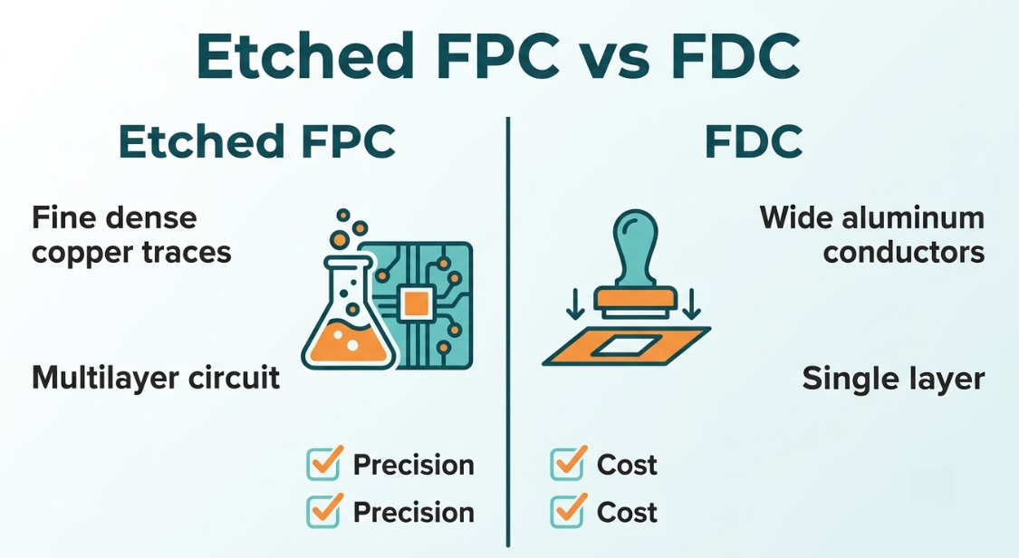
Understanding the other option is a good idea before making a decision. Flexible Die-Cut circuit is the acronym for Flexible Die-Cut circuit, which is a flexible conductor (usually aluminum or copper foil on PI) that is mechanically stamped to shape by a cutting die rather than being chemically etched. Precision cutting and lamination without the need for any photoresist or etchant.
Etched FPC vs FDC Comparison Table
| Parameter | Etched FPC | FDC (Flexible Die-Cut) |
| Circuit formation | Chemical (metal etching) | Mechanical die-cutting |
| Layer count | 1 to 8 layers | Single layer |
| Min trace/space | 20–100 µm (fine) | Wide conductors only |
| Conductor material | Copper (RA/ED) | Aluminum or copper foil |
| Circuit complexity | High, fine-pitch | Simple, low-density |
| SMT components | Fully supported | Limited / not typical |
| Environmental impact | Chemical waste to treat | No etchant, cleaner |
| Relative cost | Higher | 1/3 of FPC in volume |
| Best for | Precision, high-speed, dense | Simple, cost-driven, single-layer |
When Should You Choose Etched FPC?
Choose etched FPC in the cases where precision and reliability are key to the project. For fine pitch traces, multiple layers, controlled impedance for high-speed signals, or SMT soldered components on the flex, there's only one way to do it,t and that's etching. It is also the right choice when the application requires demonstrated, long-term reliability – automotive, medical, and communications hardware, where failure in the field is not an option. The more you spend, the more you get, and the more confident you are in your capabilities.
When Should You Choose FDC?
Use FDC if the circuit is simple, single-layer, and cost is the primary consideration. For example, battery cell-connection systems (CCS) are systems that feature wide aluminum conductors that deliver current between cells without the need for fine routing. FDC is also better on the sustainability score as it avoids the use of etchant chemistry altogether. When using a single layer and coarse geometry, the circuit cost for FDC can be reduced by about one-third of an equivalent FPC.
Applications of Etched FPC
Consumer Electronics
This is FPC's home turf. They are found in camera modules, button flexes, and display connections in smartphones; in the hinges of laptops, and in tablets, as well as in foldable phones that are expected to last for tens of thousands of open-close cycles. This unique mix of thin profile, small pitch, and dynamic-flex durability is ideal for densely packed consumer devices. Today's thin, folding form factors would not be possible if there were no etched FPCs.
Automotive Electronics
Cars are harsh environments: heat, vibration, years of continuous service. Etched FPCs on polyimide handle it, and are used in dashboards, infotainment systems, LED lighting, sensor arrays, and control modules near the engine. They are suited for modern vehicle electronics with their reliability when subjected to thermal cycling and vibration, and the capacity to route complex signals through a constrained environment.
Medical Devices
When it comes to medical hardware, size and reliability are key. Etched FPCs are the only way to be able to implement circuits that are extremely small, flexible, and biocompatible-adjacent (i.e., without the use of plastic casings) in wearable monitors, hearing aids, endoscopic camera assemblies, and even implantable sensors. The track record of etched FPC is a huge advantage that takes over this space, owing to the fact that failure can be a serious issue.
Wearables and IoT Applications
Electronics have to be integrated into curved, moving, space-constrained enclosures, such as smartwatches, fitness bands, wireless earbuds, and IoT sensor nodes. Etched FPCs allow designers to route around batteries and to conform to organic shapes. As wearables continue to get smaller and more sensors are incorporated, the need for fine-pitch flexible interconnects continues to grow, and etched FPC is the workhorse of fine pitch.
How to Select an Etched FPC Manufacturer?
Manufacturing Capability and Quality Control
First, you need to start with raw ability, you can only build it from there. Ask for minimum trace/space size, number of layers, maximum layer thickness of copper, and tolerance for impedance control. Make sure they are capable of handling your stack-up: multilayer, rigid-flex, or fine pitch single layer. A shop that is used to 25 µm and regular 100 µm lines is different from a shop that is only used for 100 µm lines.
Reliability comes down to the details in process control. Identify manufacturers that follow pertinent IPC Requirements – IPC-6013 (qualification and performance of flexible circuits) and IPC-A-600 (board acceptability). Look at their inspection stack as well: AOI, electrical (open/short), and mechanical flex testing. The certifications, including ISO 9001 or ISO 13485 in the medical field, or IATF 16949 in the automotive industry, are signs that the quality system is in place.
Prototype and Mass Production Support
Lastly, ensure that the partner can develop together with you. The ideal manufacturer has the ability to make fast, cheap prototyping, and then scale the same process to the volume without redesign. Some items to check:
- Fast turn prototype lead times and transparent pricing.
- A seamless transition from prototype to production on the same line.
- Get design-for-manufacturing (DFM) feedback prior to committing to tooling.
- Component sourcing and assembly, if required.
JLCPCB Etched FPC Manufacturing Capability
Advanced Etching Technology and Precision Manufacturing
Controlled etching is crucial for modern flexible-circuit fabrication, and the FPC lines at JLCPCB utilize precision spray etching to achieve fine trace geometry and uniform etch factor throughout the panel. It is that control that allows sidewalls to remain straight and which produces high on tight designs. This ensures reliable fine-line flexible circuits on polyimide with surface finishes such as ENIG and OSP that keep your pads solderable and reliable.
Flexible PCB Prototype and Mass Production Services with DFM Support
JLCPCB's flexible PCB service allows you to easily get from a first prototype to a production run without having to change vendors based on the implementation of these principles. Quick turnaround and instant online quoting mean early iterations are low-cost and quick to turn. Since the same is scalable, the flex you're building and testing as a prototype is the same flex you're shipping in volume, so there's a lot less risk in the transition!
The automated DFM checks, along with electrical testing and AOI provided by JLCPCB, can help identify problems early on, which is great for flex design. That includes warnings for bend-zone faults, spacing violations, and open/short faults in front. This learning feedback cycle is one of the quickest ways for a designer to learn what an actual, printable, manufactured, etched FPC will actually look like.

Frequently Asked Questions (FAQ)
What is etched FPC?
An etched FPC is a flexible printed circuit whose copper traces are formed by chemically dissolving away unwanted copper from a flexible copper-clad laminate. The base is usually polyimide or polyester film with copper foil, patterned using photoresist and etchant.
What is the difference between etched FPC and FDC?
Etched FPC forms circuits by chemical etching, supporting fine traces, multiple layers, and SMT components. FDC (Flexible Die-Cut circuit) forms conductors by mechanically stamping foil with a cutting die, limiting it to simple, single-layer designs.
What liquid is used for FPC etching?
The most common etchant is cupric chloride, valued for stability and clean fine-line results in spray systems. Ferric chloride is a stronger acid etching option for specialty films and thicker copper, while ammoniacal (alkaline) etchant suits fast etching of heavy copper.
How long does FPC etching take?
The etching step itself is fast, typically 30 seconds to 3 minutes. The exact time depends on copper thickness, etchant concentration, and bath temperature, with thin 9–18 µm copper clearing much faster than heavy foil.
What are common problems in FPC etching?
The classic defects are undercut (etchant eating sideways under the resist), over-etching (rough, narrowed traces), and under-etching (copper residue left behind). Uneven copper thickness also causes uneven etching across the panel.

Keep Learning
How Copper Foil Shapes PCB Performance and Manufacturing Quality
Key Takeaways Weight: 1 oz copper ≈ 35 µm thickness; higher weight increases current capacity. Types: ED for standard rigid boards, RA for dynamic flex circuits. DFM & Loss: Smoother foil lowers RF loss; thicker foil requires wider trace spacing. The part of a PCB that actually carries the electrical signal is the copper foil. The strength comes from the glass weave, the resin is used to keep the layers together, and the solder mask is used to provide protection and separation of exposed copper. But w......
A Complete Guide to Copper Clad Laminate (CCL) in PCB Manufacturing
Key Takeaways CCL is the base material: a cured resin-reinforcement sheet with copper foil bonded to one or both sides. Three parts control performance: Resin affects heat and loss, reinforcement controls stability, and copper foil affects conductor behavior. Choose by the main design stress: Heat, frequency, and cost usually determine the best laminate family. Slash sheets define the material: IPC-4101 uses numbered slash sheets to specify rigid PCB base materials. Tg alone is not enough: Td and time......
Buried Vias in Advanced PCBs: Enabling Higher Density, Better Signal Integrity, and Compact Designs
Key Takeaways Hidden Routing: Buried vias connect only inner layers, keeping outer surfaces clear for dense components and traces. Better Signal Integrity: They eliminate via stubs, reducing parasitics and signal loss in high-speed designs. Higher Density: Essential for HDI boards, dense BGAs, and small form factors like wearables. Higher Cost: Sequential lamination and extra drilling steps make them ~3×-4× more expensive than standard through-holes. Ever wondered how a modern smartphone mainboard can......
Unlocking Higher Density and Better Performance with Blind Vias in HDI PCBs
Key Takeaway Higher Density: Connects surface to inner layers without penetrating the whole board, freeing routing channels under fine-pitch BGAs. Improved Signal Integrity: Reduces via stub length to minimize impedance discontinuities in high-speed designs. Aspect Ratio Rule: Keep the depth-to-diameter ratio near 0.75:1 (max 1:1) for reliable laser drilling and void-free plating. Thermal Efficiency: Supports via-in-pad setups for better heat dissipation and compact component placement. Ever wonder ho......
How to Select Tg of PCB ?
What is the Tg of PCB? In PCB manufacturing, "Tg" stands for Glass Transition Temperature. It is the temperature at which the PCB substrate material transitions from a rigid, glassy state to a soft, rubbery state. PCBs are flame-retardant (UL94 V-0) and do not burn easily; instead, they soften above Tg. The Critical Correlation Between Tg and Z-Axis CTE (Coefficient of Thermal Expansion) When the temperature exceeds the Tg point, the PCB substrate material (such as standard FR-4) undergoes a physical ......
Beyond the Basics: The Role of PTFE PCBs
Polytetrafluoroethylene (PTFE) PCBs are integral to advanced electronic applications. Among various PCB materials, Teflon, the brand name for Polytetrafluoroethylene (PTFE). Teflon PCBs, known for their high frequency and heat resistance properties. All of this is achievable due to its exceptional dielectric properties. RF PCB designs often make use of low-loss PTFE-based materials thanks to their very low dielectric losses and huge range of possible Dk values. Low Dielectric Constant: Enables high-sp......