Why PCB Test Coupons Are Critical for Reliable Board Manufacturing
18 min
- The Role of Test Coupons in Quality Assurance
- Panel Layout and Structural Alignment
- Evaluating PCB Test Coupons: Advantages and Limitations
- Converting Test Data into Manufacturing Yield
- JLCPCB's Precision Coupon Testing Infrastructure
- FAQs about PCB Test Coupon
- Conclusion
Key Takeaways
- Sacrificial Testing: Coupons allow destructive tests without harming active boards.
- True Process Mirror: They match the exact stackup and density to reflect panel quality.
- Clean Measurements: Straight lines enable precise TDR impedance and via inspection.
- Quality Shield: Coupon failures isolate flawed panels before shipping.
A PCB test coupon is the one piece of your order that is intentionally destroyed. It rides in the panel border beside your boards, so it sees every drill, plating, and lamination step they do. Then it gets snapped off and sliced in half. It sounds wasteful, but it stands in for something you cannot otherwise reach. Almost everything that decides whether a board survives is buried inside it. The copper on a hole wall, the alignment of the inner layers, the true shape of a trace after etching: none of it is visible from outside.
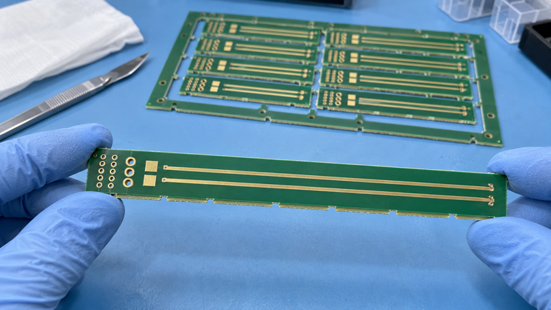
Figure 1: Impedance test coupon strip beside the production panel it came from
Once you see a coupon as a sacrificial copy rather than scrap, the quality report shipped with your boards starts to make sense. This guide covers what a coupon includes, where it belongs on the panel, which IPC coupon types measure, and where its verdict stops being trustworthy.
The Role of Test Coupons in Quality Assurance
A finished PCB hides almost everything that decides whether it lasts. Quality assurance, therefore, leans on a sacrificial stand-in that can be cut open, cooked, and pulled apart without costing you a board.
What Is a PCB Test Coupon?
A PCB test coupon is a small non-functional block of copper and laminate, built into the panel beside your boards. It is drilled, plated, laminated, and finished in the same passes they are. Whatever the process did to your copper, it did to the coupon as well, because both went through together. Nothing on it connects to your circuit.
A coupon carries rows of plated holes, long straight impedance lines, comb patterns for insulation tests, and bare copper strips for peel testing. Because no feature has to fit a component, each one can be sized for the instrument that will read it. Your fabrication notes can then call out a coupon type rather than describe a drawing.
| Coupon Type | What It Carries | What It Proves | When Your Order Needs It |
|---|---|---|---|
| A/B | Two rows of plated holes, component holes near 1.9 mm (75 mil) beside the smallest vias | Hole wall copper, layer registration, survival of reflow | Any multilayer board |
| D | Daisy chains of vias wired for a four-wire resistance reading | Interconnect resistance drift under thermal cycling | Class 3, HDI, and microvia stackups |
| Z | Single-ended and differential lines around 150 mm (5.9 in) long | Characteristic impedance measured by TDR | Any controlled-impedance order |
| P | A bare copper strip at least 3 mm (118 mil) wide | Foil peel strength and adhesion after heat | New laminates and heavy copper builds |
| E and H | Interdigitated comb patterns | Moisture resistance and surface insulation resistance | High-voltage or humid-environment boards |
| S | Plain pads and holes with no solder mask | Solderability of the surface finish | Long shelf life or aged stock |
Limitations of Testing Traces Directly on Production Boards
Most of the checks that matter are destructive, so running them on a shipped board is not an option. Measuring a hole in the wall copper means cutting the board in half and polishing the cut face. Pulling a peel strength figure means tearing copper off the laminate. Neither leaves you with a product. Non-destructive tests fail for a different reason: they answer a much narrower question. A flying probe confirms every net is connected and nothing shorts, and that is genuinely useful. But it says nothing about how thick the copper in a barrel is, or whether that barrel will crack on the third reflow.
Impedance is the awkward case, because you can measure it on a real trace, but the answer gets noisy. Production traces are short; they turn corners, change layers via vias, and run alongside other copper. A TDR sees all of that at once, so the flat region you need to average across may not exist. An impedance coupon wants a straight run of roughly 150 mm (5.9 in) to give a clean measurement window. A 40 mm (1.6 in) square sensor board has nowhere to put one, which is why impedance control is verified on the border rather than on the board.
Panel Layout and Structural Alignment
Strategic Location of Test Coupons Across Panels
A production panel is not uniform, which is the whole reason coupon position matters. Plating current density runs higher at the panel edges and corners, so copper builds up thicker there. Etchant spray hits the middle differently from the border. Resin also flows further under pressure where the copper coverage is light. A single coupon in one corner therefore reports that corner and nothing else. Common practice is at least two coupons per panel, placed at opposite ends and within about 25 mm (1 in) of the edge.
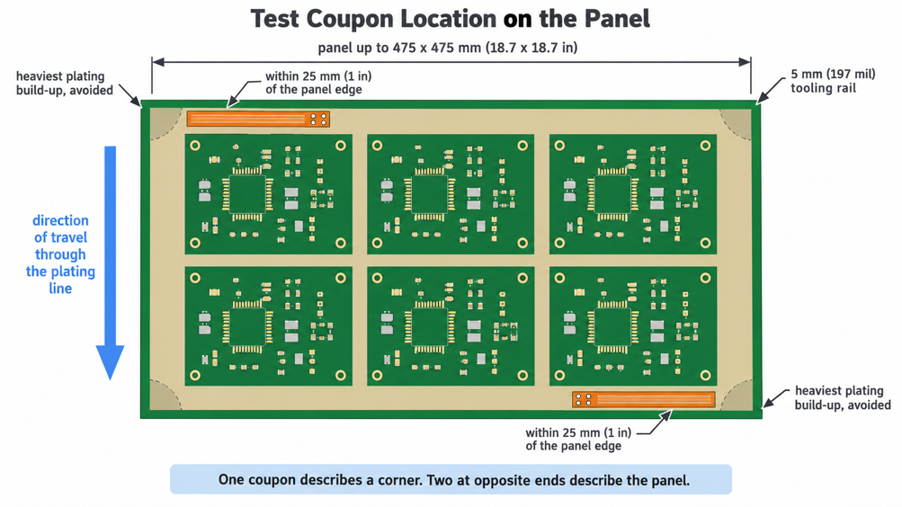
Figure 2: Panel top view showing coupon placement in the border rail at opposite ends
Coupons are aligned with the direction the panel travels through the plating line. A gradient along that axis then shows up as a difference between the two readings. Microsection coupons get sectioned in opposite directions for the same reason, which catches drill wander and registration shift in both axes. Physically, the coupons live in the breakaway rail, the strip of panel that gets routed away at the end. JLCPCB asks for 5 mm tooling edges on assembly orders, and coupon strips share that same border region.
Replicating Traces and Stackup Parameters Accurately
A coupon has to be a copy of your board, not a symbol of it. It uses the same stackup, the same copper weight, the same drill diameters, the same surface finish, and the same solder mask. If you change any one of those, the measurement stops applying to your product.
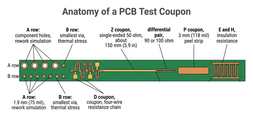
Figure 3: Anatomy of a combined A/B and impedance coupon
Impedance coupons need one line per controlled geometry rather than one line per board. Suppose you specify 90 ohm differential on layer 1 and 50 ohm single-ended on layer 4. The coupon then carries both, tested separately, because a single averaged number would hide whichever layer drifted.
- Layer stackup and pressed dielectric heights, because impedance and registration both depend on where the copper actually ended up after lamination.
- Copper weight on every layer, since plating thickness and etch undercut both scale with it.
- The largest component hole and the smallest via, as plating throw falls off sharply with hole aspect ratio.
- Surface finish and solder mask, which pulls measured impedance on the outer-layer microstrip down by 1 to 3 ohms.
- Local copper density is an isolated feature in bare laminate plates, thicker than the same feature in a crowded area.
Copper density is an item designers rarely consider, and it bites hardest during pattern plating. Current concentrates on isolated features, so a coupon sitting alone in bare laminate plates is thicker than a board crowded with traces. Fabs add copper thieving around the coupon to even that out, which is why a coupon looks busier than it needs to be.
Evaluating PCB Test Coupons: Advantages and Limitations
Coupons buy real evidence, but they charge real panel area for it. Knowing where that evidence is strong and where it thins out is what stops you from over-trusting a passing report.
Primary Benefits for Impedance and Microsection Testing
Impedance measurement gets dramatically easier on a coupon because every source of noise has been designed out. The line is long, straight, and isolated, with generous probe pads at one end. Measurement uncertainty drops to roughly 1-2 ohms, within a tolerance band of ±10 %.
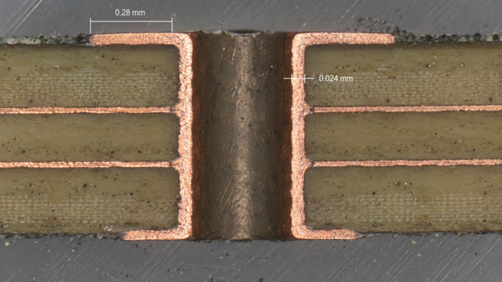
Figure 4: Microsection of a plated through-hole from an A/B coupon
Microsection testing is the other half, and it works only because the coupon is expendable. Cutting a coupon costs nothing you were going to ship, so the lab can drill as many holes as it needs to find the weak one.
- Cut the coupon out with a diamond saw through the row of holes to be examined.
- Mount the piece in clear epoxy so the cut face can be held flat and square.
- Grind through progressively finer silicon carbide papers, from 120 grit to 1200 grit.
- Polish the face down to roughly 0.05 µm so the copper boundaries stay sharp.
- Examine at 50x to 500x, then measure the hole wall copper, dielectric spacing, and annular ring.
That polished face shows the part of your board you can never otherwise inspect. Insufficient barrel plating, delamination, resin voids, drill smear, and cracks from thermal cycling all become visible once the copper boundaries are sharp. IPC-A-600 supplies the acceptability criteria, and PCB cross-section analysis walks through the full procedure.
Physical Constraints and Measurement Trade-offs
Panel area is the first cost, and it is not trivial. A 150 mm (5.9 in) impedance line, plus its ground structures, needs a strip of border that could otherwise hold boards on a small order that can push you into a lower boards-per-panel count.
The deeper limitation is that a coupon sits near your board rather than on it. It shares the panel, the bath, and the press cycle, so it represents all three well. It does not represent the specific sq-cm where your BGA lands, and etch varies measurably across a panel.
- Impedance results carry a similar gap: The coupon line is straight, isolated, and uniform, while your real trace turns corners, drops through vias, and runs beside neighbors. A coupon reading of 50 ohms is a statement about the process, not a promise about one particular net.
- Destructive tests are also one-shot: Once a coupon has been sectioned or peeled, it cannot be re-measured, so fabs section coupons in pairs. Dense HDI panels add their own problem, because there is often no border wide enough for a full-length impedance line.
| Aspect | What the Coupon Gives You | Where It Falls Short |
|---|---|---|
| Impedance | Clean TDR reading within 1 to 2 ohms, per IPC-TM-650 2.5.5.7 | A straight isolated line, so it does not model your routed net |
| Plating and copper | Direct microsection measurement of hole wall copper | Represents the panel, not the exact spot on your board |
| Thermal reliability | Reflow and shock cycling without risking the product | Destructive and one-shot, so an odd result cannot be repeated |
| Cost | Built by the fab with no design effort from you | Consumes the border area and can lower the boards per panel |
| Traceability | An archived record tied to the panel and batch ID | Only as useful as the fabrication notes that specified it |
Every row trades the same way, since the coupon wins on measurement quality and loses on locality. That is an easy trade to accept, as long as you never read a coupon result as a per-board guarantee. A coupon tells you what the process delivered across the panel. It does not tell you what happened at one pad on one board.
Converting Test Data into Manufacturing Yield
Numbers from a coupon are worth collecting only if they change something in the factory. Each measurement maps onto a specific process knob, and a threshold decides when that knob gets turned.
Key Metrics: Etch Rates, Copper Thickness, and Thermal Stress
Etch factor describes how much width a trace loses while the copper is being etched away. It is the copper thickness divided by the undercut on one side, so a higher number means a squarer trace. Typical production chemistry lands between 2.5 and 4.0, and fine-line work wants 3.5 or better. Working that through on 1 oz copper makes the consequence obvious. At 35 µm (1.4 mil) thick with an etch factor of 3.5, each side undercuts by about 10 µm. The trace loses roughly 20 µm (0.8 mil) in total, so a 200 µm line drawn in your layout arrives at about 180 µm.
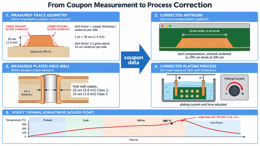
Figure 5: How coupon measurements feed back into etch compensation
Copper thickness carries the hardest numbers of the set. IPC-6012 sets a minimum average hole wall copper of 20 µm (0.8 mil) for Class 2 and 25 µm (1.0 mil) for Class 3. Microsection is the definitive measurement, while X-ray fluorescence gives a fast surface check to about 0.1 µm against those plating thickness targets.
Thermal stress testing asks a different question, which is whether the barrel survives assembly rather than whether it was built correctly. IPC-TM-650 method 2.6.8 floats the coupon on molten solder at 288 C for 10 seconds. Method 2.6.27 instead runs six reflow cycles at a 230, 245, or 260 C peak, which is much closer to a real lead-free profile.
| Metric | Coupon Used | Method | Typical Acceptance |
|---|---|---|---|
| Hole wall copper | A/B microsection | IPC-TM-650 2.1.1 | 20 µm (0.8 mil) Class 2, 25 µm (1.0 mil) Class 3 |
| Etch factor | A/B or a dedicated etch pattern | Microsection measurement | 2.5 to 4.0, and 3.5 or better for fine lines |
| Thermal survival | A/B after solder float | IPC-TM-650 2.6.8, 288 C for 10 s | No barrel cracks or layer separation |
| Interconnect drift | D coupon, four-wire chain | IPC-TM-650 2.6.27, six reflow cycles | Resistance change under 5% |
| Copper adhesion | P coupon strip | IPC-TM-650 2.4.8, 90-degree peel | 1.0 to 1.4 N/mm on standard FR-4 |
| Characteristic impedance | Z coupon line | IPC-TM-650 2.5.5.7 by TDR | Target plus or minus 10% |
Establishing Pass/Fail Thresholds for Factory Batches
A factory threshold is never the IPC limit itself, because a process sitting exactly on the limit fails half the time. Fabs set internal limits inside the specification, so drift gets caught while the boards are still good. A Class 2 line might act at 22 µm even though the standard allows 20 µm. The coupon result then applies to everything built alongside it. One failing coupon quarantines its whole panel, since there is no way to tell which boards on it were affected. A pattern across several panels halts the process rather than only scrapping the product.
The performance class determines how much of this you get. Class 2 qualification relies on coupons drawn from qualification lots, while Class 3 typically requires 100% microsectioning on first articles. Ordering Class 3 for a hobby board buys inspection depth you will never read. Variable data is worth more than a pass stamp, which is why the measured number belongs on the report. A trace at 54 ohms inside a 45 to 55 ohm band has passed, but it has one ohm of margin left. Tracking that value across batches shows drift long before anything actually fails.
JLCPCB's Precision Coupon Testing Infrastructure
Coupon testing is useful only when it happens by default rather than on request. That is the part JLCPCB automates, so you can order a controlled-impedance board without drawing a single coupon yourself.
Automated Panelization and Standardized Coupon Layouts
You do not design the coupon, and you should not want to. JLCPCB builds the production panel from your board outline and automatically places the coupon structures into the border rail. The layouts are standardized, so the same geometry appears across orders, and the measurement history stays comparable.
What you supply instead is the specification from which the coupon is built. That means the target impedance, the layers that carry it, and the tolerance you need are written into the fabrication notes or the order form. Impedance control is offered on 4-layer boards and above, because a two-layer construction cannot place a reference plane close enough.
Panelisation follows the same automation. Panels run up to 475 mm by 475 mm (18.7 in by 18.7 in), and assembly orders use 5 mm (197 mil) tooling rails that double as coupon space. Arranging boards efficiently inside that border is what PCB panelization is about.
End-to-End TDR Inspection and Verified Test Reports
Every impedance-controlled order is TDR tested on its own coupons before it ships. The measurement follows IPC-TM-650 method 2.5.5.7, so the numbers can be checked against your own bench or another supplier's report. Each controlled layer is tested on its own rather than averaged into one figure.

Figure 6: The JLCPCB coupon workflow from automated panelization to the delivered test report
The standard tolerance is plus or minus 10%, which comfortably suits USB, Ethernet, and HDMI. A tighter plus-or-minus 5% band is available on request, but it narrows the process window enough to increase costs. Confirm what your transceiver actually needs before asking for it.
Bare-board electrical test, automated optical inspection, and cross-section analysis sit alongside the TDR step, so the coupon is one input among several. Treating impedance-controlled routing as a closed loop is what turns a report into design feedback.
FAQs about PCB Test Coupon
Q: What is a PCB test coupon, and why can't we test traces directly on production boards?
A PCB test coupon is a small, non-functional piece of copper and laminate built into the panel border that undergoes the exact same manufacturing steps as your boards. Direct testing on production boards is often non-viable because essential quality checks like microsectioning via walls or testing copper peel strength are destructive, while non-destructive TDR impedance tests on short, turning production traces produce too much signal noise.
Q: How does a PCB test coupon accurately reflect the quality of my actual PCB?
A test coupon acts as a faithful sacrificial copy of your board by sharing the exact same stackup, copper weight, drill diameters, solder mask, and lamination passes. Placed at opposite ends of the panel border with copper thieving to match local copper density, the coupon reliably reproduces the plating thickness, etching factors, and thermal stress experienced across the entire panel.
Q: What are the main IPC test coupon types and their primary functions?
The main IPC coupon types include A/B coupons for measuring hole wall copper thickness and reflow survival via microsectioning, Z coupons with straight lines for TDR trace impedance verification, D coupons with via chains for testing interconnect resistance drift under thermal cycling, and P coupons for evaluating copper foil peel strength.
Q: Does adding test coupons increase the overall cost or turnaround time of my PCB order?
Automated manufacturers like JLCPCB place standardized coupons directly into the panel border rails at no extra design cost, ensuring verification reports ship alongside your order without delaying standard lead times. While coupons consume a small strip of panel edge space that could otherwise fit boards on tight layouts, this minor area trade-off provides essential, automated quality assurance.
Q:What happens if a test coupon fails inspection during production?
A failing test coupon immediately quarantines the entire panel batch because both the coupon and the boards went through the exact same processing passes together. Factories use internal control limits stricter than official IPC standards to catch process drift early, ensuring that defect-prone panels with thin via plating or out-of-spec impedance are stopped before shipment.
Conclusion
A test coupon turns an invisible process into a number you can act on. It shares the panel, the plating bath, and the press cycle with your boards, so the copper on its hole walls is the copper on yours. Cutting it open costs nothing you were going to ship, and it answers questions no non-destructive test can reach. Position, faithful stackup replication, and the right coupon type are what make that answer trustworthy, and all three are settled before the panel is built.
As HDI stackups tighten and lead-free profiles push barrels harder, the margin between a passing coupon and a field failure continues to narrow. Specify the coupons your board actually needs, then read the numbers on the report rather than the stamp on it. JLCPCB includes coupon TDR testing and the resulting report with every impedance-controlled order, which makes it a cheap habit to build.

Keep Learning
Why PCB Test Coupons Are Critical for Reliable Board Manufacturing
Key Takeaways Sacrificial Testing: Coupons allow destructive tests without harming active boards. True Process Mirror: They match the exact stackup and density to reflect panel quality. Clean Measurements: Straight lines enable precise TDR impedance and via inspection. Quality Shield: Coupon failures isolate flawed panels before shipping. A PCB test coupon is the one piece of your order that is intentionally destroyed. It rides in the panel border beside your boards, so it sees every drill, plating, a......
How to Master PCB Impedance Testing for High-Speed Designs
Key Takeaways Verification via TDR: Impedance testing uses Time-Domain Reflectometry (TDR) on test coupons to verify high-speed traces. Real-World Factors: Actual impedance is shifted by manufacturing variables, including trace undercut, solder mask, and pressed dielectric thickness. Design-to-Fab Loop: Use the manufacturer's exact stackup Dk values for layout and TDR reports to refine revisions within $\pm 10\%$ tolerance. An impedance test can be the difference between a USB 3.0 link that works reli......
Guardians of Quality: A Complete Walkthrough of PCB Inspection Standards
Key Takeaways Layered Defense: Combining AOI, AXI, ICT, and FCT covers all inspection blind spots. Paste Printing: Solder paste causes up to 60% of defects, making early checks vital. IPC Standards: IPC Class 3 tightens BGA void limits from 25% to 10%, raising costs. Thermal Balance: Equal layout heating balances reflow pull to prevent tombstoning. Design Control: Clear test pads and visible polarity marks ensure reliable automated checks. PCB inspection is not one check performed at the end of produc......
Ensuring Superior Solderability: The Critical Role of Testing in Reliable PCB Production
Key Takeaways Core Purpose: Verifies solder wetting before assembly to prevent yield drops and joint failures. Destructive Test: Per J-STD-002, tested components and coupons cannot be reused in production. Pass Standards: Requires 95 percent solder coverage on leads and 80 percent on exposed thermal pads. Key Defects: Catches non-wetting (exposed metal), dewetting (solder pulling back), and black pad on ENIG. DFM Prevention: Use thermal relief, keep silkscreen off pads, and select the right surface fi......
Solder Joint Inspection in PCB Manufacturing : A Complete Guide to Catching Defects Early
Key Takeaways Solder Joint Inspection is critical in modern PCB manufacturing to catch defects early and ensure product reliability. By combining Solder Paste Inspection (SPI), 3D AOI for visible joints, and X-ray for hidden BGA/QFN issues, manufacturers can effectively detect common defects such as bridging, cold joints, tombstoning, and head-in-pillow. Following IPC-A-610 standards with a layered inspection strategy significantly reduces field failures while improving first-pass yield. JLCPCB’s prof......
3D AOI Inspection Explained : How It Catches Defects That 2D Systems Miss
Key Takeaways 3D AOI Inspection has become essential in modern PCB assembly by using advanced height and volume measurement to detect critical solder defects that traditional 2D AOI systems routinely miss, such as lifted leads, insufficient solder, head-in-pillow, and component coplanarity issues. By delivering precise 3D data through structured light or Moire technology, it significantly reduces false calls, improves first-pass yield, and ensures long-term reliability according to IPC-A-610 standards......